MXV42C
Disk
Controll(~r
Manual
~[I
MXV42C
Disk Controller
Manual
CONTENTS
SECTION 1 - GENERAL INFORMATION
1.1 INTRODUCTION ••••.•••... ~ . . . 1-1 1.2 COMPONENTS •.•...•.•••.•.•••••.•.••••.•..•.••.•.••••.•.••••••••••• 1-2 1.3 COMPATIBILITY ..•...•••••••••••••.•••••••••••.•••••••••••••••.•... 1-2 1.3.1.1 Logical Track Format (5~" Mini F1oppy) •••••••••••••.•• 1-4 1.3.1.2 Logical Track Format (8" F1oppy) ..•.••••.••••.•••••.•• 1-6 1. 3. 2 Sector Header Field ••.•••.•.•.•••.•••••••.••••••••.••• 1-8 1.3.3 Data Fie1d ...•••..•.•••••••.•••••.•••••••••••.•••••.•• 1-9 1.3.4 Recording Scheme •••••••••.••..••....•••••••.•••••••... 1-10 1.3.5 Double Frequency (FM) .•.•.•••.•••.•••••••••••.•••.•••. 1-10 1.3.6 DEC Modified MFM •••...•••••••••.••.•••••••••••••..•••• 1-10 1.3.7 Cyclic Redundancy Check ••..•.•.•..•••••••••••.•••.•.•• 1-11 1.4 SPECIFICATION ..•...•.•..•••...••.•...•••.•.•.••••••••••..••.••.•• 1-12
SECTION 2 - INSTALLATION
2.1 CONFIGURATION ••••.•••••.•••••••.•.•...••••.•••••••••••••••••.•• 2-1 2.1.1 Address/Vector Selection •••••••••.•••••••••••••••.•••• 2-1 2.1.2 Device Interrupt Priority .••••••..••••.••••.•••.•••••• 2-4 2 • 1 • 3 Bo 0 t s t rap. • • • . • • • • • . • . • • . • • . . • . • • . • • • • • • . . • • • • • • • . . . • • 2 - 4
2.1.4 Wri te Precompensa tion .•.•••••••••.•.•••••.•••.••••...• 2-5 2.1.5 Step Rate Control .•.•••••.•••••••••••••••••••••••••••• 2~6 2.2 DRIVE CONFIGURATION •••.••••••••••••••••.••••••••••••••••.••..•••• 2-6
2.2.1 Mini-Floppy Configuration •.••••••••••••••••••.•••••••• 2-6 2.2.2 8" Floppy Configuration •••••.••••••••••••••••••••••••• 2-7 2.3 CABLING ••.•••.••.••••••.•.••••••••••••••.•.•.•.•••••.•••.••••••••
FIGURES
Figure 1-1: Figure 1-2: Figure 1-3: Figure 1-4: Figure 2-1: Figure 2-2: Figure 2-3: Figure 2-4: Figure 2-5: Figure 4-1: Figure 4-2: Figure 4-3:
TABLES
Table 1-1: Table 1-2 : Table 1-3: Table 2-1: Table 2-2: Table 2-3:. Table 2-4: Table 2-5 : Table 2-6: Table 2-7: Table 4-1: Table 4-2:
5~" Mini-Floppy Logical Track Format • . . • . . . • . . . 1··-5 8" Floppy Logical Track Format . . . • . • . . . • . . . 1-7 FM Recording Characteris tics . . • . . . • . 1-10 MFM Recording Characteristics . . . 1-10 Configuration Jumper Location . . . • . • . . • . . . • o . . . 2-2 Printed Circuit Assembly .. 0 • • • • • • • • • • • • • • • • • • • 0 • • • • • • • • • 0 • • 2-3 Drive/Controller Cabling Method A •...••.• o • • • • • • • • • o.2-9
Drive/Controller Cabling Method B . . . • . • o • • • • • • o • • • • 2-ll
Connector Pin Definition . . . 0 • • • 0 • • • • • • • 0 • • • • • • • eo •...•.. 2-12 Format Subroutine ..•.... 0 • • • 0 • • • • • • • • • • • • 0 . 0 • • • • 0 • • • • • • • • • • 4-4 Wri te Data Subroutines . . . • • • . . . 0 • • • • • • • • • • • • • • 4-5
Read Data Subroutines ....••.•..•...•.•...•.•••.•.•.•.. 4-6
Address Marks .... ; . . . • . . • . . . • • . . . • . . . • . . . • 1-9 Standard M'EM Encoding .... 0 0 • • • • • • • • • • 0 • • • • • • • • • • • • • • • • • • 0 • • 1-11 Modifying Algorithm (Special Case) ....•. o .••..•...•..•... l-ll Address/Vector Selection ... 0 • • • • • • • • • • • 0 • • • • • • • • • • • eo .... 0 .2-1 Priori ty Level Configura tion . . . • . . . • . . . • . . . • . . . 2-2 Bootstrap Option ••.•...•..••...•.•...•...•.•.... 2-5 Wri te Precompensation . . . • . . • . . . . • . • . . . • • . . • . . 2-5 Step Rate .... 0 • • • • • • • • • • • • • • • • • • • • • • • • • • • • • • • • • • • • • • • • • • • • • 2-6 Mini-Floppy Drive Configuration . . . • . . . • . • . . . • . . 2-6 8" Floppy Drive Configuration . . . • . . • . . . • . • . . . 2-7 5~" Mini-Floppy Command Word Formats . . . • • . . . • . . . 4-3 81t
SECTION 3 - FUNCTIONAL DESCRIPTION
3.1 GENERAL ••••••••••••••••••••••••.•••••.•.•••..•.••••••.•••••••••• 3-1 3.2 REGISTER DEFINITIONS •.•.••••••..••••••...••••..•••••...••.••••.• 3-2
3.2.1 MXVCS - Corrnnand and Status Register(5!z;"-177170
8) ..••••. 3-2 3.2.2 MXVDB - Data Buffer. (5~"-1771728)(8"-1771768 Qr 177152)3-3 3.2.3 Extended Status Reglsters •.•••••••••••.••••••••.•••••.• 3-7 3 • 3 CO~AND PROTOCOL ••••••••..•.•..••.•.••.••••.••••..•••••••....•..• 3- 8 3.3.1 Fill Buffer (000) •••.•.•.•••••••••••.•••..•.•••.•.••••• 3-8 3.3.2 Empty Buffer •..••.•••••••••••..•.•.••.•••.•....•.••••.• 3-9 3.3.3 Write Sector (010) ••••..••••••.•.•••.••••••.••.•..••••• 3-10 3.3.4 Read Sector (011) •••••••••.•••••••••.•••••••••••.•••••• 3-11 3.3.5 Set Media Densi ty (100) ••••••••.•.•••••••••••••.••••••• 3-12 3.3.6 Read Status (101) ••••..••..•.••..••••••••••.•..•••••••• 3-13 3.3.7 Write De1eated Data Sector (110) ••••.•••••••••••..••••• 3-13 3.3.8 Read Error Code (111) ••••••••••.••••••••..•••••..•••••• 3-13
SECTION 4 - CONTROLLER OPERATIONS
4. 1 GENERAL ••••••••.•.•.•••.. 0 • • • • • • • • • • • • • • • • • • • • • • • • • • • • • • • • • • • • • • 4-1
4. 2 BOOTSTRAP ING THE CONTROLLER .•.•..•• 0 • • • • • • • • • • • • • • • • • • • • • • • • • • • • 4-1
4.2.1 Bootstraping Operation .••••••...•..• o • • • • • • • • • • • 0 • • • • • • 4-2 4.3 FORMAT OPERATIONS. 0 • • • • • • • • • • • • • • • • • • • • • • • • • • • • • • • • • • • • • • • • • • • • • 4-3 4.3.1 5~" Mini-Floppy •••.••••.••••••... ~ ••••••••••••••••••••• 4-3 4.3.2 8" Floppy ••••••.•••••••••••••••.••••••••••••••••.•••••• 4-3 4.4 FILL/WRITE OPERATIONS •••.•••••••••..•••.•••••••••••••••••••••••• 4-5 4.5 READ/EMPTY OPERATIONS •••••••••••••••••••.••••••• , ••••••••.••••••• 4-6 4.6 WRITE CURRENT CONTROL •••.••••••.•••.••••.••••••••••••••.••.••••• 4-7 4. 7 WRITE PRE COMPEN SAT ION . . . 4- 7 4.8 POWER FAIL PROTECTION ••••••••••••.••••••.•.•••••••••••••••.••••• 4-9 4.9 OPERATION USING RT11 •••..••••.•••••••••..••••••.••.•••••.•.••.•• 4-9 4.9.1 Creating a DY-Compatible System Disk •••••••••.••••••••• 4-9 4.9.2 Creating a Mini-Floppy RT1l System Diskette ••••••••.••• 4-10 4.9.3 Dikette Copy Program ••••••••••••••••••••••••••••••••••• 4-12
SECTION 1
GENERAL INFORMATION
1.1 INTRODUCTION
*
The MXV42C emulates the operation of two DEC RX02 sub-systems. The
controller contains two sets of register. One set controls 5~"
mini-floppy drives and the other controls 8" mini-floppy drives. When configured
with any Shugart compatible drive, each set acts as a direct replacement
for the RXV2l controller. Either single or double density recording is
available on each drive, providing up to 1M bytes of storage per 8"
diskette and 5l2K bytes per 5~" diskette. Single density 8" diskette
recording is compatible with IBM 3740 equipment.
All electronics are contained on one dual wide board which plugs directly
into any standard LSI-II backplane and interfaces through a 50 pin ribbon
cable to two Shugart compatible 8" and two Shugart compatible 5~" drives.
(See Section ).All controllers are 100% tested and ready for operation.
The 5~" controller is configured with a device address of 1771708 and
interrupt vector" of 264
8. The 8" floppy controller is configured with a
device address of 1771748 or 1771508 and interrupt vector of 2708. The
interrupt level is factory set to level four. Features include:
-Transparent firmware bootstrap automatically loads either single or double
density 5~" mini-floppy diskettes.
·Formatting capability permits writing sector headers, checking the written
headers, and writing the data fields -in the user selected density.
·Jumper selectable four-level drive interrupt priority compatible with the
LS-ll/23.
·Provides power fail protection for data integrity.
-Write current control signal for tracks greater t~n forty~three.
·Write precompensation for reduced error rates.
*"DEC, PDP-II, LSI-r'l, Unibus and Q-bus are registered trademarks of
1.2 COMPONENTS
The controller is provided with the following components:
1.3 COMPATIBILITY
Floppy disc controller
Manual
This section discusses the aspects of hardware, software and media
compatibility w-ith Digital Equipment's RX02 'system. The information
will aid the user in data interchange with foreign systems.
Hardware
The controller is compatible with the LSI-II, LSI-ll/2 and LSI-ll/23
processors., All circuitry is' contained on one' dual-wide board that
plugs directly into any standard LSI-II backplane. A'four-level
device interrupt priority scheme provides the user added flexibility.
Software
The MXV42C is completely compatible with RXV2l register definition and
command protocol. All DEC-supplied software designed to operate with
the RX02 system will operate with the controller without modification.
Drives
S~" Mini-Floppy
A double sided 9~ TPI Shugart compatible S~" mini-floppy drive must be
used to attain S12K bytes of storage capacity. Two drives which are
available are the Shugart SA460 and the Tandon TlOO-4.
8" Floppy
Any Shugart compatible 8" floppy drive may be used.
Media
Either preformatted or blank soft sectored diskettes may be used with
the controller. The following list summarizes the suggested media.
S~" Mini-Floppy
VERBATIM (Data Life)_
8" Floppy IBM
DEC
5~" 96 IPI double density, double sided
Single or double density
RXOl/RX02
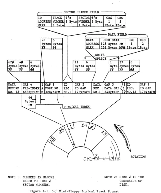
1.3.1.1 _togi'cal Track Format (5~" Mini Floppy)
The diskette surfaces are divided into 77 concentric cylinders numbered
0-76. Each cylinder consists of. two tracks. The track on side
0
containssectors 1-13 while the track on side 1 contains sectors 14-26. The track
begins and ends at the index address mark. The track is formatted in
such a way that this "softl l
index is preceded by the leading edge of the
physical index hole in the diskette. Following the physical index are
40 bytes of "FF" datc;l, 6 bytes of
"0"
data, a~d the index address markindicating the beginning of the track. Following the index address mark
is the post index gap consisting of 26 bytes of "FF" data and 6 bytes of
"0"
data. The next field is the sector header for the first sector. Onside 0 this is 1. On side 1 this sector is sector 14. Following the
sector header is the ID gap consisting of 11 bytes of tiFF" data and 6 bytes
of
!!0"
data. The next field is the data record for the sector. Followingthe data field is the data gap consisting of 28 bytes of "FF" data and
6 bytes of
"0"
data. This field reads to the next sector header. Followingthe 13th data record on side
0
and the 26th data record on side 1 is thepre-index gap consisting of approximately 620 bytes of "FF" data.
Each track is formatted in the above manner. Refer to Figure 1-1. The
sector header field of each sector contains information describing both
the sector and the track number. All the above fields are recorded in
FM
except as noted in the following sections.- - - SECTOR HEADER FIELD
SECTOR
0's
CRCByte NUMBER 1 Byte' 1
1 B te IB te
CRC
2
,...--- DATA FIELD - - - .
620
40
6Byt.es Bytes FF
11
DATA GAP 4 I GAP'· 1 ID GAP 2 RECORD PRE-INDEX A POST -NO. REe. ID GAP
NO. 13,
666B
tsFM M 32B NO.117B
tsFMNOTE 1: NUMBERS IN BLOCKS REFER TO SIDE
0
SECTOR NUMBERS.INDEX
USER DATA
128 Bytes FM 2 B
ROTATION
NOTE 2: SIDE
0
IS THEUNDERSIDE OF DISK.
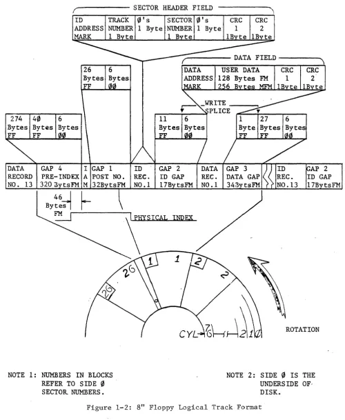
[image:10.613.44.563.71.695.2]1.3.1.2 Logical Track Format(8" Floppy)
The diskette surface is divided into 77 concentric tracks numbered 0-76.
Each track consists of 26 sectors numbered 1-26. A track begins and ends
at the index address mark. Each track is formatted in such a way that this
"soft" index is preceded by the leading edge of the physical index hole in
the diskette. Following the physical index are 40 bytes of "FF" data, 6
bytes of
"0"
data, and the index address mark indicating the beginning ofthe track. Following the index address mark is the post index gap
consisting of 26 bytes of "FF" data and 6 bytes of
"0"
data. The nextfield is the sector header for sector 1. Following the sector header is
the ID gap consisting of 11 bytes of "FF" data and 6 bytes of
"0"
data.The next field is the data record for sector 1. Following the data field
is the data gap consisting of 28 bytes of "FF" data and 6 bytes of
"0"
data. This field leads to the next secto header. Following the 26th
data record is the pre-index gap consisting of approximately 274 bytes of
"FF" data.
Each track is formatted in the above manner. Refer to Figure 1-2. The
sector header field of each sector contains information describing both
the sector and track number. All the above fields are recorded in FM
except as noted in the following sections.
r - - - -
SECTOR HEADER FIELDTRACK
0'5
SECTOR ~'s eRe eRC274 4~
DATA RECORD NO. 13
Bytes FF
GAP 4
PRE-INDEX
320:3 tsFM 26 Bytes FF
I GAP 1 A POST NO.
M 32B
~
NOTE 1: NUMBERS IN BLOCKS REFER TO SIDE ~ SECTOR NUMBERS.
1 Byte NUMBER 1 Byte' 1 2
ID
REC.
NO.1
1 B te
...,...---- DATA FIELD - - - .
GAP 2
ID GAP REC.
17B tsFM NO .1
ImlEX
USER DATA CRC CRC
128 FM 1 2'
2 6
ROTATION
NOTE 2: SIDE
0
IS THE UNDERSIDE OF-DISK. [image:12.617.63.563.87.696.2]1.3.2 Sector Header Field
The header field consists of 7 bytes of information. Preceding the
header is a field of bytes of "zero" data for synchronization. The
header and this preamble are always recorded 'in FM.
1. Byte 1. ID Address Mark - A unique mark consist~ng of 1 byte
of FE (hex) data with three missing clock-transitions using a
C7 (hex) clock pattern. This mark is decoded by the controller
and indicates the start of the sector header.
2. Byte 2. Track Address - This byte indicates the absolute
.(0-114
8) track address. Each sector contains this track
information to locate its position on one of the 77 tracks.
3. Byte 3. "Zero"
4. Byte 4. Sector Address - This byte indicates the absolute
(1-328) sector address. Each sector contains the information
to identify its position on the track.
5. Byte 5. "Zero"
6. Byte 6, 7. GRC - This is the 16 bit cyclic redundancy character
and is calculated for each header from the first 5 bytes of
information using the IBM 3740 polynomial. (Refer to Cyclic
Redundancy Check, Section 1.3.7)
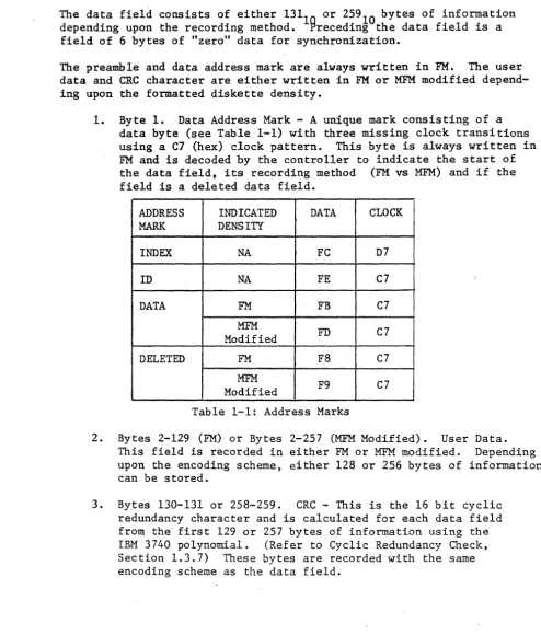
1.3.3 Data Field
The data field consists of either 131
1 or 25910 bytes of information
depending upon the recording method.
~receding
the data field is afield of 6 bytes of "zero" data for synchronization.
The preamble and data address mark are always written in FM. The user
data and CRC character are either written in FM or MFM modified
depend-ing upon the formatted diskette density.
1. Byte 1. Data Address Mark - A unique mark consisting of a
data byte (see Table 1-1) with three missing clock transitions using a C7 (hex) clock pattern. This byte is always written in
FM
and is decoded by the controller to indicate the start ofthe data field, its recording method (FM vs MFM) and if the
field is a deleted data field.
ADDRESS INDICATED DATA CLOCK
MARK DENSITY
INDEX NA FC D7
ID NA FE C7
DATA FM FB C7
MFM
FD C7
Modified
DELETED FM F8 C7
MFM
F9 C7
Modified
Table 1-1: Address Marks
2. Bytes 2-129 (FM) or Bytes 2-257 (MFM Modified). User Data.
This field is recorded in either FM or MFM modified. Depending
upon the encoding scheme, either 128 or 256 bytes of information can be stored.
3. Bytes 130-131 or 258-259. CRC - This is the 16 bit cyclic
redundancy character and is calculated for each data field from the" first 129 or 257 bytes of information using the
IBM 3740 polynomial. (Refer to Cyclic Redundancy Check,
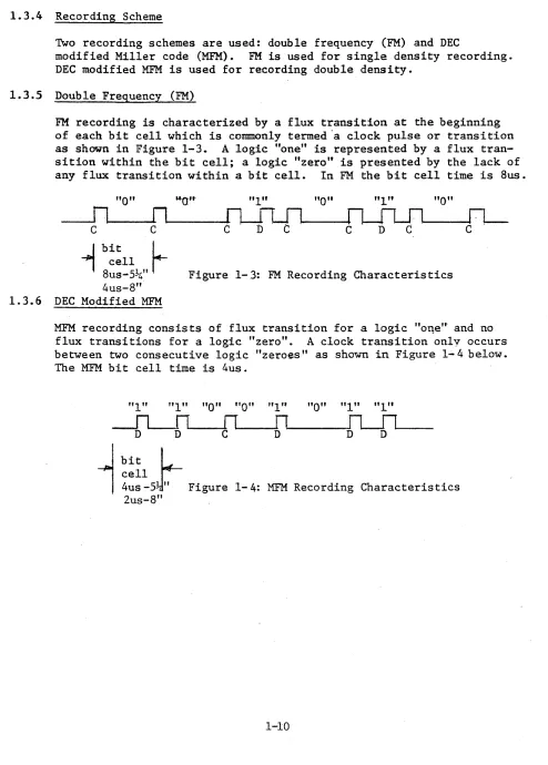
[image:14.620.61.556.136.717.2]1.3.4 Recording Scheme
Two recording schemes are used: double frequency (FM) and DEC
modified Miller code
(MFM).
FM
is used for single density recording.DEC modified
MFM
is used for recording double density.1.3.5 Double Frequency (FM)
FM
recording is characterized by a flux transition at the beginningof each bit cell which is commonly termed "a clock pulse or transition
as shown in Figure 1-3.
A
logic "one" is represented by a fluxtran-sition within the bit cell; a logic "zero" is presented by the lack of
any flux transition within a bit cell. In FM the bit cell time is 8us.
"0"
"1"
"0"
"1"
"0"
c
c
-1
bitL
8~::~~"
I
Figure 1-3: FM Recording Characteristics 4us-8"1.3.6 DEC Modified MFM
MFM recording consists of flux transition for a logic "OI\en- and no
flux transitions for a logic "zero".
A
clock transition onlv occursbetween two consecutive logic "zeroes" as shown in Figure 1-4 below.
The MFM bit cell time is 4us.
"1"
"1" "0" "0" "1"
"0" "1" "1"
bit cell
r.-4us -51" . Figure 2us-8"
~---~[l--fl----1-4: MFM Recording Characteristics
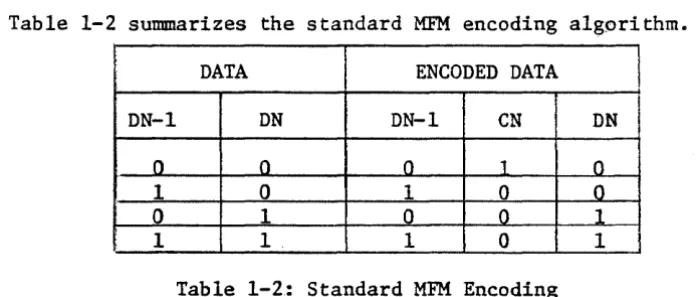
[image:15.612.63.557.102.792.2]Table 1-2 summarizes the standard MFM encoding algorithm.
DATA ENCODED DATA
DN-I DN DN-l eN DN
0 0 0 1 0
1 0 I 0 0
0 1 0 0 _1
1 1. 1 0 1
Table 1-2: Standard M~ Encoding
Because single density headers are used for both FM and MFM recording formats and since certain MFM patterns map into single density address marks, a modified algorithm is used. The mapping occurs when a data
pattern of exactly four consecutive "ones" is encoded. Whenever this
pattern is encoding a special algorithm is applied. Table 1-3 defines the encoding algorithm for this special case.
DATA
DN-5 DN-4 DN-3 DN-2 DN-l DN
0 1 1 1 I
a
x
0 1 0 0 0 1 0 0 0 I 0CN-5 DN-S CN-4 DN-4 CN-3 DN-3 CN-2 DN-2 CN-l DN-l CN DN
--- -
--ENCODED DATA
Table 1-3 : Modifying Algorithm (Special Case)
When reading double density data fields the controller checks for a missing clock bit between two zero data cells and if found, substitutes one's for the two zero data bits (generated by the special encoding algorithm).
1.3.7 Cyclic Redundancy Check
Each sector header field and data field has two byte eRC character
appended. This 16 bit character is the remainder that results when
dividing the data bits (represented as a polynomial M(x)) by a
genera£gr po12nomial G(x). The polynomial used for IBM 3740 is
G(x)=X + Xl + X5 + 1. For the sector header the data bits include
byte 1 thru 5. For an FM data' field the bits include byte 1 thru byte
[image:16.615.57.548.62.747.2] [image:16.615.108.456.111.259.2] [image:16.615.78.525.340.491.2]1.4 SPECIFICATION
RECORDING TECHNIQUE: 5~" Mini Floppy
Single Density Double Density 8" Floppy
Single Density Double Density
POWER REQUIREMENTS: Voltage
Current
ENVIORNMENTAL
Temperature Humidity
Modified IBM 3740 FM Modified DEC'MFM
IBM 3740 FM DEC Modified MFM
Single 5V supply
(from LSI-II backplane) 2.5A Typical
10% - 95% non-condensing
SECTION 2
INSTALLATION
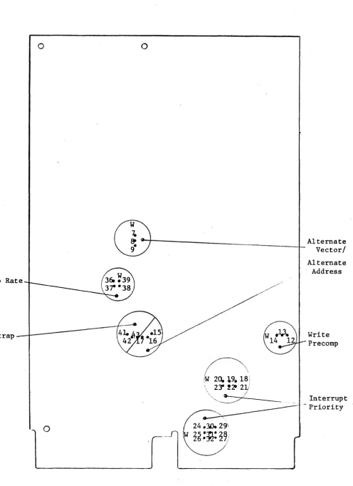
2.1 CONFIGURATION
The controller is shipped with standard options configured. The
device interrupt priority is set to level four. The firmware
bootstrap is disabled. Write precompensation is enabled.
Most options are factory foil-etched to the most often used
configuration. The foil jumpers must first be cut before the
alternate jumpers are inserted. Refer to Tables 2-1 and 2-2 for
alternate options and Figure 2-1 for jumper location. S~veral of
the options are selectable by using AMP 530153-2 pin jumpers. If
these pin jumpers are not available use # 30 wire wrap.
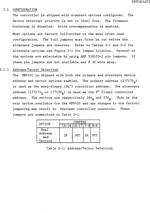
2.1.1 Address/Vector Selection
The MXV42C is shipped with both the primary and alternate device
address and vector options enabled. The primary address (1771708)
is used as the mini-floppy (5~") controller address. The alternate
address (1771748 or 1771508) is used as the 8" floppy controller
address. The vectors are respectively 264
8 and 2708. This is the
only option available for the MXV42C and any changes to the factory
jumpering may result in improper controller operation. These
jumpers are summarized in Table 2-1.
OPTION JUMPERS
15-16 16-17 7-8 8-9 Dual
Address
IN OUT IN OUT
and Vectors
[image:18.615.59.539.65.747.2]o
Step Rate
Bootstrap
o
CD;
r---____________________
LAlternate9
- Vector/
~\
iw
20.19_
18 \\ 23'!2t 2V
" I
"""'~//
Figure 2-1: Configuration Jumper Location
2-2
Alternate Address
Write Precomp
[image:19.615.63.560.54.737.2]·.JAri
•
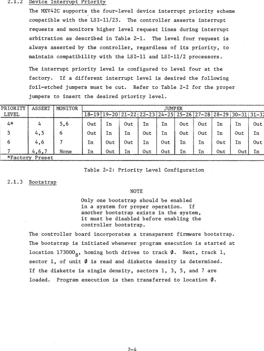
[image:20.617.86.521.56.719.2]2.1.2 Device Interrupt Priority
PRIORITY
The MXV42C supports the four-level device interrupt priority scheme
compatible with the LSI-ll/23. The controller asserts interrupt
requests and monitors higher level request lines during interrupt
arbitration as described in Table 2-1. The level four request is
always asserted by the controller, regardless of its priority, to
maintain compatibility with the LSI-II and LSI-ll/2 processors.
The interrupt priority level is configured to level four at the
factory. If a different interrupt level is desired the following
foil-etched jumpers must be cut. Refer to Table 2-2 for the proper
jumpers to insert the desired priority level.
ASSERT MONITOR JUMPER
LEVEL 18-19 19-20!2l-22 22-23 24-25 25-26 27-28 28-29 30-31131-32
4* 4 5,6 Out In
i
Out In In Out Out In5 4,5 6 Out In In Out In Out Out In
6 4,6 7 In Out Out In Out In In Out
7 4,6,7 None In Out In Out Out In In Out
*Factory Preset
2.1.3 Bootstrap
Table 2-2: Priority Level Configuration
NOTE
Only one bootstrap should be enabled
in a 'system for proper operation. If
another bootstrap exists in the system, it must be disabled before enabling the controller bootstrap.
The controller board incorporates a transparent firmware bootstrap.
The bootstrap is initiated whenever program execution is started at
location 1730008, homing both drives to track~. Next, track 1,
sector 1, of unit ~ is read and diskette density is determined.
If the diskette is single density, sectors 1, 3, 5, and 7 are
loaded. Program execution is then transferred to location ~.
2-4
In Out
Out In
In Out
[image:21.612.42.559.87.774.2]Controllers are shipped with this feature disabled. To enable the
bootstrap remove the jumper between W42 and W43 and insert the
jumper between W42 and W4l as shown in Table 2-3.
OPTION JUMPERS
41-42 42-43
B<?otstrap IN OUT
Enabled Bootstrap
OUT IN
Disabled* *Factory Set
Tabl~ 2-3: Bootst~ap Option
2.1.4 Write Precompensation
The MXV42C controller provides hardware write precompensation to
reduce the bit shift exhibited by all drives as the recorded flux
density increases. The controller recognizes the patterns which
produce bit shift and precompensates the written pattern. This
unique feature allows the controller to perform reliably with
any Shugart compatible drive.
Controllers are shipped with this feature enabled and it is
recommended that for more reliable operation the feature not be
disabled. However, if so desired, the feature can be defeated
by cutting the foil-etched jumper between W12 and W13 and inserting
a jumper between W13 and W14 as shown in Table 2-4.
OPTION JUMPERS
12-13 13-14
Write Precomp IN OUT
Enabled* Write Precomp
OUT IN
Disabled *Factory Set
[image:22.620.55.560.71.780.2]2.1.5 Step Rate Control
The MXV42C is shipped with a 3ms step rate for the mini-floppy (5~")
and 6ms step rate for the standard floppy 8". Alternate step rates
can be selected. Refer to Table 2-5 for option description and
jumper numbers.
OPTION JUMPERS
STEp·RATE 36-37 38-39
5~"
=
3ms*8"
=
6ms* IN IN5~"
=
6ms8" . = ·6ms OUT IN
5~"
=
3ms8"
=
3ms IN OUT5~"
=
6ms8"
=
3ms OUT OUT*Factory Set
Table 2-5: Step Rate
2.2 DRIVE CONFIGURATION
For proper operation the floppy drives must be configured with
attention to several options. The controller uses radial drive
selection. Thus the drive(s) should be correspondingly- configured.
2.2.1 Hfni-Floppy Configuration
The mini-floppy (5~") drives are configured as physical drive 3 and
drive 4. However, the drives are referenced by the pr:ima.ry controller
address register set and hence appear to the operating software as
unit
0
and unit 1 respectively. For details concerning these andother options refer to table 2-6.
DUAL SINGLE!
OPTION DESCRIPTION DRIVE 0 ! DRIVE 1 DRIVE OJ
DSl Drive select 0 Out Out Out
DS2 Drive select 1 Out Out Out
·DS3· . Drive select 2 In Out In
DS4 Drive select 3 Out In Out
HS In In In
lIM Out Out Out
MUX Out Out Out
Table 2-6: Hini-Floppy Drive Configuration
[image:23.613.56.563.57.741.2]2. 2. 2 8" ·Floppy Configuration
When two 8" drives are used, the first should be drive 1 and the
second drive 2. A particular drive is selected and remains selected
after a function is complete to allow the controller to poll drive
status. A seperate head load signal is provided by the controller
for read and write functions on the diskette. The "in use" logic of
the drive should be configured as a function of head loading. Since
the drives are homed without loading the heads during an initialize
command, the drive should be configured to provide stepper motor
power independent of head loading. For details 'concerning these and
other options refer to Table 2-7.
DUAL SINGLE
OPTION DESCRIPTION DRIVE 0 DRIVE 1 DRIVE 0
DSI Drive select 1 In Out In
DS2 Drive select 2 Out In Out
DS3 Drive select 3 Out Out Out
DS4 Drive select 4 Out Out Out
A Radial head loading option In In In
B Radial head loading option In In In
C Head load option In In In
D In use option Out Out Out
X Radial head loading option Out Out 'Out
WP Inhibit write when protect In In In
NP Allow write when protect Out Out Out
DS Stepper power from drive select In In In
HI.. Stepper from head load Out Out Out
Z In use from drive select Out Out Out
y In use from head load In In In
R* Ready output Out Out ; Out
I Index output In In In
DC Disk change output X X X
S Sector output X X X
800 Sector option Disable In In In
801 Sector option Enable Out Out Out
L -5V DC Bias In In In
Tl Termination HL Out In In
T2 Termination Drive Select In In In
T3 Termination Direction Out In In
T4 Termination Step Out In In
T5 Termination Write Data Out In In
T6 Termination Write Gate Out i In In
*If cable method B is used it is not necessary to remove this ,option
[image:24.613.67.533.290.678.2]2.3 CABLING
The 50 pin header located at the top edge of the controller board
provides all required interface signals for both the 8" and 5~"
Shugart compatible floppy disk drives. A 50 conductor ribbon cable
is used to connect the controller to any 8" Shugart compatible drive.
A 34 conduct ribbon cable, terminated to the upper 34 pins of the
50 pin socket connector, is used to terminate the controller to an~
5~" Shugart compatible drive. Two 8" and two 5~" drives are
simultaneously· connected to the controller using one of the two following
suggested methods.
Method A connects to all four drives using a single control cable
(See Figure 2-3). At one end of the 50 conductor ribbon cable a
50 pin socket connector is terminated and connects the 50 pin socket
connector to the controller card. At the required service length
of the cable two 50 pin card edge connectors are terminated and
connect to the 8" floppy disk drives. Beyond these connectors only
the upper 34 conductors are. r~quired. The unused conductor should be
trimmed. Again at the required service length two 34 pin card edge
connectors are terminated and connect to the 5~" mini-floppy drives.
Using this cabling method requires the removal of the'READY" (R)
option from both of the 8" floppy drives (Refer to Section 2.2).
NOTE
Only the last drive on the cable should be terminated. Remove the terminator
resistor arrays from the other drives. If more than two termination networks remain, loading of the interface signals will result in intermittent operation
and possible loss of data.
Ribbon Cab Ie (50 Conductor)
Pin 1
gTY
1 ea
2 ea
2 ea
AR
50
50
34
50
Pin 1
~~
Ribbon Cable (34 Conductor)i /
i_-t= ---
/
I
!
1 - - - l _ J - - - - L
J
Pin 1
____ ... Card Edge '\ '\ Card Edge
Connector Connector
(50 Pin) (34 Pin)
,;..~----Socket Connector (50 Pin)
DESCRIPTION MFG NUMBER
Pin Socket Connector 3M 3425-3000
Pin Edge Connector 3M 3415-0001
Pin Edge Connector 3M 3463-0001
Conductor Ribbon Cable 3M 3365/50
[image:26.613.89.578.50.550.2]Method B connects the mini-floppy drive(s) to the controller using
a cable configured with a 50 pin socket plug in place of the 50 pin
edge connectors discussed in method A. See Figure 2-4. This
socket plug will accept a standard 50 pin ribbqn cable assembly.
By removing pin 22 of this 50 pin plug connector the requirement to
remove the "READY" (R) option from the 8" floppy drive(s) is
eliminated. Standard configured 8" drives can thenLbe directly
plugged into this connector.
NOTE
Only the last drive on each cable assembly
should be terminated. Remove the terminator
resistor arrays from the other drives. If
more than two termination networks remain loading of the interface signals will result in intermittent operation and possible loss of data.
In both methods observe the alignment of pin 1 of the socket
connector and header as indicated by the arrows shown in Figure 2-3
and 2-4. The edge connectors should be connected to the corresponding
drives, again observing the location of pin 1.
The connector illustrated in Figure 2-5 is compatible with both the
Shugart compatible 8" and 5~" floppy drives. Any drive that has
both a Shugart compatible interface and connector should function
properly with the controller.
Ribbon Cable (50 Conductor)
Pin 1
~
Ribbon Cable (34 Conductor)/
jin
1
==~~~'-'-=-='-=--=--~'~~f ~'~'-~4
: i i i
_ I _ - - - ' : I
-L~
Plug Connector Card Edge
(50 Pin) Connector
*Pin 22 Removed (34 Pin)
Pin 1 ---~~--~,~
gTY
1 ea 50
1 ea 50
2 ea 34
A/R 50
~I--_ _ Socket Connector
/ /
DESCRIPTION
Pin Socket Connector
Pin Plug Connector
Pin Edge Connector
Conductor Ribbon Cable
(50 Pin)
MFG
3M
3M
3M
3M
NUMBER
3425-3000
3331-0001
3463-0001
3365/50
[image:28.612.100.577.46.591.2]2 4 6
8
101 1 2 r
-- Controller
Connector
TG 43
MOTOR ON
TWO SIDED
SIDE SELECT 8"
HEAD LOAD INDEX 8"
DRIVE SELECT 4
INDEX 5~rr DRIVE SELECT 1
DRIVE SELECT 2
DRIVE SELECT 3
MOTOR ON DIRECTION STEP
WRITE DATA WRITE GATE TRACK 00
WRITE PROTECT READ DATA
SIDE SELECT 5!-4"
==--:fi=1
~.
=--=fP
- - - 1 1 0~
----+112
---1i~"": 14
=~:~
:!--
--~ll
---j:it---26 ' '10 ;
- ~
---I!!!3D'-"""C~
·t~
. 32 i161
---~~~34; 1~
----~36: 20
----~38: 22
---~40: 24 - - - 4 2 : ,26
---~44~ 128
' - ,
--- 46 l i 30
- - - 48 : :i~;{32
---50, - - 1 ., 134
Drive Connector 8" Floppy
Drive Connector Mini-Floppy
Figure 2-5: Connector Pin Definition
[image:29.613.83.524.47.744.2]2.5 INITIAL OPERATION AND CHECKOUT
Before the following procedures are done, verify that the controller
has been configured as described in Sections 2.1-2.4.
NOTE
The bootstrap must be disabled for the following procedures.
1. Apply AC and DC power to the drive(s). The in-use indicators
on all drives should be off.
2. Place the Run/Halt switch on the processor to the Halt
position and turn on the processor. ,An "@" character
should be printed on the terminal signifying that console
ODT h~s been entered. All drives (first drive 1, then
drive
0)
of each set will step the heads inward 2-tracks,then step the heads outward until the home signal is detected.
The heads will not load, and if the drive is configured as
per Section 2.2, the in-use indicators will not light. If
the above events do not occur, check the cabling and drive
power supplies.
3. Open the CS register using ODT by typing 177170/ on the
terminal. The processor will display the contents of the
CS register. If the controller is operating properly a
004040
8 should be printed. Depo~it a 400008 in the CS
register by typing 40000 CR. This command will initialize
the controller. Both drives of each set should calibrate
for home position. First, drive 1 :steps outward 2 tracks
then inward one track at a time until the drive indicates
track
0
has been reached. The procedure is repeated ondrive
0.
The heads will not load and if the drive isconfigured as per Section 2.2, the in-use indicators will
4. Reopen the CS register (location 1771708) using ODT as
described above. The contents of this location should
be 00404°8" Examining the next location 177172/ should
yield a 04
8• For a detailed description of the register
protocol and bit definition, refer to Section 3.
5. If the above procedures function as described, the
controller is ready for use. Either diagnostics or an
operating system can be booted. For details on
boot-strapping refer to Section 4.2.
6. If the above procedures cannot be validated, consult the
factory of your local representative for assistance.
NOTE
For an LSI-1l/23 the CS and DB registers are addressed as 7771708 and 777172
8, respectively.
3.1 GENERAL
SECTION 3
FUNCTIONAL DESCRIPTION
This section describes device registers and command protocol for the MXV42C.
The MXV42C controls two 5~" mini-floppy drives and two 8" floppy drives.
All software control of the MXV42C is performed by means of two device
registers: the command and status (MXVCS) register and a multipurpose
data buffer (MXVDB) register. There is a set of registers to control each
type of drive. For the 5~" drives the MXVCS is assigned the address
1771708 and the MXVDB is assigned 177172
8. The MXVCS and MXVDB addresses
for the 8" drives are 1771748 and 177176
8 or(177l50 and l77l52},respectively.
The registers can be read or loaded, with a few exceptions, using any
instructions referring to their addresses.
The MXVCS register passes control information from the CPU to the
controller and reports status and error information from the controller
to the CPU. The MXVDB is provided for additional control and status
information between the CPU and the controller. The information that
is present in the MXVDB at any given time is a function of the controller
operation in progress.
NOTE
Loading one set of registers can affect
the contents of the other set. This
will not hinder operation of the con-trollers because once a command is initiated on a set of registers, only that set will act on data supplied to it.
The controller contains a sector buffer capable of storing a complete sector. For read/write operations the buffer is either "filled" before a write command or "emptied" after a read corrnnand under DMA control. During a write command the controller locates the desired sector and the buffer information is transferred
to the diskette. During a read operation
the desired sector is located and the
3.2 REGISTER DEFINITIONS
3.2.1 MXVCS - Command and Status Register (5!-4" - 1771708)(8" - 1771'748 or 1771508)
The format of the MXVeS register is shown below. Functions are initiated by loading the command and status (CS) register, when not busy (bit 5=1), with bit 0=1. Command protocol is discussed in detail in Section
3.3.
15 \.1 14 13 12 11
EX'1' ADDR RXO 2
6 5 INTR DONE
ENS
BIT DESCRIPTION
15 ERROR: This bit is set by the controller to indicate that an error has occurred during an attempt to execute a command. This bit is cleared by the initiation of a new command or by setting
the initialize bit. When an error is detected the MXVES is read into ~he MXVDB. This bit is a read-only bit.
14 MXV22M INITIALIZE: This bit is set by the program to ini tializE!
th~ controller without initializing all the devices on the LSI-II bus. This is a write-only bit.
12-13
(CAUTION)
Loading the lower byte of the MXVCS will also load the upper byte of the MXVCSo
When this bit is set, the controller will negate Done and move the head position mechanism of drive 1 (if two drives are available) to track O. When completed, the controller will repeat the operation on drive O.
The controller will then clear the error and status register, set Initialize Done, and set Drive Ready if drive 0 is ready. Finally, the controller will read sector 1, track 1, of drive O.
EXTENDED ADDRESS BITS: These bits are used to specify an extended bus address. Bit l2=MAl6. Bit l3=MAl7. These are write-only bits.
11 RX02: This bit is asserted by the controller to indicate that this is an RX02 type system. This is a read-only bit.
10 RESERVED: Must be ~"ritten as zeroes.
09 5~" NOT USED
8" HEAD SELECT: This bit selects one of the two possible sides of
the disk for execution of the desired function. When cleared,
side 0 is selected; when set, side 1 is selected. This is a
read/write bit.
08 DENSITY SELECT: This bit selects either single or double den~ity
operation. When cleared, single density is selected; when set,
double density is selected. This is a read/write bit.
07 TRANSFER REQUEST: This bit signifies that the controller needs
data or has data available. This is a read-only bit.
06 INTERRUPT ENABLE: This bit is set by the program to enable an
interrupt when the controller has completed an operation and
asserted the Done bit. The condition of this bit is cleared by
initialize. This is a read/write bit.
OS DONE: This bit indicates the completion of a function. Done ~ill
generate an interrupt when asserted if interrupt enable. (MXVCS bit 6) is set. This is a read-only bit.
04 UNIT SELECT: This bit selects one of the two possible disks for
execution of the desired function. This is a read/write bit.
03-01 FUNCTION SELECT: These bits code one of the eight possible
functions described in detail within this section. These are
write-only bits.
000 Fill Buffer
001 Empty Buffer
010 Write Sector
011 Read Sector
100 Set Media Density/Format
101 Read Status
110 Write Deleted Data Sector
III Read Error Code
00 GO: Initiates a command to the controller. This is a write-anly
bit.
3.2.2 MXVDB - Data Buffer (5~" - 1771728) (8" - 1771768 or 177152)
This register serves as a general purpose data path between the controller
and the LSI-II. It will represent one of six registers according to the
protocol of the function in process. These r~gisters include the 'KXVDB,
MXVTA, MXVSA, MXVWC, MXVBA, and MXVES.
This register is a read/write register if the controller is not in the
process of execut ing a cODDDand (i. e., it may be manipulated without
affec.ting the controller). When the controller is executing a command,
15
I
\15
Data Buffer Register (MXVDB)
All information transferred to and from.the floppy media passes through the MXVDB register and is' addressable only under the ,protocol of the function in progress.
14 .i.J J.2 11 10 9 9 7 6 5 4 3 2 1
MXVDB 'FORMAT
Track Address Reg.is ter (MXVTA)
o
This register is loaded to indicate on which of the 1158 (77 decimal) tracks a given function is to operate~ It can be addressed only under the protocol of the function in progress. Bits 8 through 15 are not used and are ignored.
MXVTA'FORMAT
Sector Address Register (MXVSA)
This register is loaded to indicate on which of the 328 (26 decimal) sectors a given function is to operate. It can be addressed only under the protocol of the function in progress. Bits 8 through 15 are not used and are ignoredc
14 13 12 11 10 9 9 7 6 5 4 3 2 1 o
MXVS,A.FDRMAT
15
Word Count Register (MXVWC)
This a-bit register is loaded with the number of words (maximum of 128 decimal) to be transferred. At the end of each transfer the word count register is decremented. When the contents of the
register are decremented to zero, transfers are terminated; Done is set (MXVES bit 5); and, if enabled, an interrupt is requested. If the word count is greater than the limit for the density specified, the controller asserts a Word Count Overflow (bit 10 of the MXVCS). This register can be addressed only under the protocol of the function in progress. Bits 8 through 15 are not used and are ignored.
14 13 12 11 10 9 a 7 6 5 4 3 2 1 o
~c FOR"fAT 0-200a
Bus Address Register (MXVBA)
This register is used to generate the bus address which specifies the location to and from which data are to be transferred. The register is incremented after each transfer. It will increment across 32K boundary lines via the extended address bits in the
control and status register. Systems with only l6_address bits will "wraparound" to location zero when the extended address bits are incremented. This register can be addressed only under the protocol of the function in progress, Bit 0 is not used and is ignored.
MXVBA FORMAT
Error and Status Register (MXVES)
15-12 Not Used
11 NONEXISTENT MEMORY ERROR: This bit is asserted by the controller
when the memory address specified for a DMA operation is nonexistent.
10 WORD COUNT OVERFLOW: This bit indicates that the word count
specified is greater then the limit for the density selected. Upon detecting this error the controller terminates the fill or empty buffer operation and asserts the Error and Done bits.
09 5~rr Not used
8" HEAD. SELECT: This bit indicates the side currently selected. If
cleared~ it indicates side
0;
of set, it indicates side 1.08 UNIT SELECT: This bit indicates the drive currently selected.
If cleared, it indicates drive
0;
if set, it indicates drive 1.07' DRIVE READY: This bit is asserted if the unit currently selected
exists, is properly supplied with power, has a diskette installed correctly, has its door closed, and has a diskette up to speed. This bit is only valid when retrieved via a read status function or at the completion of initialize when it indicates the status of
drive
0.
06 DELETED DATA: During data recovery, the identification mark
preceding tha data field was decoded as a deleted data mark.
05 DRIVE DENSITY:This bit indicates the density of the diskette in
the selected drive. When zero, it indicates single density: when set to one, it indicates double density.
04 DENSITY ERROR: A density error was detected as the information
was retrieved from the data field of the diskette (a density error occurs when the density selected differs from that of the
data field). Upon detecting this error the controller loads the
MXVES into the MXVDB and asserts the Error and Done bits.
03 ACLO - This bit is set by the controller to indicate a power
failure.
02 INITIALIZE DONE: This bit is asserted to indicate completion of
the initialize routine which can be caused by system power failure or programmable LSI-II bus initialize.
01 5~" Not Used
8" SIDE READY: This bit is asserted by the controller when a double sided drive is selected, is ready, and has double-sided media inserted. The. assertion of this bit indicates that side 1 of the selected drive is available for read and write operations.
00 CRC ERROR: A cyclic redundancy check error was detected as
information was retrieved from a data field of the diskette. The information stored in the buffer should be considered invalid. Upon detection of this error the controller loads the MXVES into
the MXVDB and asserts the Error and Done bits.
3.2.3 Extended Status Registers
The controller has four internal status registers. These registers provide specific error information in the form of error codes as well as drive status information depending upon the general error type.'
The registers can be retrieved by a read error code function as des~
cribed in Section 3.3. 8~
Word 1 <7:0> -Definitive Error Code
Octal Code Error Code Meaning
040 Tried to access a track greater,than 76.
050 Home was found before desired track was reached.
070 Desired sector could not be found after looking at 52·
headers (2 revolutions).
120 A preamble could not be found.
150 The header track address of a good header does not
compare with the desired track.
160 Too many tries for an IDAM (identifies header).
170 Data AM not found in allotted time.
200 CRe error on reading the sector from the disk.
240 Densi ty Error.
250 Wrong Key' word for Set Media Density Command .
260 Illegal Data AM.
270 Invalid pQK during write sequence.
300 Drive not ready.
310 .Drive write protected.
Word 1 <15:8> -Not Used
This register is always cleared by the controller.
Word 2<7 :0> -Current Track Address of Drive 0
Word 2 <J5:8;>-Current Track Address of Drive 1
This register is cleared during the initialize command in order to synchronize with actual track position. The register is updated with each seek on drive 1 and maintains current track position.
Word 3 <]:0;> Target Track of Current Disk Access
If .legal~ the track specified for· the last read/write command is
saved in this register.
Word 3 <J5:S:> Target Sector of Current Disk Access
The sector specified for the last read/write command is saved in this regis ter.
Word 4 <15:8> Track Address of Selected Drive'
This register contains the track address read from the sector header of the desired sector during the last read/write command.
3.3 COMMAND PROTOCOL
Data storage and recovery using theMXV2ZM controller is accomplished by careful manipulation of the MXVCS and MXVnB registers according to
the strict protocol of the individual functions. The penalty for violation of protocol can be pennanent loss' of data. Each of the
func-tions are encoded and written into the command and status register bits 1-3 as described in Section 3.2.1. The detailed protocol for each function is described below.
3.3.1 Fill Buffer (000)
This function is used to fill the controller buffer with data from the host processor. The number of words to transfer is specified by the host. The command density bit determines the buffer size (64 or 128 words). The controller zero-fills the remaining buffer space. If the word count is too large for the density selected the function is aborted,
Error and Done are asserted and the Word Count Overflow bit is set in the HXVES.
The contents of the buffer may be written on the diskette with a sub-sequent write sector command or returned to the host processor using an empty buffer command.
When the command is loaded, MXVCS bit 5 (Done) is negated. MXVCS bit 8 (density) must be set to define the buffer size. MXVCS bits 12 and 13 (extended address bits) must also be asserted to define the extended memory segment used with the buffer address, yet to be specified, to form the absolute memory address of the data to be transferred. MXVCS bit 4 (unit select) is ignored since no drive operation is required. When MXVCS bit 7 (TR) is first asserted, the program must move the word .count into the MXVDB which will negate TR.
When the controller again asserts TR, the program must move the buffer
address into the MXVDB. The controller then negates TR, initiates a
DMA cycle, and transfers the first word. from··the host processor to the controller buffer. At the end of the transfer the word count register
is decremented and the buffer address is incremented by two. This
cycle is repeated until the word count register becomes zero. The controller zero-fills the remaining buffer space, sets the Done bit, and if enabled, causes an interrupt request. After Done is asserted the MXVES is moved into the MXVDB.
During the Data rransaction, if any non-existent memory is addressed,
the controller will time out and abort the function. The Error and
Done bits will be asserted. MXVES bit 11 (NXM) will be set and the MXVES will be moved into the MXVDB; if enabled, an interrupt request will be generated.
3.3.2 Empty Buffer (001)
This function is used to transfer the contents of the controller to the
host processor. The number of words to transfer is specified by the
host. The command density bit determines the maximum legal word count. If the word count specified is too large for the density selected the function is aborted, Error and Done are asserted and the Word Count Overflow bit is set in the MXVES.
The contents of the buffer may be transferred to the host as many times as desired or may be written on the diskette with a subsequent write
sector command. Unless a fill buffer or read sector command is issued,
When the command is loaded, MXVCS bit (Done) is negated, MXVCS bit 8 (density) must be set to allow the proper word count limit. MXVCS.bits 12 and 13 (extended address bits) must also be asserted to define the extended memory segment used with the buffer address, yet to be speci-fied, to form the absolute memory destination address. MXVCS bit 4 (unit select) is ignored since no drive operation is required. When
HIVeS bit 7 (TR) is first asserted the program must move the word count
into the MXVDB which will negate TR. When the controll~r again asserts
TR the program must move the buffer address into the MXVDB. The
con-troller then negates TR, initiates a DMA, and transfers the first word of the buffer to the host processor. At the end of the transfer, the word count register is decremented and the buffer address register is incremented by two. This cycle is repeated until the word count reg-ister becomes zero. The controller then sets the Done bit and if en-abled,causes an interrupt request. After Done is asserted the MXVES is moved into the MXVDB.
During the DMA transaction, if ·any non-existent memory is addressed,
the controller will time out and abort the function. The Error and
Done bits will be asserted. MX.VES bit 11 (NXM) will be set and the
MXVES will be moved into the MXVDB. If enabled, an interrupt request
will be generated.
3e3e3 Write Sector (010)
This function is used to locate a desired track. and sector and write the sector with the contents of the internal sector buffer. When the MXVCS is loaded with this command, the MXVES is cleared and both the TR and Done bits are negated. tihen TR is first asserted the program must load the desired sector address into the MXVDB which will negate
TR. WhenTR is again asserted the program must load the desired track
address into the MXVDB which will negate TR. The controller then seeks
the desired track and attempts to locate the desired sector. The
desired track is compared with the track field of the sector field. If they do not match the operation is aborted, the Error and Done bits are asserted, the MXVES is moved into the MXDB, and if enabled the controller will assert an interrupt.
If the densities agree but the controller is unable to locate the desired sector within two diskette re7olutions, the controller will abort the operation, move the contents of MXVES into MXVDB, assert the Error and Done bits, and if enabled, assert· an interrupt request.
If the desired track and sector are located and the densities agree, the controller will write the contents of the internal sector buffer
followed by a CRe character, all in the function: selected density. The
controller completes the operation by moving the MXVES to the MXVDB,
asserts Done, and if enabled, asserts an interrupt request.
(CAUTIOil)
The contents of the internar sector buffer are lost during a power failure. However, after power is brought back to normal, a write sector command will cause the random contents of the buffer to be written on the diskette with a
valid
CRe
character.( NOTE)
The contents of the sector buffer are not destroyed by a write sector operation.
3.3.4 Read Sector (011)
This function is used to locate the desired track and sector and transfer the contents of the data field into the controller's internal sector buffer. When the MXVCS is loaded with this command, the MXVES is
cleared and both the TR and Done bits are negated. When TR is first
asserted the program must load the desired sector address 'into the
MXVDB which will negate TR. When TR is again asserted the program must load the desired track address into the MXVDB which will negate
TR.
Both the TR and Done bits remain negated while the controller attempts
to locate the desired sector. If after two revolutions the controller
is unable to locate the desired sector" the operation is aborted. The controller will move the MXVES into the-MXVDB, assert the Error and Done bits, and if enabled, assert an interrupt request.
When the desired sector is located, the controller will then compare.
the desired track with the track field of the sector header. If they
do not match, the operation is aborted. The Error and Done bits are
asserted, the MXVES is moved into the MXVDB, and if enabled, the
con-troller will assert an interrupt request. NOTE
Since there is only enough memory to store one sector of data internal to the MXV42C controller,
reading a sector u~ing first one set of drives than
the other will destroy the data from the first set. This does not present a problem since a read sector is normally followed by an empty buffer.
Note that user written drivers can transfer data
between the 5!z;" "and 8" diskettes without performing
3.3.5 Set Media Density (100)
This function is dual purpose. The controller can set the media density
by rewriting all the data address marks (single of double density) and
writing zero data fields in the selected density. The controller can
also "reformat" the entire diskette by rewriting both the sector headers
and the data fields. The data fields are written in the selected density
preceded by the corresponding data address mark. Both commands are
initiated by the set media function but differ in the keyword required by the controller to execute the command.
When the MXVCS is loaded with the command, the MXVES is cleared and the
Done bit is negated. When TR is set, the program must respond with a
keyword. This keyword must be deposited in the MXVDB to complete the
protocol. When the controller recognizes this character, it begins
executing the command. If an illegal keyword is used, the operation is
aported. The MXVES is moved into the MXVDB, the Error and Done bits are
set, and if enabled, the controller asserts an interrupt request.
If the keyword used is a 1118, the controller initiates a set media
density operation. This operation starts at track 0, sector 1. Each
sector header is located and a write operation is initiated. A data
field is written with zero data in the density selected. If an error
occurs reading any header, the operation is aborted. The MXVES is
moved into the MXVDB, The Error and Done bits are set, and if enabled,
the controller asserts an interrupt request. If the operation is
successfully completed, Done is set and if enabled, the controller asserts an interrupt request.
If the keyword used is a ,2228, the controller initiates a format operation.
This function starts at the physical index of track
0.
Each track iswritten first with an index address mark, then 26 sector headers are
written as described in Section 403. When each track (or cylinder)
has been written, the controller initiates a set media density function as described above.
CAUTION
The set media density function takes about 30 seconds and the format function takes
about 90 seconds for the 5!z;" mini-floppy. For the 8" floppy, the times are approx-imately 25 seconds and 50 seconds, respec-tively. Neither operation should be interrupted. If an error occurs or
either operation is ,interrupted, an illegal diskette may have been generated and the operation should be'repeated.
3.3.6 Read Status (101)
This function is used to update the drive status information and
is initiated by loading the command into the MXVCS. The Done bit
is negated. MXVES bit 7 (Drive Ready) is updated by sampling the
drive ready status line. Drive density is updated by loading the head of the selected drive and reading the first data address
mark. The controller then moves the MXVES into the MXVDB,
asserts Done, and if enabled, asserts an interrupt request. This
operation requires about 250ms to complete.
3.3.7 Write Deleted Data Sector (110)
This operation is identical to Write Sector (010) with one except ion. The data address mark preceding the data is not the
standard data address mark. A single or double density 'deleted
data address mark is written according to the density of the function.
3.3.8 Read Error Code (111)
This function is used to retrieve the extended status registers
and is initiated by loading the MXVCS with the command. The Done
bit is neg~ted. When TR is asserted, the program must load the
Bus Address into the MXVDB which negates TR. The controller
assembles one word at a time a