Themed Section: Science and Technology
Design and Hardware Implementation of a Nine level Inverter
with Less Switches Operating in Stand-Alone Mode
Vinay Potdar1, Shankar Vanamane2
1P. G. Student, Walchand College of Engineering, Sangli, Maharashtra, India 2Assistant Professor, Walchand College of Engineering, Sangli, Maharashtra, India
ABTRACT
This paper presentss a single-phase nine-level (9L) inverter configuration which can be suitable for grid-connected renewable energy systems. The proposed inverter is realized using a T-type neutral point-clamped inverter connected in series to a flying capacitor (FC) H-bridge. A self-voltage balancing based on superfluous switching state is developed and integrated with PWM controller, which is responsible for constrain the FC voltage at one-fourth of the input dc source voltage. The advance PWM technique employs the generation of 9L waveform without using any voltage sensor, thereby reducing the complicacy of the overall control scheme. In comparison to conventional and recent configurations, generation of the 9L waveform using a lower number of components is the notable contribution. Furthermore, a compendious comparison study is included which confirms the merits of the proposed inverter against those of other state-of-the art topologies. Finally, simulation results are included for validating the feasibility of the proposed system.
Keywords: Flying Capacitor, Nine-Level Inverter, Power Quality, Sensorless Voltage Control.
I.
INTRODUCTIONIn recent days price of petroleum oil is increased and the environmental conditions are also becoming worst so that demand of electrical energy is increased. To supply this demand for electrical energy has elevated the need for generating energy from alternate sources. A simple three-level (3L) inverter presented by Nabae et al. [1] is one of the standard topology that has gained more attention. However, there are also some disadvantages like high switching frequency, high acoustic noise and for voltage levels greater than three level more number of dc sources are used due to that more power loss occurs [2].The concept of multilevel inverters (MLI) has been introduced since mid-1970. The term multilevel originated with the three-level inverter. Subsequently, several multilevel inverter topologies continue to emerge, especially in the last two decades. Multi-Level inverters are power
conversion systems designed by power semiconductors and DC voltage sources that, when appropriately connected and controlled. They can generate a multiple-level-step voltage waveform with variable and controllable frequency, phase and amplitude [3].
from renewable energy sources like photovoltaic systems [6-9]. Several innovative inverter topologies with a claim of a reduced part count (RPC) are reported in literature [10], [11].
The topology proposed in [12] can generate a Seven Level output voltage waveform with RPC. However it has disadvantage of unbalancing in capacitor voltage and control technique become more complex. An analyzed survey of applicable nine level inverters for distributed generation (DG) system is presented in [13]. Also, a new topology with a cascade connection of 5L active neutral-point-clamped (ANPC) and 3L floating capacitor (FC) H-bridge is proposed. A combination of CHB with FC H-bridge presented in [14] consists of one dc source and eight switches only. However, regulation of FC voltage at 1/3Vdc requires
additional circuit. A configuration which includes 5L double flying capacitor multicell (DFCM) converters cascaded with FC Hbridge is recommended in [15] to overcome the increased diversity factor in a DFCM converter. A nine level cross-connected intermediate level unit integrated with ANPC is introduced in [16]. Most of these topologies are hybrid combinations of one or more converter families (NPC, FC, and CHB). Many such hybridizations resulting in nine level RPC inverter these are reported in literature [17]–[19]. Although for same voltage levels, the topologies mentioned require a lesser number of components, higher complexity in control mechanism.
This paper presents the Nine-level inverter for single phase system using self-voltage balancing technique integrated PWM technique. The paper is organized as follows. Section II explains nine level inverter. Section III explains the comparative study of the inverter. Section IV explains experimental results with harmonic analysis and Section V summarizes the result.
II.
PROPOSED NINE-LEVEL INVERTER CIRCUIT DESCRIPTIONA. Circuit Description
Fig. 1 shows the power circuit topology of the proposed nine level inverter. It consists mainly three units; a 3L TNPC cascaded with 3L FC H-bridge unit and two low-frequency switches (LFS) across the dc-link. With Vdc is the total input voltage, the voltages
across the dc-link capacitors and FC are equal to Vdc/2
and Vdc/4 respectively. The idea of seriesing of TNPC
with FC yields in the following advantage of less number of power switches, power diodes, and capacitors. Ideally, the inverter is capable of generating nine levels of output voltage: ±Vdc, ±3Vdc/4,
±Vdc/2, ±Vdc/4, 0. At a first sight, the series
configuration of TNPC and FC with two LFS might seem unnoticeable. In the absence of a LFS unit, with the dc-link midpoint being the return path for the output current, the cascade combination of TNPC and FC can only generate five levels: ±Vdc/2, ±Vdc/4, 0. As a
result, it can combines output voltage with additional levels: ±Vdc and ±3Vdc/4. For this, power switches are
to be gated appropriately in a sequence. Table I summarizes all the possible switching combinations and their effect on the FC voltage. Assuming the devices to be ideal, FC is large enough and load as pure resistive, the active current path over a positive half cycle of the output voltage for each level is obtained as follows:
1) Maximum positive output (Vdc): This voltage is
designated as S4+. Switches S1, S3, and S4 are ON,
connecting the terminal a to Vdc, and S5- is ON,
connecting the terminal b to ground.
2) Three-fourth positive output (3Vdc/4): Two
switching configurations are available. For S31+,
switches S1-, S2-, S3-, and S4 are ON, connecting the
terminal a to Vdc/4, and S5- is ON, connecting the
terminal b to ground. Thus the voltage across the load is V0 = Vdc/2 + Vdc/4 = 3Vdc/4. For S32+,
terminal a to −Vdc/4, and S5- is ON, connecting the
terminal b to ground.
Fig. 1. Circuit topology of the inverter.
3) Half-level positive output (Vdc/2): This voltage is
designated as S2+. Switches S1-, S2-, S3 and S4 are ON,
connecting the terminal a to Vdc/2, and S5- is ON,
connecting the terminal b to ground. Thus the voltage across the load is V0 = Vdc/2 + 0 = Vdc/2. 4) One-fourth positive output (Vdc/4): Two switching
combinations are available. For S11+, switches S2,
S3- and S4 are ON, connecting the terminal a to
Vdc/4, and S5- is ON, connecting the terminal b to
ground. For S12+, switches S1, S2-, S3, and S4- are ON,
connecting the terminal a to +Vdc/4, and S5- is ON,
connecting the terminal b to ground. Thus the voltage across the load is V0 = Vdc/2 − Vdc/4 = Vdc/4. 5) Zero output: Two switching combinations are
available. For S0+, switches S2, S3 and S4 are ON,
connecting the terminal a to ground, and S5- is ON,
connecting the terminal b to ground. For S0-,
switches S1, S3 and S4 are ON, connecting the
terminal a to Vdc, and S5 is ON, connecting the
terminal b to Vdc. In both cases, the terminal ab is
short circuited, and the voltage across the load is zero.
Consequently, the number of active power switches in the circuit current path is lower in comparison to and hence, this topology has a better efficiency.
B. Sensorless voltage balancing controlling integrated into PWM Technique
Nine-level PWM scheme including four carriers’ waves and the sinusoidal reference waveform is depicted in Fig. 2. The four carriers’ waveforms (Cr1,
Cr2, Cr3, and Cr4) are shifted vertically to modulate the
reference waveform (Vref) completely [20, 21]. The
firing pulses associated with switching states 1, 2, 3, 4 and 5 (as listed in table I) are generated based on comparing Vref with those carrier waves. Moreover,
surplus switching states of 4 and 5 are used to minimize the switching frequency. If Vref is positive,
then state 4 will be used to produce the zero level at the output. On the other hand, if Vref is negative, the
output zero level voltage will be generated by state 5. The described algorithm is shown in Fig. 2 which can produce the nine-level voltage waveform at the output without any feedback sensor.
TABLE I
SWITCHING STATES AND THEIR IMPACT ON FC VOLTAGE OF THE PROPOSED INVERTER
Stat es
Q
1
Q
2
Q
3
Q
4
Q
5
Outpu t voltage
FC voltage
S4+ 1 0 1 1 0 Vdc No effect S31+ 0 0 0 1 0 3Vdc/4 Dischargin
g
S32+ 1 0 1 0 0 3Vdc/4 Charging
S2+ 0 0 1 1 0 Vdc/2 No effect
S11+ 0 1 0 1 0 Vdc/4 Disharging
S12+ 0 0 1 0 0 Vdc/4 Charging
S0+ 0 1 1 1 0 0 No effect S0− 1 0 1 1 1 0 No effect S11− 1 0 1 0 1 −Vdc/4 Dischargin
g
S12− 0 0 0 1 1 −Vdc/4 Charging
S2− 0 0 1 1 1 −Vdc/2 No effect
S31− 0 0 1 0 1 −3Vdc/
4
S32− 0 1 0 1 1 −3Vdc/
4
Charging
S4− 0 1 1 1 1 −Vdc No effect
Fig.2 open-loop switching algorithm for self-voltage balancing of inverter
As mentioned before, applying the proposed algorithm on above inverter generates Nine-level voltage waveform at the output without using any voltage sensors and complex calculations in controller. The capacitor voltage would be constant even at start-up and also in load change conditions.
III.
COMPARATIVE STUDY OF MULTILEVEL
INVERTERTable II shows the components count in popular multilevel inverters as well as the presented inverter in case of producing single-phase 9-level output voltage waveform. It is prominent that the presented inverter with the sensor-less voltage balancing technique has the less components as well as its control scheme complexity is very low.
TABLE II
COMPONENTS COUNT FOR SINGLE-PHASE NINE-LEVEL INVERTERS
Invert er type
DC Sour ce
Cap acit or
Cla mpe d Dio de
Acti ve Swit ch
Total Part Count
Cont rol Com plexi ty
CHB 4 0 0 16 20 Low
NPC 8 0 14 16 38 Very
high
FC 1 7 0 16 24 High
Prese nted Invert er
2 3 0 10 15 Very
Low
As a comparison between conventional inverter and the proposed nine level inverter, it should be noted that the other inverters needs a very complicated controller to produce desired voltage levels at the output which requires adjusting a lot of controller gains in practical works[24-26]. Moreover, the controller design needs a lot of effort in modelling the system accurately and using many state variable feedbacks that increase the number of state variables and consequently voltage and current sensors. Mainly, It is highly dependent on the system parameters including load, connection line resistance and inductance, switching frequency, sampling time, DC source voltage amplitude, DC capacitor value, modulation index and output voltage frequency. Less complex controller and lower switching frequency are some advantages of the proposed nine level inverter with less number of components.
IV.
EXPERIMENTAL RESULTS
MATLAB simulation of nine level inverter is simulated to check the results. The voltage balancing of capacitor is validated in both stand-alone mode and grid connected modes. The parameters are Grid voltage-240V,50 Hz, Grid link inductor-1.5mH, DC Source Voltage-240V,Switching Frequency-2.5kHz, Stand Alone RL load-10 Ohm,30mH, Dc floating Capacitor-2.5uF
A. Stand Alone Mode
and DC supply. Here, the inverter supplies an RL type of Load.
Fig. 4(a) shows the starting of inverter. The capacitor is charged up to the one-fourth of the DC source. This happen because of self-voltage balancing technique and Sinusoidal PWM technique, so that nine level symmetric output voltage is generated. From result we can that Capacitor is need not to be charged previously, because of this switching technique. The Fast Fourier Transform (FFT) analysis of inverter output current is carried out and it is shown in fig.5 (c). It should be mentioned here that the THD of the output current is less than 10% and it is achieved without using any kind of harmonic filters
(a)
(b)
(c)
(d)
Fig. 4. Simulation results: (a) Inverter’s Nine level output voltage. (b)Output current of RL load (c) THD of the load current from FFT analysis. (d) Voltage across dc-link capacitors for a step change in dc source amplitude
.
Fig 4 (d) shows that, when the dc source voltage is changed and capacitor voltage is tracking the reference value exactly. This shows that the sensorless voltage regulator technique is integrated into the proposed PWM technique.
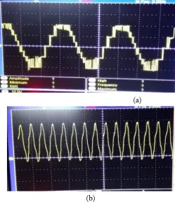
B. Hardware Implementation
The following fig. 5 shows the hardware setup of the proposed inverter. 10 separate power supply given to the 10 gate driver circuits. Dual power supply is used to give two battery supply for the inverter. In this experiment gate pulses for the inverter are given by Arduino MEGA 2560 microcontroller. Digital Oscilloscope is used to check the output waveform of the inverter.
(a)
(b)
Fig. 6. Hardware results: (a) Inverter’s Nine level output voltage of RL load (b) Voltage across dc-link capacitors for a step change in dc source amplitude
Thus we got the nine level of the output voltage. The distortion of the capacitor voltage is also shown. The waveform is not smooth. Due to the improper capacitance values and also the loose connections. This whole setup is run by using ARDUINO (Mega2560) micro controller on the low switching frequency, so that the proper nine level output voltage waveform is not getting. There is also the voltage imbalance between the voltage levels of the capacitor which are connected at the input side. To avoid this imbalance, capacitors of proper value will be used in next setup. There is also the power losses in the wiring of the inverter.
V.
CONCLUSION
Multilevel inverters are being developed and extensively exploited for generating high quality output voltages for numerous medium-voltage application fields. Applications urging a higher number of voltage levels escalate the number of
components required. But use of high number of part counts in conventional multilevel inverters increases both the circuit intricacies as well as the control scheme involved, thereby resulting in higher cost implications and reduced reliability. Therefore, to subdue these disadvantages, this proposes a novel hybrid 9L inverter topology formed by cascading a TNPC and FC with two LFS connected across the dclink. This is achieved using only ten power switches (among which two are operated at line frequency). Only one FC is incorporated in the circuit for generating the 9L output voltage. Further, it is confirmed that the proposed inverter structure has improved reliability and by cascading additional FCs, it can be effortlessly extended to obtain even higher number of voltage levels. In addition, a sensorless PWM technique based on the principle of energy balance for regulating the voltage of FC is suggested. An exhaustive review of recently proposed multilevel inverter topologies with RPC applicable for grid integration of renewable sources is carried out and the ensuing comparison certifies the merits of the proposed topology over conventional inverters.
VI.
REFERENCES[1] A. Nabae, I. Takahashi, and H. Akagi, “A new neutral-point-clamped pwm inverter,” IEEE Trans. Ind. Appl., vol. IA-17, no. 5, pp. 518–523, Sept 1981.
[2] V. Agelidis, D. Baker, W. Lawrance, and C. Nayar, “A multilevel pwm inverter topology for photovoltaic applications,” in Industrial Electronics, 1997. ISIE’97., Proceedings of the IEEE International Symposium on, vol. 2. IEEE, 1997, pp. 589–594.
[4] L. G. Franquelo, J. Rodriguez, J. I. Leon, S. Kouro, R. Portillo et al., “The age of multilevel converters arrives,” IEEE Ind. Electron. Mag, vol. 2, no. 2, pp. 28–39, 2008.
[5] S. Kouro, M. Malinowski, K. Gopakumar, J. Pou, L. G. Franquelo, B. Wu, J. Rodriguez, M. A. Perez, and J. I. Leon, “Recent advances´ and industrial applications of multilevel converters,” IEEE Trans. Ind. Electron., vol. 57, no. 8, pp. 2553–2580, 2010.
[6] C. Cecati, F. Ciancetta, and P. Siano, "A multilevel inverter for photovoltaic systems with fuzzy logic control," IEEE Trans. Ind. Electron., vol. 57, no. 12, pp. 4115-4125, 2010. [7] M. Seyedmahmoudian, S. Mekhilef, R. Rahmani,
R. Yusof, and E. T. Renani, "Analytical modeling of partially shaded photovoltaic systems," Energies, vol. 6, no. 1, pp. 128-144, 2013. [8] H. Mortazavi, H. Mehrjerdi, M. Saad, S.
Lefebvre, D.Asber, and L. Lenoir, "A Monitoring Technique for Reversed Power Flow Detection With High PV Penetration Level," IEEE Trans. Smart Grid, vol. 6, no. 5, pp. 2221-2232, 2015. [9] V. Biagini, P. Zanchetta, M. Odavic, M. Sumner,
and M. Degano, "Control and modulation of a multilevel active filtering solution for variable-speed constant-frequency more-electric aircraft grids," IEEE Trans. Ind. Informat., vol. 9, no. 2, pp. 600-608, 2013.
[10] K. K. Gupta, A. Ranjan, P. Bhatnagar, L. K. Sahu, and S. Jain, “Multilevel inverter topologies with reduced device count: a review,” IEEE Trans. Power Electron., vol. 31, no. 1, pp. 135–151, 2016.
[11] Y.-H. Liao and C.-M. Lai, “Newly-constructed simplified single-phase multistring multilevel inverter topology for distributed energy resources,” IEEE Trans. Power Electron., vol. 26, no. 9, pp. 2386–2392, 2011.
[12] N. A. Rahim, K. Chaniago, and J. Selvaraj, “Single-phase sevenlevel grid-connected inverter for photovoltaic system,” IEEE Trans. Ind. Electron., vol. 58, no. 6, pp. 2435–2443, 2011.
[13] J. Li, S. Bhattacharya, and A. Q. Huang, “A new nine-level active npc (ANPC) converter for grid connection of large wind turbines for distributed generation,” IEEE Trans. Power Electron., vol. 26, no. 3, pp. 961–972, 2011. [14] G. Buticchi, D. Barater, E. Lorenzani, C.
Concari, and G. Franceschini, “A nine-level grid-connected converter topology for single-phase transformerless pv systems,” IEEE Trans. Ind. Electron., vol. 61, no. 8, pp. 3951–3960, 2014.
[15] V. Dargahi, A. K. Sadigh, G. K. Venayagamoorthy, and K. Corzine, “Hybrid double flying capacitor multicell converter and its application in grid-tied renewable energy resources,” IET Gener. Transm. Distrib, vol. 9, no. 10, pp. 947–956, 2015.
[16] T. Chaudhuri, P. Barbosa, P. Steimer, and A. Rufer, “Cross-connected intermediate level (CCIL) voltage source inverter,” in 2007 IEEE Power Electronics Specialists Conference, June 2007, pp. 490–496.
[17] M. D. Manjrekar, P. K. Steimer, and T. A. Lipo, “Hybrid multilevel power conversion system: a competitive solution for high-power applications,” IEEE Trans. Ind. Appl., vol. 36, no. 3, pp. 834–841, 2000.
[18] M. Veenstra and A. Rufer, “Control of a hybrid asymmetric multilevel inverter for competitive medium-voltage industrial drives,” IEEE Trans. Ind. Appl., vol. 41, no. 2, pp. 655–664, March 2005.
Trans. Power Electron., vol. 60, no. 9, pp. 3627– 3636, 2013
[20] M. Sharifzadeh, H. Vahedi, A. Sheikholeslami, P.-A. Labbé, and K. Al-Haddad, "Hybrid SHM-SHE Modulation Technique for Four-LegNPC Inverter with DC Capacitors Self-Voltage-Balancing," IEEE Trans. Ind. Electron., vol. 62, no. 8, pp. 4890-4899, 2015.
[21] H. Vahedi, K. Al-Haddad, and H. Y. Kanaan, "A New Voltage Balancing Controller Applied on 7-Level PUC Inverter," in IECON 2014-40th Annual Conference on IEEE Industrial Electronics Society, USA, 2014, pp. 5082-5087K. Elissa, “Title of paper if known,” unpublished. [22] N. Sandeep, P. Salodkar, and P. S. Kulkarni, “A
new simplified multilevel inverter topology for grid-connected application,” in Electrical, Electronics and Computer Science (SCEECS), 2014 IEEE. IEEE, 2014, pp. 1–5.
[23] H. Hafezi, E. Akpinar, and A. Balikci, "Cascade PI controller for single-phase STATCOM," in 16th International Power Electronics and Motion Control Conference and Exposition (PEMC), 2014, pp. 88-93
[24] J. Rodriguez, S. Bernet, P. K. Steimer, and I. E. Lizama, "A survey on neutral-point-clamped inverters," IEEE Trans. Ind. Electron., vol. 57, no. 7, pp. 2219-2230, 2010.
[25] M. Malinowski, K. Gopakumar, J. Rodriguez, and M. A. Perez, "A survey on cascaded multilevel inverters," IEEE Trans. Ind. Electron., vol. 57, no. 7, pp. 2197-2206, 2010.