ISSN (e): 2250-3021, ISSN (p): 2278-8719
Vol. 08, Issue 12 (December. 2018), ||V (IV) || PP 14-26
Design of a Variable Structure Controller for Power Quality
Enhancement of a Micro Grid Inverter
Sridevi Sukumaran
1, Ezhilarasi Arivukkannu
2, Suresh Padmanabhan
Thankappan
3, Ramaswamy Muthiah
4Research Scholar
1, Assistant Professor
2, Professor
3, 4 1Department Electrical & Electronics Engineering, Bharathiyar College of Engineering and Technology, Karaikal, India
2, 4 Department Electrical Engineering, Annamalai University, Annamalai Nagar, Chidambaram, India 3
Department Electrical & Electronics Engineering, Edayathangudi G.S. Pillai Engineering college, Nagapattinam, India
Corresponding Author:Sridevi Sukumaran
Abstract: The paper develops a Variable Structure Controller (VSC) to reduce the total harmonic distortion of
the output voltage of the micro grid inverter fed from a solar source. It involves the use of a Single Ended Primary Inductor Converter (SEPIC) structure to form the basic inverter module and ensure that the control mechanism regulates the output voltage across a range of operating loads. The theory of VSC arbitrates to imbibe a structural modification to the inverter in an effort to resurrect the trajectory along the load line and accomplish a compliance of delivery of power to the load. The philosophy orients to arrive at a reference for generating the Pulse Width Modulation (PWM) pulses for the switches in order that it serves to increase the fundamental component and lower the higher frequency components of the output voltage. The MATLAB based simulation results improved the ability of the controller to reject servo and regulatory disturbances and offer a better performance over that of the benchmark PI controller. The results obtained from a prototype validate the simulated response and espouse a new dimension to the use of such inverters in the field of renewable energy.Keywords: Micro grid, SEPIC, VSC, THD
--- --- Date of Submission: 14-12-2018 Date of acceptance: 29-12-2018 --- ---
I.
INTRODUCTION
A power converter forms an essential component in the use of a renewable resource with a view to augment the imbalance between generation and demand besides engaging the emergence of the green energy. Among the three types that include the central, string and the micro inverters [1], the micro inverters find a wide scope for its use from the solar panels. The inverters generally occupy a significant space in industrial, commercial and air craft power supplies.
The PV inverters constitute to be a part of the power conversion system that convert the power available from the PV panels to an ac, that can either be fed to the grid or operate in a standalone manner. The size of the passive components decreases when the switching frequency of the inverter increases together with the decrease in the weight and size of the inverter [2-4].
However the switching losses increase due to the increase in switching frequency and in turn affect the efficiency of the converter. The switch mode dc-to-ac inverters using the dc-to-dc converter topology inherit a number of advantages over the traditional bridge type inverter where in the output voltage of the inverter can easily be stabilized [5-7].
A dc-dc boost converter has been designed to operate in the continuous conduction mode using PWM technique. The simulation results have been presented to show that the sliding mode control scheme provides good voltage regulation and suitable when changes in the line voltage and converter parameters [8].
A converter-per-module approach has been suggested to reap the advantages including individual module maximum power point tracking, which offers a greater flexibility in module layout, replacement and insensitivity to shading. The simple non-isolated per-module dc-dc converter has been series connected to create a high voltage string connected to a simplified dc-ac inverter. The buck converter has been projected as the most efficient topology using investigative exercises [9].
topology has been derived from a SEPIC and two-switch flyback inverter to obtain soft switching operation for the active switches and operates based on capacitive idling techniques. The peak-current mode control method has been employed in the control schemes to ensure pure sinusoidal current with unity power factor on the ac grid and laboratory experimental results using a 500 W prototype included to verify the effectiveness of the inverter [10].
Two three-phase buck-boost current source inverters (CSIs) have been designed for use in general energy conversion applications where the input source voltage varies widely. The inverters have been developed by first identifying characteristic modular features of a traditional CSI before integrating with a buck-boost converter and a SEPIC to develop a two extended single-stage dc-ac inverters with bidirectional power conversion ability. The resulting digitally controlled inverters have been tested in simulation using PSIM with Matlab/Simulink coupler and experimentally using two laboratory prototypes for demonstrating their smooth steady-state and transient operations [11].
A z- source has been employed with an LC impedance network between the main inverter bridge and the power source. The unique feature of the Zero Switching Inverter (ZSI) has been shown to allow it to operate either in the buck and boost mode with a wide range of obtainable output voltages from a given input voltage. A novel topology called switched boost inverter (SBI) which exhibits similar advantages of ZSI with lower number of passive components and more active components compared to ZSI has been brought out. The steady state and small signal analysis of SBI along with its PWM control strategies have been discussed to present a comparative study of SBI and ZSI with the same input and output parameters [12].
A transformerless grid-connected SEPIC converter has been proposed for photovoltaic generation system. The salient features of the converter has been that the two inductors in the topology can be used to store energy and the electromagnetic field allowed to produce an non-inverted continuous output voltage. It has been shown to operate at high switching frequency with any type of load [13].
The performance of a photovoltaic array fed three phase induction motor through a voltage source inverter (VSI) has been evaluated using MATLAB based simulation. The experimental work has been carried out with a prototype and involves the use of a PIC microcontroller to generate the pulses for driving the switch of the SEPIC converter. The results have been presented to establish the viability of the scheme and portray a scope for its use in practice [14].
A novel half load-cycle worked dual SEPIC single-stage inverter has been developed based on the analysis of the relationship between input and output voltages of SEPIC converters operating in the discontinuous conduction mode. The output of the dual SEPIC converter has been connected in anti-parallel and half load-cycle control used to realize the boost and buck output directly The working principle, parameter selection and the control strategy of the inverters have been analyzed through simulation and experiment results [15].
II.
PROBLEM FORMULATION
The objective of this paper owes to develop a VSC for a single phase SEPIC inverter suitable for use in the micro-grid with a view to reduce the Total Harmonic Distortion (THD) of the inverter output voltage, besides offering a regulated voltage over a range of operating loads. It becomes necessary on the theory of VSC to synthesize the output voltage owing to the attempt for allowing the inverter to receive power from the solar PV panel. The efforts require examining its performance from simulation and validating the results using an experimental prototype.
2.1 Power Circuit
An active switch (Q), two inductors (L1 & L2), two capacitors (C1 & C2) and two reverse connected
transistors (T1 & T2) form the power module of the inverter seen in Fig-1 with a primary purpose of producing a
sinusoidal output voltage. The turning on of the switch Q causes the input voltage to appear across L1 and
enables a linear increase of the current to charge the inductor. It simultaneously allows the initially charged capacitor C2 to discharge through the inductor L2 and the transistor T1 does not conduct in this mode.However
when the switch Q in the off state, the input voltage charges the capacitor C1 in addition to maintaining the
current through the inductor L1.The algebraic sum of currents through the inductors L1 and L2 constitute the
Fig 1. Power circuit of Micro grid inverter
Fig 2. Mode I : positive peak Q and T1are synchronized Q :off T1: on
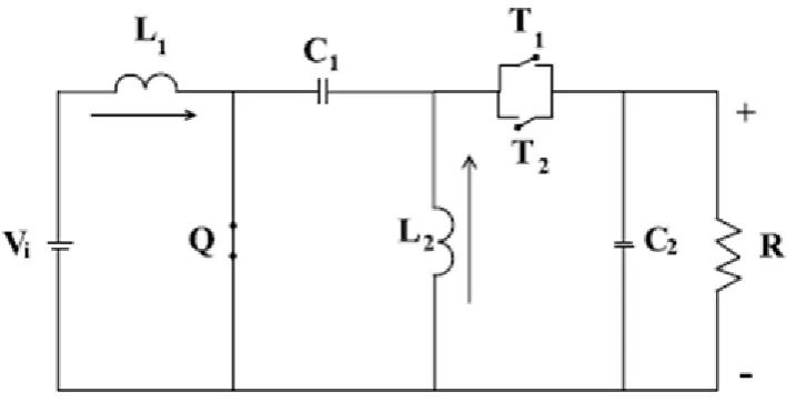
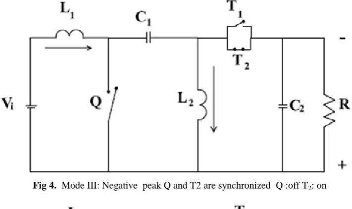
Fig 4. Mode III: Negative peak Q and T2 are synchronized Q :off T2: on
Fig 5. Mode IV: Negative peak Q and T2 are synchronized Q: on T2: off
Fig 2. through Fig 5. shows the different modes of operation and transition from positive to negative peak voltage
The turning on of the synchronizing switch T2 assuages to reverse the direction of the load current and
engage a transition mode to the operation of the system. With the switch Q turned on, the input voltage reappears across L1 with the opposite polarity and allows a linear increase of current to charge the inductor in
the reverse direction. It accompanies a discharge from the capacitor C2 through L2 and the transistor T2 does not
conduct in this mode.
When the switch Q turns off, the input voltage charges the capacitor C1 besides maintaining the current
through the inductor L1.The algebraic difference of the currents through the inductors L1 and L2 contribute to the
output current and produce the negative load voltage.
III.
MODELLING
The philosophy relies on the state space averaging to arrive at a dynamic modeling technique that allows mathematically representing the operation of the converters. It gives the state space representation of each mode of operation and requires taking the average over a cycle for elucidating the complete system. The first two modes give rise to the positive half cycle of output voltage and the remaining two modes to the negative half cycle of output voltage.
It necessitates four equations involving the state variables iL1, iL2, vC1, vC2 to express the operation of the
system. The switch Q remains off and T1 on over the period 1-d where d represents the duty cycle of operation in the first mode.
The Eqns . (1) to ( 4) describe the mode I operation
= + + - (1)
= - (2)
= - (3)
= + + - (4)
The switch Q turns ON and T1 remains on for the period of the chosen duty cycle d in the second mode. The Eqns. 5 to 8 relate to the operation in the mode II = - (5)
= - (6)
= - (7)
= - (8)
The switch Q off and T2 on for the period of 1-d in the third mode of operation. The Eqns. ( 9) to ( 12) represent the behavior in the mode III = + + - (9)
= - (10)
= - (11)
= + - (12)
The switch Q comes back into on state with T2 still on over the period of the duty cycle d to constitute the fourth mode of operation. The Eqns. (13) to (16) explain the operation in the mode IV = - (13)
= - (14)
= - (15)
The averaged state space model of the inverter over a cycle can be obtained using Eqns. 17 and 18 and the corresponding state space matrices from Eqns. (19) to ( 22)
= - (17)
= - (18)
- (19)
- (20)
- (21)
- (22)
The averaged state space matrices relate as:
=
=
=
IV.
CONTROL STRATEGY
The VSC alters the dynamics of a system by the application of a discontinuous control signal in the sense the state feedback control law appears to be a discontinuous function of time and thus allows the system to switch from one continuous structure to another. The discontinuous signal augurs the system to slide along cross section of the system’s normal behavior.
The procedure evolves the design of multiple control structures so that the trajectories travel toward adjacent region with a different control structure in order that the ultimate trajectory does not exist entirely within one control structure and slides along the boundaries of the control structures. The motion of the system that slides along the boundaries forms the locus consisting of the boundaries termed as the switching surface [10].
The function of switching control law allows driving the state trajectory onto a pre-specified surface and maintains it for the subsequent time. It becomes appropriate to formulate a control law that adopts a switching function such as
U = 1 When S>0 U = 0 When S<0
Where S is the instantaneous state variable’s trajectory and can be described as S =α1X1+α2X2 +α3X3
Where α1 , α2 and α3 represent the control parameters usually referred to as the coefficients and X1,
X2and X3 denote the desired state feedback variables that require to be controlled.
The switching surface may be obtained by enforcing S=0.
The mapping for the equivalent control function in terms of the duty ratio control d is given in
Fig 6. Sliding mode controller for Micro grid Inverter
= d d = = d * = βVin - (24)
= = -βL [( +LC ( - βVo) + β(Vo- Vi) - (25)
= - + ( – βVo) + β(Vo- Vi) - (26)
= βL & = LC - (27)
V.
SIMULATION RESULTS
The exercise endeavors to examine the performance of the inverter through simulation on a MATLAB – SIMULINK platform. The Tables 1 and 2 include the specifications of the PV panel and the parametric values of the elements in the inverter.
The study envisages arriving at a steady state sinusoidal output of 230V from a dc input supply of 140V acquired from the solar panel to support a resistive load of 2.5 kW, when the power switches operate at a switching frequency of 10 KHz.
Table 1. Specification for the PV Panel PV Module
Number of cells in a modules 36
Open circuits voltage 21 V
Short circuit current 6.4 A
Voltage at MPP, Vm 17 V
Current at MPP, Im 5.4 A
PV Array Voltage at MPP, Vmpp =Vpv
140
Power at MPP, Pmpp = Ppv
2000W
Current at MPP, Impp = Ipv
13.3 A
No. of Series Modules Ns
Vamp/Vim=9
Table 2. List of Parameters
Description Parameter Nominal Value
Input Voltage Vin 140 V
Inductance L1 & L2
165µH
Capacitance C1 & C2
30 µF
Switching
Frequency F
10KHz
Load Resistance R 2.5KW
Output Voltage Vo 230 V
The efforts relate to simulating the performance in an attempt to obtain 230 volts ac from a solar input of 140 volts. The graphs in Fig 7 and Fig 8 correspond to the input voltage , the output voltage and current corresponding to a load of 2.5 kW. It engages to introduce sudden changes in the load and supply at t = 0.05 s and t = 1 s respectively in order to evaluate the robustness of the controllers. Though the load current increases, still it retains the desired output voltage on account of the modification in the duty cycle. Similarly the VSC ensures to maintain the output voltage even in the case offset point changes as seen from the same figure.
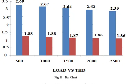
The THD spectrum drawn in Fig 9 and Fig 10 for the same operating point and the bar diagram in Fig 11 elicits the merits of the VSC over the PI controller in terms of a much lower THD for the entire operating
range.
Fig 7. Output voltage and current from PI in Boost Mode
Fig 9. FET for PI in Boost Mode Fig 10. FET for SMC in Boost Mode
Fig 11. Bar Chart
VI.
HARDWARE
IMPLEMENTATION
The methodology involves constructing a hardware prototype with similar ratings as that used in simulation and investigating the performance through the same operating range.It features using a ATmega 8 processor to generate the PWM pulses for the MOSFET switches in accordance with the design of the control strategy.
purpose working registers. The registers remain directly connected to the Arithmetic Logic Unit (ALU), allowing two independent registers to be accessed in one single instruction executed in one clock cycle.
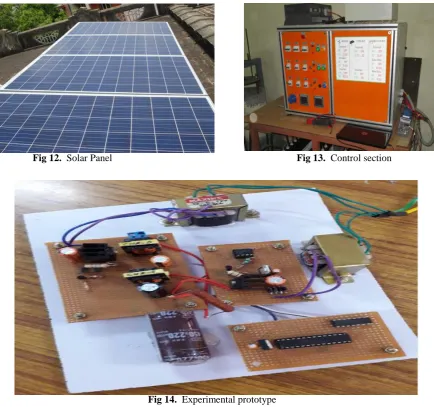
Fig 12. Solar Panel Fig 13. Control section
Fig 14. Experimental prototype
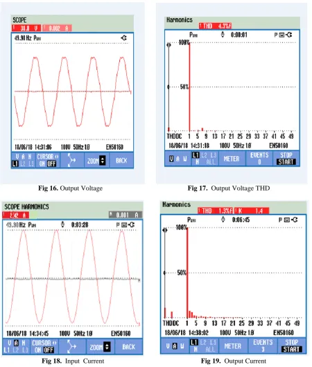
The photographs displayed in Fig 12 through Fig 14 shows the solar PV panel, control section from where the dc output enters the prototype and the hardware set up formed for testing the applicability of the scheme. The flow schematic in Fig 15 explains the process of generation of appropriate firing pulses for the MOSFET switches. The sinusoidal nature of the output voltage in Fig 16 captured using an attenuator probe of 1:10 at the operating point of 2.5kW along with its corresponding THD spectrum in Fig 17 orchestrate the benefits of the chosen inverter in terms of its suitability for being connected to the grid.
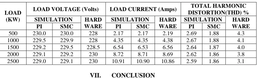
Besides the shape o the input current waveform and its THD spectrum in Fig 18 and 19 respectively, obtained at the same operating point bring out the merits of the control scheme in being able to contribute to the improvement in power quality. The close comparison of the readings in the Table 3 allows validating the simulated performance across the operating range.
Fig 16. Output Voltage Fig 17. Output Voltage THD
Table 3. Comparison of Simulation and Hardware Results
VII.
CONCLUSION
A VSC based control strategy has been formulated for operating the micro-grid inverter from a solar source. The inverter has been modeled in the state space framework and the control theory incorporated to develop the methodology for generating the PWM pulses. The performance has been evaluated to regrates a regulated output voltage over a range of operating loads. The ability of the control scheme has been projected to reject both servo and regulatory disturbances and maintain the desired output voltage at the new operating point. The methodology has been tailored to lower the output voltage and the input current. The consequent increase in the fundamental component has been projected to facilitate the sinusoidal shape of the output voltage. The results have been obtained to enable the inverter claim an integral part of a renewable energy supported micro-grid.
ACKNOWLEDGEMENT
The authors thank the authorities of the DST for providing the necessary facilities through the FIST program in the Energy conversion Lab of the Department of Electrical Engineering at Annamalai University to accomplish this piece of work.
REFERENCES
[1]. G. R .Walker and P. C .Sernia, Cascaded DC-DC converter connection of photovoltaic module, IEEE Transactions on Power Electronics,vol.19,no.4, pp.1130-1139, July 2004.
[2]. A .Fatemi, M. Azizi, K. Rahmani, M. Mohamadian, A.Yazdian, A novel reduced switch count multilevel
AC/AC converter, 19th Iranian Conference on Electrical Engineering,vol.1,pp.17-19,May 2011.
[3]. S .B.Kjaer, J .K. Pedersen and F.Blaabjjer, A review of single phase grid connected inverters for
photovoltaic modules, IEEE Transactions on Industry Applications,vol.41,no.5,pp.1292-1306, 2005.
[4]. Z.Yang and P.C Sen, A novel switch-mode DC to AC inverter with non-linear robust control ,IEEE Transactions on Industrial Electronics,vol.45, pp.602-608, Aug 1998.
[5]. H. Zhang, A.Von Jouanne, S. Dai , A Reduced-Switch Dual-Bridge Inverter Topology for the Mitigation
of Bearing Currents, EMI, and DC Link Voltage Variations,IEEE Transactions Industry
Applications,vol.37,no. 5, pp. 1365-1372, 2001.
[6]. T .Boller, R. M. Kennel, J. Holtz, Increased power capability of standard drive inverters by sequential switching, IEEE International Conference on Industrial Technology, pp.769-774, May 2010.
[7]. V .K. Nikhil and K. D. Joseph, A reduced switch multilevel inverter for harmonic reduction, IEEE Power and Energy Engineering Conference,pp.1-4,2012.
[8]. KB Siddesh and GS Rajanna, Chattering Reduction in Sliding Mode Controlled DC-DC Buck Converter
Based on a New Novel Reaching Law, European,Journal of Advances in Engineering and Technology,vol.10,no.2,pp.12-16,2015.
[9]. R .L. Cardoso and I..Barbi ,Bi-Directional DC-AC converters with high frequency Isolation,
International Symposium on Signals, Circuits and Systems,2005.
[10]. G. H.Tan, J. Z. Wang and Y. C. Ji, Soft-switching flyback inverter with enhanced power decoupling for photovoltaic applications, IET Electric Power Applications, vol.1, no.2, March 2007.
[11]. P. C. Loh, P .C. Tan, F. Blaabjerg, Topological Development and Operational Analysis of Buck-Boost Current Source Inverters for Energy Conversion Applications, IEEE Power Electronics Specialists Conference,2006.
[12]. Adda Ravindranath, Santanu K. Mishra and Avinash Joshi, Analysis and PWM control of switched Boost
inverter ,IEEE Transactions on Industrial Electronics ,Vol.60,no.12,December 2013
[13]. R. Senthil Kumar, S. Selva Kumar and V. Suresh, Transformer less grid connected SEPIC converter for
photovoltaic generation systems, International Journal of Innovative Research in Advanced
Engineering,vol.1,no. 4,May 2014
LOAD (KW)
LOAD VOLTAGE (Volts) LOAD CURRENT (Amps) TOTAL HARMONIC DISTORTION(THD) %
SIMULATION HARD
WARE
SIMULATION HARD
WARE
SIMULATION HARD
WARE
PI SMC PI SMC PI SMC
500 230.0 230.0 228 2.17 2.17 2.19 2.69 1.88 4.3
1000 229.5 229.9 228 4.35 4.35 4.38 2.67 1.88 4.1
1500 229.2 229.5 228.5 6.54 6.53 6.56 2.64 1.87 4.0
2000 229.1 229.2 230 8.72 8.71 8.69 2.62 1.86 3.8
[14]. P. Sivaraman and Dr. A. Nirmalkumar , PV Array Fed SEPIC and VSI Based Power Conversion System for Single Phase Induction Motor Drive, International Journal of Modern Engineering Research,vol.2, no.3, pp.1181-1188, 2012.
[15]. Rong Chen, Jia-Sheng Zhang, Wei Liu and Chang-Ming Zheng, Half Load-Cycle Worked Dual SEPIC
Single - State Inverter, Journal of Electrical Technology, vol., No. 1, pp 143-149, 2016.