DIN EN ISO 9001:2000 certified
Edition: 01.07 - 05/2008
ADDI-DATA GmbH
Airpark Business Center
Airport Boulevard B210
77836 Rheinmünster
Germany
Technical support:
+49 7229 1847– 0
Technical description
PC104-PLUS1500
Warranty and liability
The user is not permitted to make changes to the product beyond the intended use, or to interfere with the product in any other way.
ADDI-DATA shall not be liable for obvious printing and phrasing errors. In addition, ADDI DATA, if legally permissible, shall not be liable for personal injury or damage to materials caused by improper installation and/or commissioning of the board by the user or improper use, for example, if the board is operated despite faulty safety and protection devices, or if notes in the operating instructions regarding transport, storage, installation, commissioning, operation, thresholds, etc. are not taken into
consideration. Liability is further excluded if the operator changes the board or the source code files without authorisation and/or if the operator is guilty of not monitoring the permanent operational capability of working parts and this has led to damage.
Copyright
This manual, which is intended for the operator and its staff only, is protected by copyright. Duplication of the information contained in the operating instructions and of any other product
information, or disclosure of this information for use by third parties, is not permitted, unless this right has been granted by the product licence issued. Non-compliance with this could lead to civil and criminal proceedings.
ADDI-DATA software product licence
Please read this licence carefully before using the standard software. The customer is only granted the right to use this software if he/she agrees with the conditions of this licence.
The software must only be used to set up the ADDI-DATA boards.
Reproduction of the software is forbidden (except for back-up and for exchange of faulty data carriers). Disassembly, decompilation, decryption and reverse engineering of the software are
forbidden. This licence and the software may be transferred to a third party if this party has acquired a board by purchase, has agreed to all the conditions in this licence contract and the original owner does not keep any copies of the software.
Trademarks
- ADDI-DATA is a registered trademark of ADDI-DATA GmbH.
- Turbo Pascal, Delphi, Borland C, Borland C++ are registered trademarks of Borland Insight Company.
- Microsoft C, Visual C++, Windows XP, 98, Windows 2000, Windows 95, Windows NT, EmbeddedNT and MS DOS are registered trademarks of Microsoft Corporation.
- LabVIEW, LabWindows/CVI, DasyLab, Diadem are registered trademarks of National Instruments Corp.
- CompactPCI is a registered trademark of PCI Industrial Computer Manufacturers Group. - VxWorks is a registered trademark of Wind River Systems Inc.
WARNING
The following risks result from improper implementation
and from use of the board contrary to the regulations:
♦
Personal injury
♦
Damage to the board, PC and peripherals
♦
Pollution of the environment
♦
Protect yourself, the others and the environment!
♦
Read carefully the safety precautions
(yellow leaflet).
If this leaflet is not with the documentation, please contact us
and ask for it.
♦
Observe the instructions of the manual.
Make sure that you do not forget or skip any step. We are not
liable for damages resulting from a wrong use of the board.
♦
Used symbols:
i
IMPORTANT!
designates hints and other useful information.
WARNING!
It designates a possibly dangerous situation.
If the instructions are ignored the board, PC and/or peripheral may
be destroyed.
1
DEFINITION OF APPLICATION ...
28H7
1.1 Intended use ...29H7
1.2 Usage restrictions...30H7
1.3 General description of the board ...31H7
2
USER ...
32H9
2.1 Qualification ...33H9
2.2 Personal protection...34H9
3
HANDLING OF THE BOARD...
35H10
4
TECHNICAL DATA ...
36H11
4.1 Electromagnetic compatibility (EMC) ...37H11
4.2 Physical set-up...38H11 4.3 Limit values...39H12 4.3.1 Energy requirements ...40H12 4.3.2 Power loss ...41H13 4.3.3 Digital inputs...42H13 4.3.4 Digital outputs ...43H13 4.3.5 Timer/Watchdog ...44H14 4.3.6 Counter...45H14 4.4 Component scheme...46H15
5
INSTALLATION OF THE BOARD ...
47H17
5.1 First steps...48H17
5.2 Board insertion into a housing/system ...49H17
5.2.1 Switch off the housing/system and all units connected to the housing/system ...50H18
5.2.2 Fastening the board ...51H18
6
SOFTWARE ...
52H20
6.1 Board registration ...53H21
6.1.1 Installation of a new board ...54H21
6.1.2 Changing the registration of a board ...55H23
6.2 Questions and software downloads on the internet ...56H26
7
CONNECTION TO THE PERIPHERAL ...
57H27
7.1 Connection to the screw terminal panels and relay output board...58H27
Contents PC104-PLUS1500
8
FUNCTIONS OF THE BOARD ...
60H30
8.1 Block diagram...61H30
8.2 Overview: Description of the board functions ...62H30
8.3 Digital inputs ...63H31 8.4 Digital outputs...64H32 8.5 Interrupt...65H33 8.6 Watchdog/timer ...66H36 8.6.1 Timer1/Digital watchdog...67H36 8.6.2 Timer2...68H36 8.7 Counter ...69H36
9
STANDARD SOFTWARE ...
70H39
9.1 Software functions...71H39 9.2 Software samples...72H4210
APPENDIX ...
73H43
10.1 Glossary ...74H4311
INDEX ...
75H48
Figures
0H
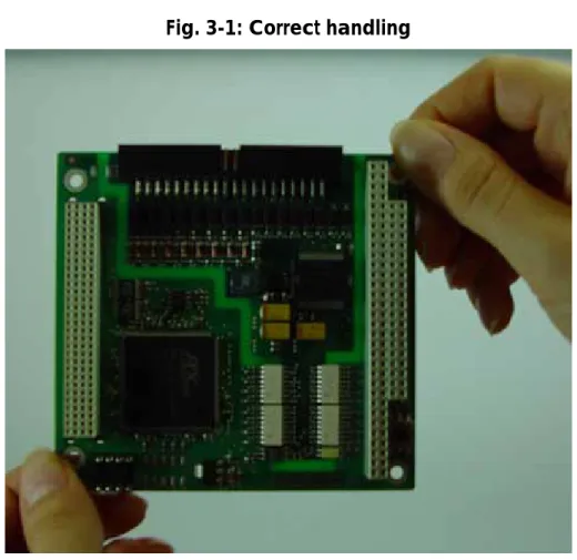
Fig. 3-1: Correct handling...76H10
1H
Fig. 4-1: Physical set-up ...77H11
2H
Fig. 4-2: Component scheme (top layer)...78H15
3H
Fig. 4-3: Component scheme (bottom)...79H16
4H
Fig. 5-1: Setting the turn switch ...80H17
5H
Fig. 5-2: Connector with PCI-/ISA signals...81H18
6H
Fig. 5-3: Fastening the board ...82H19
7H
Fig. 6-1: New inserted board ...83H21
8H
Fig. 6-2: ADDevice Manager ...84H22
9H
Fig. 6-3: ADDIREG registration program (example) ...85H23
10H
Fig. 7-1: Connection of the PC104-PLUS1500 to the PX 901-DG or PX 9000 ...86H27
11H
Fig. 7-2: Connection of the PC104-PLUS1500 to the relay output board PX 8500 ...87H28
12H
Fig. 7-3: 40-pin header...88H29
13H
Fig. 7-4: Ribbon cable FB104-1500 from pin header to 37-pin male connector...89H29
14H
Fig.8-1: Block diagram of the PC104-PLUS1500 ...90H30
15H
Fig. 8-2: Digital input level...91H31
16H
Fig. 8-3: Digital output level ...92H33
17H
Fig. 8-4: Example for the OR logic: Edge switch interrupt ...93H35
18H
Fig.8-5: Upwards counter...94H37
19H
Fig. 8-6: Downwards counter...95H38
Tables
20H
Table 4-1: Power loss ...96H13
21H
Table 5-1: Position of the turn switch ...97H17
22H
Table 8-1: OR logic...98H34
23H
Table 8-2: Mode register – Complete overview...99H34
24H
Table 8-3: Mode register – partial overview ...100H34
25H
Table 8-4: Principle of the OR logic ...101H35
26H
PC104-PLUS1500 Definition of Application
1
DEFINITION OF APPLICATION
1.1
Intended use
The board PC104-PLUS1500 must be inserted in a PC/104-Plus system with PCI slot, which is used as electrical equipment for measurement, control and
laboratory pursuant to the norm IEC 61010-1.
1.2
Usage restrictions
The PC104-PLUS1500 board must not to be used as safety related part for securing emergency stop functions.
The PC104-PLUS1500 board must not be used in potentially explosive atmospheres.
1.3
General description of the board
Data exchange between digital data between the board PC104-PLUS1500 and the peripheral is to occur through a shielded cable. This cable must be connected to the 37-pin SUB-D male connector.
The board has 16 input channels and 16 output channels 16 output channels for processing digital signals.
The use of the board PC104-PLUS1500 in combination with external screw terminal panels is to occur in a closed switch cabinet.
The screw terminal panel PX901-DG allows the connection of digital signals to the peripheral through the cable ST010.
The connection with our standard cable ST010 complies with the following specifications:
- metallized plastic hoods - shielded cable
- cable shield folded back and firmly screwed to the connector housing.
The use of the board in a PC/104 system could change the features of the system regarding noise emission and immunity. Increased noise emission or decreased noise immunity could result in the system not being conform anymore.
Check the shielding capacity of the system housing and of the cable prior to putting the device into operation.
The use of the board according to its intended purpose includes observing all advises given in this manual and in the safety leaflet.
Uses beyond these specifications are not allowed. The manufacturer is not liable for any damages which would result from the non-observance of this clause. Make sure that the board remains in its protective blister pack until it is used.
Do not remove or alter the identification numbers of the board. If you do, the guarantee expires.
PC104-PLUS1500 User
2
USER
2.1
Qualification
Only persons trained in electronics are entitled to perform the following works: - installation
- use
- maintanance.
2.2
Personal protection
Consider the country-specific regulations about: - the prevention of accidents
- electrical and mechanical installations - radio interference suppression.
3
HANDLING OF THE BOARD
PC104-PLUS1500 Technical data
4
TECHNICAL DATA
4.1
Electromagnetic compatibility (EMC)
The PC is to comply with the norm IEC61326 for measurement, control and laboratory use and with the specifications for EMC protection.
The board has been subjected to EMC tests in an accredited laboratory. The board complies with the limit values set by the norms IEC61326 as follows:
True value Set value ESD (Discharge by contact/air) ... 4/8 kV 4/8 kV Fields... 10 V/m 10 V/m Burst ... 4 kV 2 kV Conducted radio interferences ... 10 V 10 V
4.2
Physical set-up
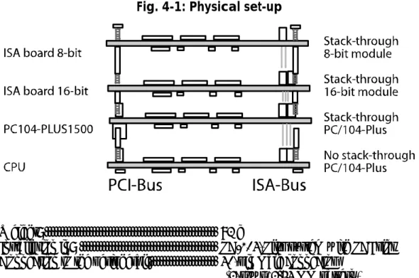
i
IMPORTANT!
When inserting the board into the system, please insert firstly
the PCI boards and then additional ISA boards.
The following figure (103HFig. 4-1) shows how the board PC104-PLUS1500 is
inserted into a system. Furthermore the example show additionally inserted boards.
Fig. 4-1: Physical set-up
Weight: ... 92 g
Installation in: ... PC/104-Plus system with PCI slot Connection to the peripheral:... 40-pin male connector
Accessories0F
1:
Cables (for screw terminal panel): ...FB104-1500 40-pin on 37-pin SUB-D connector
Standard cable ST010
Cables (for relay output board): ... Standard cable ST021 between FB104-1500 and PX 8500-G
Standard cable ST022 between
PX 8500-G and PX 901-DG Screw terminal panel: ...PX 901-DG
PX 9000 Relay output board: ...PX 8500-G
WARNING!
The supply lines must be installed safely against mechanical
loads.
4.3
Limit values
Max. altitude: ... 2000 m above sea level Operating temperature: ... 0 to 60°C
Storage temperature: ... -25 to 70°C Relative humidity at indoor installation
50% at +40 °C 80% at +31 °C
Minimum PC requirements: PCI BIOS from Version 1.0
Bus speed: ...≤ 33 MHz
Operating system: ... Windows Vista (32-bit), XP 2000,
Linux
4.3.1
Energy requirements
Current consumption: ... See table below PC104-PLUS1500
+ 3.3 V from PC 95 mA 0.314 W + 5 V from PC 45 mA 0.225 W
PC104-PLUS1500 Technical data
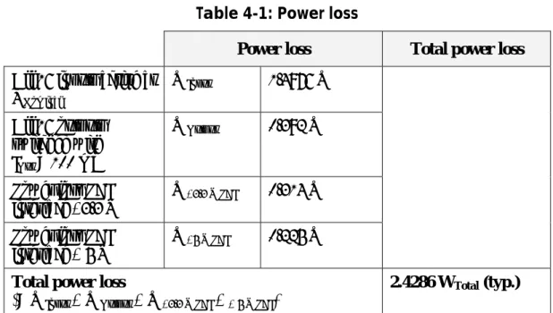
4.3.2
Power loss
Table 4-1: Power loss
Power loss Total power loss All 16 inputs active at
UNominal WInput 1.4976 W All 16 outputs switched with IOut = 100 mA WOutput 0.392 W
Power loss PCI interface +3.3 V
W+3.3 V PCI 0.314 W Power loss PCI
interface + 5 V
W+5 V PCI 0.225 W Total power loss
(= WInput + WOutput + W+3.3 V PCI + + 5 V PCI)
2.4286 WTotal (typ.)
4.3.3
Digital inputs
Number: ...16 digital inputs
Of them one channel is used as counter input [channel 0]
Optical isolation: ...1000 V (through opto-coupler) Interruptible channels:...2 channels (channel 3 and 2) Interrupt compare logic:...OR mode (with fixed filter times) Input voltage: ...Up to 30 V
Nominal voltage:...Unom = 24 V
Input current (channel 1-15): ...3.9 mA at 24 V, typ. Input current (channel 0):...6 mA at 24 V
Input frequency (max.):...Channel (0): 100 KHz (at 24 V) Input frequency (max.):...Channel (15-1): 5 KHz (at 24 V) Logic input levels:
UH (max.) ...30 V / 6 mA (typ.) UH (min.): ...19 V / 2 mA (typ.) UL (max.):...14 V / 0.7 mA (typ.) UL (min.): ...0 V / 0 mA (typ.) Filter for interruptible channels:...40 μs
4.3.4
Digital outputs
Number: ...16 digital outputs
Optical isolation: ...1000 V (through opto-coupler) Output type:...High-Side
(Last on ground according to
IEC 1131-2;
Driver type: Infineon BTS4880R
(8-channel type)
Nominal voltage: ... 24 V
Supply voltage range: ... 11 V to 36 V
Current limit: ... 1.5 A per 8 channels (through PTC) Output current for each output: ... 150 mA (typ.)
Short circuit current for each output:... 1.1 A (typ.) pulse current Shut-Down at 24 V, Rload<0.1 R RDS ON (max.):... 0.2 Ohm at 25 °C
Turn-on time (typ.): ... 50 μs Turn-off time (typ.): ... 75 μs Overtemperature (Shut-Down):... 135 °C Temperature hysteresis:... 10 °C
Diagnostics: ... Common diagnostic bit for all 16 Channels at overtemperature of one
channel
4.3.5
Timer/Watchdog
Timer1 (with watchdog)
Number:... 1 Timer/watchdog depth:... 12-bit
Programmability of the timer: Programmable as watchdog for the digital outputs Time bases:... µs, ms, s Monitoring period: ... 1 to 4095 µs, ms, s Tolerance: ... ≤ 1 µs, ms, s Timer2 Number:... 1 Timer depth: ... 12-bit Time bases: ... µs, ms, s
Monitoring period: ... 1 to 4095 µs, ms, s Tolerance: ... ≤ 1 µs, ms, s
4.3.6
Counter
Number:... 1 Counter depth: ... 16-bit Signal channel: ... Channel 0
Reload value: ... Programmable through software Upwards/Downwards counter: ... Programmable through software Limit frequency: ... 100 KHz
PC104-PLUS1500 Technical data
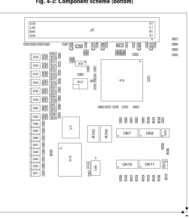
4.4
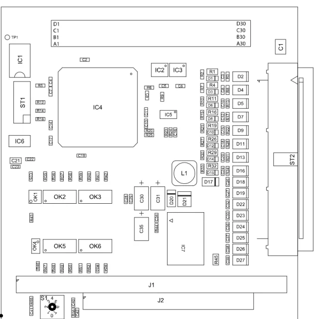
Component scheme
PC104-PLUS1500 Installation of the board
5
INSTALLATION OF THE BOARD
5.1
First steps
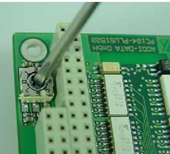
Before beginning with the installation of the board, please ensure that the turn switch (see 104HFig. 5-1) is set correctly. Set the turn switch in the way that it matches
the position of the board PC104-PLUS1500 on the CPU (see 105HTable 5-1)
Table 5-1: Position of the turn switch Position of the PC104-PLUS1500 on the
CPU
Position of the turn switch
PC104-PLUS1500 is the 1. board on CPU 0 (alternatively 4*) PC104-PLUS1500 is the 2. board on CU 1 (alternatively 5) PC104-PLUS1500 is the 3. board on CPU 2 (alternatively 6) PC104-PLUS1500 is the 4. board on CPU 3 (alternatively 7)
* State of delivery ♦Check if the turn switch is set correctly (see table above)
If the setting is correct, you can continue with the installation (see 106HFig. 5-1):
♦Set the turn switch to the correct position with a screw driver Fig. 5-1: Setting the turn switch
5.2
Board insertion into a housing/system
The following sections describe the board insertion into the housing/system of any manufacturer. Therefore, the following part is only a general overview as it does not consider the differences when inserting it into the housings/systems of other manufacturers. Thus, please do observe also the instruction of your
5.2.1
Switch off the housing/system and all units connected to
the housing/system
♦Pull the housing/system mains plug from the socket
♦Open the housing/system as described in the manual of the manufacturer ♦Follow the instructions of the manufacturer
5.2.2
Fastening the board
♦Select an adequate slot
♦Plug the board onto the respecting slot
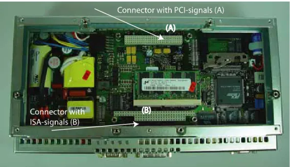
Fig. 5-2: Connector with PCI-/ISA signals1F
1
1 In the picture a SIMATIC Microbox PC 420 was used
i
IMPORTANT!
You must observe the safety instructions, in the present manual,
in the yellow leaflet (safety precautions) and the instructions of
your housing/system manufacturer.
PC104-PLUS1500 Installation of the board
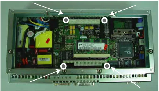
Fig. 5-3: Fastening the board
♦Fix the board with four screws or spacer bolts2F1
i
IMPORTANT!
The instructions in the present manual respecting the
installation of the board are only generally described. Thus,
follow also the individual instructions of your housing/system
manufacturer.
If you want to insert a further board:
♦Plug an extension frame or something similar as described in manual of the manufacturer of the housing/system
i
IMPORTANT!
Observe the max. number of boards that can be inserted into the
housing/system of the respecting manufacturer.
If you do not want to insert any further boards:
♦Close the housing/system as described in the manual of the system/housing manufacturer
1
6
SOFTWARE
In this chapter you will find a description of the delivered software and its possible applications.
i
IMPORTANT!
Further information for installing and uninstalling the different
drivers is to be found in the delivered description
"Installation
instructions for the PCI and ISA bus".
Please note that the
installation with a PC/104-Plus-system can differ from the
standard installation (with PCI or ISA bus).
A link to the corresponding PDF file is available in the navigation pane (Bookmarks) of Acrobat Reader.
i
IMPORTANT!
The supported software functions for the
PC104-PLUS1500
listed in chapter
107H9.
The board is supplied with a CD-ROM containing the ADDIPACK software package for Windows NT 4.0 and Windows XP/2000/98.
ADDIPACK is composed of following programs:
- ADDIREG: The ADDIREG registration program is a 32-bit program for Windows NT 4.0 and Windows XP/2000/98. The user can register all hardware information necessary to operate the ADDI-DATA PC boards.
- ADDIDRIVER contains API functions to operate the ADDI-DATA boards in 32 bits.
- ADDevice Manager configures the resources of the ADDI-DATA virtual board (See below).
- ADDI-DATA virtual board:
ADDI-DATA software is based on the principle of a virtual board: it
transposes the different functions (e.g. digital inputs, analog outputs, timer, ...) of all inserted ADDI-DATA boards as the functions of a single (virtual) board. The virtual board features a pool of functions, the functionality of which can be called up without calling a specific board.
- ADDEVICE MAPPER was specifically developed for the ADDIPACK boards to facilitate the management of the virtual board. With this program you can optimally adapt the virtual board to your application requirements.
IMPORTANT!
For some functions of the ADDEVICE MAPPER program the browser Internet Explorer 6 or higher has to be installed on your PC.
PC104-PLUS1500 Software
6.1
Board registration
When starting the set-up of ADDIREG, the PC104-PLUS1500 is automatically recognised and registered.
6.1.1
Installation of a new board
If a new board is recognised, the following window is displayed: Fig. 6-1: New inserted board
The boards which have been removed from the PC since the last ADDIREG start are listed in the upper table
The new inserted boards are listed in the lower table.
In case further information is required for the operation of the board, click on "More Information". ADDevice Manager is started.
ADDevice Manager
Fig. 6-2: ADDevice Manager
The following parameters are displayed for every inserted board: First column:
- Board name
- Board index: Number allocated to the board when it is registered in ADDIREG.
- Slot number - IRQ line
- Different addresses which are automatically allocated to the board by the BIOS.
Other columns:
The program distinguishes between the resources (Analog/digital input/output, watchdog, ...) of the virtual board (V, software) and the real board (R, board). The following parameters are listed
- Module number, - Number of resources
- Index: The first index line represents the number of the first resource (left: virtual resource - right: real board) The second index line represents the number of the last resource (left: virtual resource - right: real board). - Type (24 V/5 V, voltage/current, HS/OC - High-Side/Open collector).
- IRQ: if the input channels are interruptible, the program displays the number of the first and of the last input channel
PC104-PLUS1500 Software By clicking twice within a column, the connection principle and the technical data
of the resource are displayed. This function is only possible if a question mark appears with the cursor.
You can export the set configuration as a text file. Click on "file" and save the configuration as a .txt file with "Export information to file...". You can then print the configuration or use it for other boards.
Once you have controlled the registration, you can quit the window of ADDevice Manager. The board is ready to operate.
6.1.2
Changing the registration of a board
You can change the current board configuration with ADDIREG Description of the ADDIREG program
The program is automatically installed with ADDIPACK.
Start ADDIREG under Start/Programme/ADDIPACK/ADDIREG.
i
IMPORTANT!
First quit all the applications (programs) which use the board
before starting the ADDIREG program.
In the main window of ADDIREG the fields "Insert" and "Clear" are not available for the board.
Table:
Board name:
Names of the different registered boards (e.g.: APCI-3200). Base address:
Selected base address of the board. For PCI boards the base address is allocated through BIOS.
Access:
Selection of the access mode for the ADDI-DATA digital boards. Access in 8-bit or 16-bit or 32-bit mode.
PCI bus/device/(slot):
Number of the used PCI bus, slot, and device. If the board is no PCI board, the message "NO" is displayed.
Interrupt:
Used interrupt of the board. If the board supports no interrupt, the message "Not available" is displayed. For PCI boards the interrupt is allocated through BIOS.
DMA (ISA boards only):
Indicates the selected DMA channel or "Not available" if the board uses no DMA or if the board is no ISA board.
More information:
Additional information like the identifier string or the installed COM interfaces. It also displays whether the board is programmed with ADDIDRIVER or if a PCI DMA memory is allocated to the board.
Text boxes:
Base address name:
Description of the used base addresses for the board. Select a name through the pull-down menu. The corresponding address range is displayed in the field below (Base address).
Interrupt name:
Description of the used IRQ lines for the board. Select a name through the pull-down menu. The corresponding interrupt line is displayed in the field below (Interrupt).
DMA name (for ISA boards only):
When the board supports 2 DMA channels, you can select which DMA channel is to be changed.
DMA channel (for ISA boards only): Selection of the used DMA channel.
PC104-PLUS1500 Software
Buttons:
Edit:
Selection of the highlighted board with the different parameters set in the text boxes.
Set:
Sets the parametered board configuration. The configuration should be set before you save it.
Cancel:
Reactivates the former parameters of the saved configuration. Default:
Sets the standard parameters of the board.
More information (not available for the boards with ADDIPACK)
You can change the board specific parameters like the identifier string, the COM number, the operating mode of a communication board, etc...
If your board does not support this information, you cannot activate this button. ADDIDriver Board Manager:
Under Edit/ADDIDriver Board Manager you can check or change the current settings of the board set through the ADDEVICE Manager.
ADDevice Manager starts and displays a list of all resources available for the virtual board.
Test registration:
Controls if there is a conflict between the board and other devices installed in the PC. A message indicates the parameter which has generated the conflict. If no conflict has occurred, "Test of device registration OK" is displayed.
Deinstall registration:
Deinstalls the registrations of all boards listed in the table and deletes the entries of the boards in the Windows Registry.
Print registration:
Prints the registration parameter on your standard printer. Quit:
Registration test
Under "Test registration" you can test if the registration is "OK".
This test controls if the registration is right and if the board is present. If the test has been successfully completed you can quit the ADDIREG program. The board is initialised with the set parameters and can now be operated.
In case the registration data is to be modified, it is necessary to boot your PC again. A message asks you to do so. When it is not necessary you can quit the ADDIREG program and directly begin with your application.
6.2
Questions and software downloads on the internet
Do not hesitate to e-mail us your questions.per e-mail: [email protected] or
[email protected] Free downloads of standard software
You can download the latest version of the software for the board PC104-PLUS1500:
27H
http://www.addi-data.com
i
IMPORTANT!
Before using the board or in case of malfunction during
operation, check if there is an update of the product (technical
description, driver). The current version can be found on the
internet or contact us directly.
PC104-PLUS1500 Connection to the peripheral
7
CONNECTION TO THE PERIPHERAL
You can connect the board to screw terminal panels (see 108HFig. 7-1) or to a relay
output board (see 109HFig. 7-2).
7.1
Connection to the screw terminal panels and relay
output board
Fig. 7-1: Connection of the PC104-PLUS1500 to the PX 901-DG or PX 9000
Fig. 7-2: Connection of the PC104-PLUS1500 to the relay output board PX 8500
PC104-PLUS1500 Connection to the peripheral
7.2
Connector pin assignment
Fig. 7-3: 40-pin header
Fig. 7-4: Ribbon cable FB104-15003F
1 from pin header to
37-pin male connector
1
8
FUNCTIONS OF THE BOARD
8.1
Block diagram
Fig.8-1: Block diagram of the PC104-PLUS1500
8.2
Overview: Description of the board functions
The board PC104-PLUS1500 allows the parallel input/output of digital signals in 24 V industry level environments.
Peripheral and system are optically isolated at the same time. Available functions:
- 16 digital inputs: Two of them are interruptible - 16 digital outputs:
- Short circuit resistance against load - Protection against overtemperature - Reduced ON-resistanc
- Broad supply voltage range
- Switching-off if the voltage falls under the limit value (7 V typ.) - 2 timers (12-bit)
Of which one timer can be used as watchdog - 1 counter (16-bit)
PC104-PLUS1500 Functions of the board The base address and the interrupt are set automatically through the BIOS.
EMC: Design in accordance with the CE regulations
8.3
Digital inputs
The board has 16 digital input channels. Two of them are interruptible. One channel is used as counter input channel [channel 0].
The inputs acquire external signals: The input information is loaded, by the driver functions, as numerical value into a memory cell of the system.
This numerical value calculates the status of the input signals.
All inputs have a common current ground: Digital input GND (inputs), pin 19 of the 40-pin header.
The input current is at 3.9 mA for channels 1-15 and at 6 mA for channel 0 at UNominal. The maximal input voltage is 30 V.
Logic "1": Input voltage at the 40-pin header is superior to 19 V. Logisch "0": Input voltage at the 40-pin header is inferior to 14 V.
WARNING!
If you operate all inputs with the same voltage supply,
the voltage supply
must supply the corresponding current.
The maximal input voltage is at 30 V.
Transil diodes, Z diodes, C filter and opto-couplers protect the system bus against noise emitted by the peripheral. Thus, the effects of inductive and capacitive noises are reduced.
For the interruptible inputs and the counter channel additional digital filters are implemented.
The board requires no initialisation to read the 24 V digital information. After successful Power ON Reset the data is immediately available on the board.
8.4
Digital outputs
The board has 16 digital output channels (24 V High Side).
Positive logic is used
- logic "1": Setting the output through software (switch on ON), - logic "0": Resetting the output (switch on OFF).
The outputs (switch) switch the +24 V ext. outside to the load. One end of the load is connected to the ground of 0 V EXT (output. All outputs have a common ground line: (0 V EXT (outputs) at the 40-pin header.
WARNING!
If you operate all outputs with the same voltage supply,
the voltage
supply must deliver at least the power that is required for your
application.
The maximum supply voltage is 36 V. Each output can switch max. 150 mA current. The current is limited for each 8 outputs on 1 A by a self-resetting fuse.
Characteristics of the outputs:
- Short-cirucit proof against load. The output is switched off
- Protection against overtemperature: The power unit is switched off, i.e. each 8 channels: 0 to 7 and 8-15
- The outputs are switched off if the supply voltage drops - Diagnostic report: Short-circuit, overtemperature
- The outputs allow the switching of ohmic, capacitive and inductive loads Transil diodes, C filter and opto-coupler filter noise from the peripheral to the systembus. Thus, the effect of inductive and capacitive noise is reduced. Possible noise emissions are also reduced by C filters.
The board requires no initialisation to indicate the 24 V digital information. You can program the outputs right after Power ON Reset.
Status after Power ON Reset: All outputs are reset (switch on OFF).
Special functions
Two diagnostic bits are available.
The CC-diagnostics (ϑ-diagnostic) calculates: - If an output is short-circuited or
if there is overtemperature on an output driver The Vcc-diagnostics calculates:
PC104-PLUS1500 Functions of the board This error information is available for the user through an interrupt routine. Please
find further information in the software description “Interrupt”, which is available as a separate PDF file.
Fig. 8-3: Digital output level
8.5
Interrupt
The board PC104-PLUS1500 has one interrupt line. You can select which interrupt of the PCI bus is used by setting the turn switch (see 110HFig. 5-1).
Possible interrupt sources :
- Interruptible inputs (channel 2 and 3) - Timer1/watchdog run down
- Timer2 run down - Counter overflow
- Watchdog run down, outputs are reset
- Voltage error (external voltage supply is not available) - Short-circuit error, overtemperature error
The interrupt source information is available for the user program through an interrupt routine. Please find further information in the software description „Interrupt“, which is available as a separate PDF file.
Interruptible inputs: IRQ logic
It is possible to mask an OR event (Event) at rising/falling edge.
For the control of the IRW logic the following functions are available (set by software):
- enable/disable of the interrupt function - interrupt source rereadable
- IRQ status register rereadable
- the interrupt function is programmed through two registers, with which the events are masked (Hex):
Mode_1 reacts on rising edges or high levels Mode_2 reacts on falling edges or low levels
Interrupt control
The interrupt logic is blocked after triggering an interrupt. It is released again at the end of the interrupt routine. In the interrupt routine the boards does not react on changes of the input channels. A further interrupt is generated if an
interruptible edge or status change occurs. A new interrupt is firstly possible after the completion of the original interrupt service routine.
OR logic
Table 8-1: OR logic
Disable Rising Falling Rising/falling Mode_1 0 1 0 1 Mode_2 0 0 1 1 The OR logic reacts to rising or falling edges.
An interrupt is triggered if at an interruptible input an edge switch occurs that fulfils the interrupt condition, which is set by Mode_1 and Mode_2.
Table 8-2: Mode register – Complete overview
D31…. D5 D4 D3 D2 D1 D0
Mode_1 Channel 3 Channel 2
Mode_2 Channel 3 Channel 2
Is not used:
Table 8-3: Mode register – partial overview Channel 3 rising Channel 2 rising Channel 3 falling Channel 2 falling Example:
Mode_1 = 0x0000000Chex // Release rising edge (channel 2 to 3) Mode_2 = 0x00000008hex// Release falling edge (channel 3)
In the figure below the following parameters are set: 1. Condition: Channels 2 and 3 react to rising edges
(Mode_1 = 11).
2. Condition: Channels 2 and 3 react to falling edges (Mode_2 = 11).
PC104-PLUS1500 Functions of the board
Fig. 8-4: Example for the OR logic: Edge switch interrupt
Table 8-4: Principle of the OR logic Input 2
Input 3 INPUT 3
MODE2, MODE1 INPUT 2 MODE2, MODE1
0,0 0,0 No interrupt 1,0 0,0 10* 10 0,1 0,0 10 10 1,1 0,0 10 10 10 10 0,0 1,0 01** 01 1,0 1,0 01 10 01 10 0,1 1,0 10 01 10 01 1,1 1,0 10 01 10 10 01 10 0,0 0,1 01 01 1,0 0,1 01 10 01 10 0,1 0,1 01 10 10 01 1,1 0,1 01 10 10 10 01 10 0,0 1,1 01 01 01 01 1,0 1,1 01 01 10 01 01 10 0,1 1,1 01 10 01 10 01 01 1,1 1,1 01 10 01 10 10 01 01 10
* 10: Interrupt source: The second input (channel 3) generated an interrupt. ** 01: Interrupt source: The first input (channel 2) generated an interrupt.
8.6
Watchdog/timer
8.6.1
Timer1/Digital watchdog
The 12-bit Timer1 is a downwards counter, which can generate an interrupt after the reload value has run down (timeout). With the timer, a time base is made available, independently from the system clock, with which e.g. operations can be synchronised.
The status of the counter value as well as the status register and interrupt register can be reread by the software.
Timer1 can be programmed as watchdog, which resets the digital outputs after the run down of its reload value (timeout).
When releasing watchdog, with each setting of the digital outputs, the reload value is loaded newly (triggering). The triggering can be done also directly by software command without the new setting of the digital outputs.
The operation states can be reread. Three different clock signals can be used as time bases for the watchdog.
8.6.2
Timer2
The 12-bit Timer1 is a downwards counter, that can generate an interupt after the run down of the reload value (timeout). With the timer, independently from the PC clock and time base is provided, with which e.g. operations can be
synchronized.
The status of the counter value as well as status and interrupt register can be reread with the software.
8.7
Counter
On the board PC104-PLSU1500 there is 1 x 16-bit counter input, whose function can be compared with the counter component 82C54. The counter can be
programmed over software.
The signal input (clock) of the counter is channel 0. Channel 0 is available as usual digital input, independent from the counter function. The limit frequency is 100 KHz. A signal input for gate and trigger function is not available.
Characteristics of the counter:
- 2 counting modes: The counter is programmed as upwards counter (see a) or downwards counter (see b)
- After reaching the reload value or if the counter has run off, an interrupt can be generated.
PC104-PLUS1500 Functions of the board
- Clock: The counter counts at positive or negative edge or with each edge - Trigger function: Sets the counter on its start value 0 in the
upwards mode = clear function
- Clear function: The counter status is deleted. (counting value set on 0) a) Upwards counter
Function upwards counter:
The counter starts with counter value 0 and increments with each valid edge. At the result of count reload value -1, with the following valid edge the counter is set on 0. An interrupt can be generated with the overflow.
Software clear: Deletes counter (= 0) Software trigger: Sets counter (= 0) Example upwards counter
Reload value = 9
Initialisation on rising edge Interrupt is released
At the current result of count = 8 (reload value -1) with the following valid edge the counter is deleted and the interrupt enabled, i.e. after reaching the reload value the counting value is set on 0 and the counting will be continued.
b) Downwards counter
Function downwards counter:
The counter starts with the counting value = relaod value and decrements with each valid edge. At the result of count 0, the counter is loaded with the reload value at the following valid edge. An interrupt can be generated with the overflow.
Software clear: Deletes counter (= 0)
Software trigger: Sets counter (= reload value) Example downwards counter
Reload value = 9
Initialisation on rising edge Interrupt is released
At the current result of count = 0, with the following valid edge the reload value is reloaded and the interrupt enabled.
PC104-PLUS1500 Standard software
9
STANDARD SOFTWARE
9.1
Software functions
ADDIPACK supports the following functions for the PC104-PLUS1500: Table 9-1: Supported software functions
Functionality Function name
Common i_ADDIDATA_OpenWin32Driver functions i_ADDIDATA_GetCurrentDriverHandle v_ADDIDATA_GetDriverVersion i_ADDIDATA_GetLocalisation b_ADDIDATA_CloseWin32Driver Interrupt b_ADDIDATA_SetFunctionalityIntRoutineWin32 b_ADDIDATA_TestInterrupt b_ADDIDATA_ResetFunctionalityIntRoutine i_ADDIDATA_GetLastError Error i_ADDIDATA_GetLastErrorAndSource b_ADDIDATA_EnableErrorMessage b_ADDIDATA_DisableErrorMessage b_ADDIDATA_FormatErrorMessage b_ADDIDATA_GetNumberOfDigitalInputs Digital b_ADDIDATA_GetDigitalInputInformation inputs b_ADDIDATA_Read1DigitalInput b_ADDIDATA_Read2DigitalInputs b_ADDIDATA_Read4DigitalInputs b_ADDIDATA_Read8DigitalInputs b_ADDIDATA_Read16DigitalInputs b_ADDIDATA_Read32DigitalInputs b_ADDIDATA_InitDigitalInputInterrupt b_ADDIDATA_EnableDisableDigitalInputInterrupt b_ADDIDATA_ReleaseDigitalInputInterrupt Digital b_ADDIDATA_GetNumberOfDigitalOutputs outputs b_ADDIDATA_GetDigitalOutputInformation b_ADDIDATA_SetDigitalOutputMemoryOn
b_ADDIDATA_SetDigitalOutputMemoryOff b_ADDIDATA_Set1DigitalOutputOn b_ADDIDATA_Set1DigitalOutputOff b_ADDIDATA_Set2DigitalOutputsOn b_ADDIDATA_Set2DigitalOutputsOff b_ADDIDATA_Set4DigitalOutputsOn b_ADDIDATA_Set4DigitalOutputsOff b_ADDIDATA_Set8DigitalOutputsOn b_ADDIDATA_Set8DigitalOutputsOff b_ADDIDATA_Set16DigitalOutputsOn b_ADDIDATA_Set16DigitalOutputsOff b_ADDIDATA_Set32DigitalOutputsOn b_ADDIDATA_Set32DigitalOutputsOff b_ADDIDATA_Get1DigitalOutputStatus b_ADDIDATA_Get2DigitalOutputStatus b_ADDIDATA_Get4DigitalOutputStatus b_ADDIDATA_Get8DigitalOutputStatus b_ADDIDATA_Get16DigitalOutputStatus b_ADDIDATA_Get32DigitalOutputStatus b_ADDIDATA_InitDigitalOutputInterrupt b_ADDIDATA_EnableDisableDigitalOutputInterrupt b_ADDIDATA_ReleaseDigitalOutputInterrupt Watchdog b_ADDIDATA_GetNumberOfWatchdogs b_ADDIDATA_GetWatchdogInformation b_ADDIDATA_GetWatchdogInformationEx b_ADDIDATA_InitWatchdog b_ADDIDATA_StartWatchdog b_ADDIDATA_TriggerWatchdog b_ADDIDATA_StopWatchdog b_ADDIDATA_ReleaseWatchdog b_ADDIDATA_ReadWatchdogStatus b_ADDIDATA_GetNumberOfTimers Timer b_ADDIDATA_GetTimerInformation b_ADDIDATA_GetTimerInformationEx
PC104-PLUS1500 Standard software b_ADDIDATA_InitTimer b_ADDIDATA_EnableDisableTimerInterrupt b_ADDIDATA_StartTimer b_ADDIDATA_StopTimer b_ADDIDATA_ReleaseTimer b_ADDIDATA_ReadTimerValue b_ADDIDATA_GetNumberOfCounters b_ADDIDATA_GetCounterInformation b_ADDIDATA_GetCounterInformationEx b_ADDIDATA_InitCounter b_ADDIDATA_SetCounterDirection b_ADDIDATA_EnableDisableCounterInterrupt Counter b_ADDIDATA_StartCounter b_ADDIDATA_StartAllCounters b_ADDIDATA_ClearCounter b_ADDIDATA_TriggerCounter b_ADDIDATA_TriggerAllCounters b_ADDIDATA_StopCounter b_ADDIDATA_StopAllCounters b_ADDIDATA_ReleaseCounter b_ADDIDATA_ReadCounterValue b_ADDIDATA_ReadCounterStatus
9.2
Software samples
Table 9-2: Supported software samples Functionality Sample
number
Description
Digital inputs SAMPLE01 Read 1 digital input SAMPLE02 Read 2 digital inputs SAMPLE03 Read 4 digital inputs SAMPLE04 Read 8 digital inputs SAMPLE05 Read 16 digital inputs SAMPLE06 Read 32 digital inputs
SAMPLE07 Test the interrupt of all digital inputs
Digital outputs SAMPLE01 Test 1 digital output with/without output memory SAMPLE02 Test 2 digital outputs with/without output memory SAMPLE03 Test 4 digital outputs with/without output memory SAMPLE04 Test 8 digital outputs with/without output memory SAMPLE05 Test 16 digital outputs with/without output memory SAMPLE06 Test 32 digital outputs with/without output memory SAMPLE07 Test the interrupt of all digital outputs (short circuit,
ϑ-diagnostics or VBccB-diagnostics)
Watchdog SAMPLE01 b_ADDIDATA_GetWatchdogInformation is used. Initialise and release the software trigger by keypress. Start 1 watchdog. Read the status, when the watchdog has run down, reset the watchdog and quit the program.
SAMPLE05 b_ADDIDATA_GetWatchdogInformationEx() is used. Initialise and release the software trigger by keypress. Start 1 watchdog. Read the status, when the watchdog has run down, reset the watchdog and quit the program.
Timer SAMPLE01 Initialise 1 timer in mode 2 without interrupt. Start the timer Read the timer status. The timer can be triggered by keypress. SAMPLE02 Initialise 1 timer in mode 2 with interrupt. Start the timer. Read
the timer status. When an interrupt has been generated, stop the timer and quit the program. The timer can be triggered by keypress.
Counter SAMPLE01 Initialise 1 counter without interrupt SAMPLE02 Initialise 1 counter with interrupt
PC104-PLUS1500 Appendix
10
APPENDIX
10.1
Glossary
Table 10-1: Glossary
Term
Description
A/D converter = ADC
An electronic device that produces a digital output directly proportional to an analog signal output.
Acquisition The process by which data is gathered by the computer for analysis or storage.
Analog Continuous real time phenomena
AND connection In the digital technology these connections are realized by the corresponding gates: AND-Gate, OR-Gate etc. Usually, the English word AND, OR, Inverter and EXOR are used. In AND-connections all input variables all must be on logic 1, if the output also becomes “true”. The AND-connection is also known as conjunction.
Baud rate Serial communications data transmission rate expresses in bits per second (b/s)
Bus The group of conductors that interconnect individual circuitry in a computer. Typically, a bus is the expansion vehicle to which I/O or other devices are connected. Examples of PC buses are PCI, PC Card (PCMCIA), ISA (AT), and EISA bus. Clock A circuit that generates time and clock pulses for the
synchronisation of the conversion
Creeping distance In order to avoid the danger of the effects of electrical voltages and currents for electrical-mechanical components, it is
required to keep minimum isolation distances. The creeping distance is the shortest distance alongside of an isolation surface between two reference points (contact elements). D/A converter = DAC
A device that converts digital information into a corresponding analog voltage or current.
Data acquisition Gathering information from sources such as sensors and transducers in an accurate, timely and organized manner. Modern systems convert this information to digital data which can be stored and processed by a computer.
DC voltage = Direct current voltage
DC voltage means that the voltage is constant respecting the time. It will always fluctuate slightly. Especially at switching on and switching off the transition behaviour is of high significance.
Differential inputs (DIFF)
An analog input with two input terminals, neither of which is grounded, whose value is the difference between the two terminals.
Digital signal A signal which has distinct states. Digital computers process data as binary information having either 1 or 0 states.
Disturb signal Interferences that occur during the transfer caused by reduced bandwidth, attenuation, gain, noise, delay time etc.
Driver A part of the software that is used to control a specific
hardware device such as a data acquisition board or a printer. Edge Logic levels are defined in order to process or show
information. In binary circuits voltages are used for digital units. Only two voltage ranges represent information. These ranges are defined with H (High) and L (Low). H represents the range that is closer to Plus infinite; the H level is the digital 1. L represents the range that is closer to Minus infinite; the L level is the digital 0. The rising edge is the transition from the 0-state to the 1-state and the falling edge is the transition from the 1-state to the 0-state.
EPIC = Embedded Platform for Industrial Computing FIFO = First In First Out
The first data into the buffer is the first data out of the buffer. Gain The factor by which an incoming signal is multiplied. Ground A common reference point for an electrical system.
Impedance The reciprocal of admittance. Admittance is the complex ratio of the voltage across divided by the current flowing through a device, circuit element, or network.
Inductive loads The voltage over the inductor is U=L.(dI/dt), whereas L is the inductivity and I is the current. If the current is switched on fast, the voltage over the load can become very highly for a short time.
Input impedance The measured resistance and capacitance between the high and low inputs of a circuit.
Input level The input level is the logarithmic relation of two electric units of the same type (voltage, current or power) at the signal input of any receive device. The receive device is often a logic level that refers to the input of the switch. The input voltage that corresponds with logic “0” is here between 0 and 15 V, and the one that corresponds with logic “1” is between 17 and 30 V. Instrumentation
amplifier =Instrumentation amplifiers (IA) are precise measuring IA
amplifiers with high input impedance, low output impedance, significantly high common-mode suppression and adjustable gain with high continuity respecting the time.
Interrupt A signal to the CPU indicating that the board detected the occurrence of a specified condition or event.
Interrupt logic With the interrupt logic the micro processor can be interrupted over an interrupt and the interrupt can react to this by calling a specific sub-program (interrupt service routine). The interrupt logic can for example bloc or release interrupt inputs.
An external device can with a logic signal release an interrupt request over an interrupt input, the currently running command will be processed and then the interrupt service routine that belongs to the interrupt input will be called. With the interrupt
PC104-PLUS1500 Appendix
technology micro processors can react fast to external requirements.
Level Logic levels are defined in order to process or show information. In binary circuits voltages are used for digital units. Only two voltage ranges represent information. These ranges are defined with H (High) and L (Low). H represents the range that is closer to Plus infinite; the H level is the digital 1. L represents the range that is closer to Minus infinite; the L level is the digital 0. The rising edge is the transition from the 0-state to the 1-state and the falling edge is the transition from the 1-state to the 0-state.
Limit value Exceeding the limit values, even for just a short time, can lead to the destruction or to a loss of functionality.
MSB = Most significant bit
The bits are of different importance. The lowest significance has the bit that stands most at the right. It is also defined as “least significant bit” (LSB) whereas the first bit is the most important bit and therefore is defined as „most significant bit“ (MSB).
MUX = Multiplexer
An array of semiconductor or electromechanical switches with a common output used for selecting one of a number of input signals.
Noise immunity Noise immunity is the ability of a device to work during an electromagnetic interference without reduced functions. Noise suppression The suppression of undesirable electrical interferences to a
signal. Sources of noise include the ac power line, motors, generators, transformers, fluorescent lights, CRT displays, computers, electrical storms, welders, radio transmitters, and others.
Operating voltage The operating voltage is the voltage that occurs during the continuous operation of the device. It may not exceed the continuous limit voltage. Furthermore, any negative operation situations, such as net overvoltages over one minute at
switching on the device must be taken in consideration.
Optical isolation The technique of using an optoelectric transmitter and receiver to transfer data without electrical continuity, to eliminate high-potential differences and transients.
Opto-coupler With an opto-coupler direct current voltage can be transferred. The advantage is the small size.
OR-connection A complete disjunction is an OR-connection of all input variables, independently of if it is either denied or not denied available.
Output current The maximum amount of current the sensor can supply across the output signal, expressed as amps DC (A DC).
Output voltage The nominal voltage output reading when shaft is rotated to full range, expressed in volts DC /Vo DC)
PC/104 The PC/104 and PC104/-Plus are new bus standards. The electrical and logic layout of the both bus systems can be compared with the ISA and PCI bus so that the software will detect no difference between these both bus system:
Advantages:
- Compact mounting that saves space
- Use of standard bus and processor technologies - Easily extendable
- Short development times
PCI bus PCI bus is a fast local bus with a clock rate up to 33 MHz. This bus is used for processing a great number of data. The PCI bus is not limited like the ISA and EISA systems.
PLD = Programmable Logic Device
Prorammable logic circuitry
Protective circuitry A protective circuitry of the active part is done in order to protect the control electronic. The simplest protective circuitry is the parallel switching of a resistance.
Protective diode At the input of the integrated MOS (Metal Oxide Semi-Conductor)-circuits used diodes, which operates at the permitted input voltages in the reverse range, but at
overvoltage in the transition range and therefore protects the circuits against damage.
Reference voltage A point to which all further potentials of a series are referred (often ground potential). In the field of control and regulation, all voltages are measured against a reference voltage.
Reference voltage Reference voltages are stable voltages that are used as reference unit. From them voltages can be derived that are required for example in current supplies and in other electronic circuitries.
Resolution The smallest significant number to which a measurement can be determined. For example a converter with 12-bit resolution can resolve 1 part in 4096.
Sensor A device that responds to physical stimuli (heat, light, sound, pressure, motion, etc.) and produces a corresponding electrical output.
Settling time The time required, after application of a step input signal, for the output voltage to settle and remain within a specified error band around the final value. The settling time of a system includes that of all of the components of the system.
Short circuit A short circuit of two clamps of an electric switch is when the concerning clamp voltage is zero.
Short circuit current Short circuit current is the current between tow short-circuited clamps.
Signal delay The change of a signal affects the following circuitries with finite velocity; the signal will be delayed. Besides the signal delay times that are not wanted, the signal delay can be extended by time switches and delay lines.
Single Ended inputs (SE)
An analog input with one input terminal whose value is measured with respect to a common ground
PC104-PLUS1500 Appendix
Start bit, stop bit The start bit marks the beginning of a character string. The following stop bits allow that the receiver has sufficient time in order to adjust to the receiver before the beginning of the following sign. that he can adjust to the receiver
Synchronous In hardware, it is an event that occurs in a fixed time
relationship to another event. In software, it refers to a function that begins an operation and returns to the calling program only when the operation is complete.
Synchronous transmission
Transmission in which data bits are sent at a fixed rate, with the transmitter and receiver synchronized. Synchronized transmission eliminates the need for start and stop bits with every character.
Throughput rate The maximum repetitive rate at which data conversion system can operate with a specified accuracy. It is determined by summing the various times required for each part of the system and then by taking the inverse of this time.
Timer The timer allows the adaptation of program processes between processor and peripheral devices. It usually contains from each other independent counters and can be programmed for several operation types over a control word register.
Trigger Internal trigger:
A software generated event that starts an operation. External trigger:
An analog or digital hardware event from an external source that starts an operation.
Digital trigger:
An event that occurs at a user-selected point on a digital input signal. The polarity and sensitivity of the digital trigger can often be programmed.
Turn-off time Time in which after switching-off the control current, the output current falls to 10% of the final value.
11
INDEX
A ADDevice Manager 20, 22 ADDEVICE MAPPER 20 ADDIDRIVER 20 ADDIPACK 20 ADDIREG 20 Buttons 25 Registration test 25 Table 24ADDIREG registration program 23 Appendix Glossary 42 B Block diagram 29 Board functions Counter 35 Digital inputs 30 Digital outputs 31 Interrupt 32 Timer 35 Watchdog 35
Board insertion into a housing/system 17 Board registration 21
C
Changing the registration of a board 23 Component scheme 15
bottom 16 Top layer 15
Connection to the screw terminal panels 27 Connector pin assignment 27
Counter 14
Board functions 35 D Definition of Application 7 Diagnostic bits 31 Digital input level 30 Digital inputs board functions 30 Limit values 13 Digital outputs Board functions 31 Limt values 13 Digital watchdog 35 Downloads on the internet 26 downwards counter 37 Downwards counter 37
E
Electromagnetic compatibility (EMC) Technical data 11
Energy requirements 12
G General description of the board 7 Glossary 42
I Installation of the board
First steps 17 Fixing 18 Intended use 7 Interrupt Board functions 32 OR logic 33 Interrupt control 33 Interrupt sources 32 L Limit values 12 counter 14 Digital inputs 13 Digital outputs 13 Power loss 12 Timer 14 Watchdog 14 O OR logic Interrupt 33 P Personal protection 9 Physical set-up 11 Physical set-up 11 Power loss 12 Q Qualification 9 S Setting the turn switch 17 Slots ISA/PCI 18 Software 20 Software functions Standard software 38 Software samples 41 T Technical data 11 Timer Board functions 35
PC104-PLUS1500 Index Limit values 14 Timer2 Downwards counter 35 Turn switch 17 U Update 26 upwards counter 36 Upwards counter 36 Usage restrictions 7 V virtual board 20 W Watchdog Board functions 35 Limit values 14