1
Basic Circuit Elements
1.1 INTRODUCTION
The rapid progress made in Electrical Engineering during the past few decades has been possible due to the fact that an Electrical Engineer is able to assess, analyse and predict with greater accuracy the performance of various systems with the help of a simple but powerful tool known as circuit theory. In fact circuit theory has revolutionised the process of analysis in all branches of engineering be it Civil, Mechanical, Electronices or Computer engineering. It has been possible to represent an electrical analog of a real physical system in terms of electric circuit elements and analysis made accurately. Circuit theory is a simplified approxi-mation of a more exact field theory.
Electromagnetic field theory deals directly with electric and magnetic field vectors E and H which are due to the electric charge and current whereas circuit theory deals with voltages and currents that are integrated effects of electric and magnetic fields. Of course an electrical engineer is more interested in voltage and current from which charge, power energy fields etc. can be obtained if required.
The following approximations are made while writing circuit equations:
(i) The distributed capacitance effects or displacement currents from one conductor to another have been ignored.
(ii) The inductance is assumed to be independent of frequency. (iii) The radiation effects are ignored.
These approximations are quite excellent at power frequencies.
The two basic quantities to define the functions of circuits are charge and energy. Charge and Energy
The concept of charge is based on atomic theory. An atom has positive charges (protons) in its nucleus and an equal number of electrons (negative charges) surround the nucleus making the atom neutral. Removal of an electron leaves the atom positive charged and addition of an e lectron makes the atom negatively charged. The basic unit of charge is the charge on an electron. The mks unit of charge is coulomb. An electron has a charge of 1.062 × 10⁻¹⁹ C.
When a charge is transferred from one point in the circuit to another point it consti-tutes what is known as electric current. An electric current is defined as the time rate of
flow of charge through a certain section. Its unit is ampere. A current is said to be of one ampere when a charge of 1 coulomb flows through a section per second.
Mathematically,
i= dq
dt ...(1.1)
If charge q is expressed in coulomb and time in second, 1 amp flow of current through a section is equivalent to approx. flow of 6.24 × 10¹⁸ electrons per second through the section.
Law of conservation of energy states that energy can neither be created nor destroyed. However, its form can be converted i.e. energy can be converted from one form of energy to another e.g. Electro-mechanical energy conversion, Electro-chemical energy conversion, MHD energy conversion, photoelectric energy conversion etc. In all these cases the function of each of these sources of electric energy is the same in terms of energy and charge i.e. the energy is spent as work for transporting charge from one point to another in a circuit. The movement of charges contribute to current and the amount of work done per unit charge is the potential difference between the two points. The electronic charges flow from a lower potential to a higher potential and these contribute to electronic current, whereas the conventional current is considered to flow from higher potential to lower potential.
If a differential charge dq is given a differential energy dw, the rise in potential of the charge
v = dw
dq ...(1.2)
If potential is multiplied by the current dq dt v × i = dw dq dq dt p × = ...(1.3)
which gives rate of change of energy with time and is equal to power. Thus, power p =v × i Since p = dw dt In general dw =pdt W =
z
vidt ...(1.4) 1.2 CIRCUIT ELEMENTSBasically there are three circuit elements in electric circuits. These are resistance, induc-tance and capaciinduc-tance. We shall study these elements in terms of the physical phenomenon, occurring in these elements, the field phenomenon associated with them and finally its relevance in circuit theory.
Resistance
When electrons flow through a material, they collide with other electrons and atomic par-ticles. These collisions being inelastic, these electrons lose energy. This loss of energy per
unit charge is considered as a drop in potential across the material. The time rate of flow of electrons through the section of the material constitutes the current.
From field theory point of view, the change of energy per unit distance per unit charge is the force per unit charge which is the electric field intensity E. It has been observed experimentally that if J is the current density in A/m2σ is the conductivity of the material then
J =σ E ...(1.5)
Consider a wire of length l and cross-section A, the total current through the wire
I =JA ...(1.6)
and voltage drop across the wire
v =E.l ...(1.7) Therefore, v I = E l J A . . = l A σ ...(1.8)
The quantity on the right hand side is constant for a fixed geometry of the conductor and is termed as resistance and is denoted by R. The unit is ohm after the name of the discoverer who derived this relation experimentally.
Inductance
A current carrying conductor produces a field surrounding this conductor. The field was found to be magnetic in nature by Oersted when he brought compass needle in its vicinity which experienced force and got deflected. In terms of Field Theory this could be considered as force per unit magnetic pole which is termed as magnetic field density denoted by the letter B. The direction of force is found to be experimentally perpendicular to the current carrying conductor. Field lines are found to be as shown in Fig. 1.1 in the form of closed circular loops.
Fig. 1.1 Magnetic field lines surrounding a current carrying conductor.
The direction of the magnetic field density with respect to the direction of current in the conductor is given by right hand rule. With the thumb pointing in the direction of the current, the fingers of the right hand encircling the wire, point in the direction of the magnetic field. It is to be noted that these field lines are conceptual and these should not be considered as actually being present. A magnetic compass could be used to measure approximate direction of these lines.
Magnetic flux surrounding a general geometry conductor is given by φ =
sB ds⋅
z
...(1.9)If all the N conductors are surrounded by these flux lines, the total flux linkages would be
Ψ = Nφ ...(1.10) Faraday observed that when two electrically conducting circuits are placed close to each other, change in flux in one circuit induced voltage in the other circuit. The flux could be changed by either changing (i) the relative position between the two circuits continuously or by changing the (ii) current in the circuit. According to Faraday’s law
v =k d dt
Ψ ...(1.11)
If Ψ is in wb-turns, time in second and v in volts then k is unity.
Therefore, Ψ =
z
v dt ...(1.12)Also q =
z
i dt in electrostatic field. ...(1.13)Therefore, we see that Ψ is to voltage as charge is to current. Since flux linkages are related to the magnetic field B which in turn depends on current i, we can write
Ψ = NΦ = N
z
e
z
dB ds ij
...(1.14) where the quantity in the bracket is defined as inductance of the circuit. If Ψ and i refer to the same circuit i.e. i produces Ψ flux linkages in the same circuit, it is defined as self inductance and is denoted by L and expressed as Ψ = L i. However, if i produces flux linkages Ψ2 in another circuit, the parameter is termed as mutual inductance, denoted by M and is expressed as Ψ2 =M2 i ...(1.15) We know that v = d Ψ/dt ...(1.16) and Ψ =L i ...(1.17) Therefore, d Ψ/dt = L di dt =v ...(1.18) if L is constant.Sometimes when the coil is wound on a core whose B–H curve is not linear and gets saturated after certain current (H) the inductance decreases and is not constant. In fact, the inductance variation is shown as in Fig. 1.2.
Fig. 1.2 Variation of inductance as a function of current.
Now taking equation (1.16)
Ψ =Ψ0 + v dt
t
0
z
...(1.17)In a system consisting of an inductance connected to a source of voltage v(t) when the source is switched in, at t = 0 when v is finite the flux linkage is Ψ0 as the integral does not contribute any flux linkages at t = 0, which means that the flux linkages can’t be
changed instantaneously in a given system which again means that in a fixed inductance circuit the current can’t be changed instantaneously.
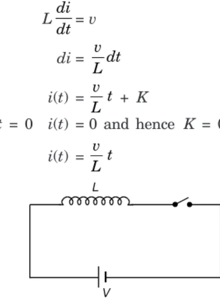
The differential equations describing the circuit in Fig. 1.3 when the switch is closed is Ldi dt=v or di= v Ldt i(t) = v L t + K At t = 0 i(t) = 0 and hence K = 0 and i(t) = v L t ...(1.18)
Fig. 1.3 An inductor switched into a d.c. source.
Even though under steady state condition the current through the inductor is theoreti-cally infinite but at t = 0+ the current is zero and the increase in current is gradual with time.
Capacitance
If a charge q is placed in space, this gives rise to an electric field. Again this field is not visible but its presence can be felt by bringing another charge in the vicinity of this charge. It is found that the charge experiences a force of attraction if it is of opposite polarity to that of q and vice versa. Also, if there are two metallic parallel plates separated by some distance d as shown in Fig. 1.4 and if one of the plates is charged with q+ charges, the other plate is charged with q– charges by induction and an electric field is set up between the plates and the two plates experience a force between each other. The force per unit charge is defined as the electric field strength. Now D =q
A where D is the field flux density and A is the area of plates. Also D = ∈ E where E is the electric field intensity.
Fig. 1.4 Electric field across plates of parallel capacitor.
Therefore E = q A
V d
∈ = where V is the voltage across the plates when the charge on the plate is q.
Therefore q
V =C = ∈ A
Here C is known as capacitance between the parallel plates separated by a distance d. So, capacitance depends upon the geometry of the conductors and ∈. If q is measured in coulombs and V in volts, C is measured in Farads. If q0 is the initial charge on the plates of the capacitor and while charging if the charge increases linearly with time, the charge at any instant is given as
q =q0 + Kt Hence, i = dq dt = K or q =q0 +
z
ti dt 0 ...(1.20) Also we know that q =C VAssuming C to be constant, it is seen that, an instantaneous change in q would mean an instantaneous change in voltage V. But from the integral equation for charge q, it is found that for finite value of i, the charge can’t change at t = 0+ and it remains q
0. Therefore, the voltage across a capacitor can’t change instantaneously.
Let us take up a few examples to illustrate the application of some of the relations obtained in the previous discussions.
Example 1.1: The current wave form in a series circuit of 500 Ω resistance and a 500 mH inductor is given in Fig. E1.1 (a). Determine the voltage wave form in the resistor, in the inductor and the total voltage.
Solution: Since the voltage drop across resistance = iR, the shape of the voltage is exactly same as that of the current and the magnitute
= 20 × 10–3 × 500 = 10 volt.
The voltage across the inductor
From 0 to 2 m sec, the change in current di is zero hence di
dt = 0. Hence the voltage across inductor from 0–2 m sec is zero volt.
From 2 to 3 m sec over 1 m sec, the change in current is 20 mA
i.e. = 20 10 1 10 3 3 × × − − = 20 A/sec Hence voltage L di dt = 500 × 10–3 × 20 = 10 volt.
From 3 m sec onwards since the change in current is zero. Hence voltage across inductor is zero. Therefore, the total voltage is the sum of two voltages vR + vL.
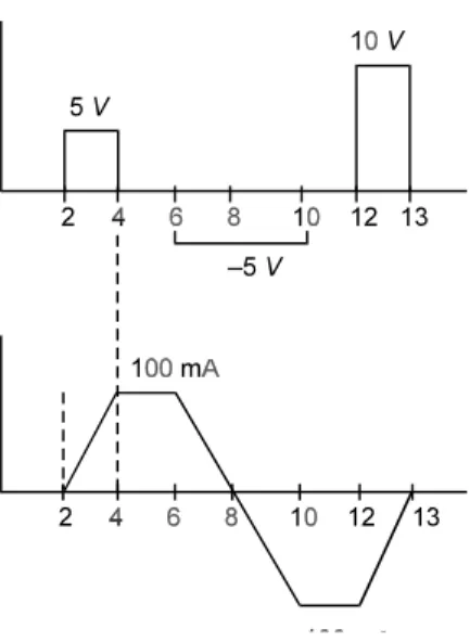
Example 1.2: Suppose if the voltage across an inductor is given, it is required to find out the current wave form through the inductor. Fig. E1.2 (a) shows voltage wave form across an inductor of 0.1 H.
Determine the current wave form:
Fig. E1.2 (a) Voltage wave from, (b) Current wave form.
Solution: In an inductor current i is given i = 1
L
z
v dt From 0 to 2 m sec v = 0. Therefore i = 0 From 2 to 4 m sec i = 1 0 1 5 10 5 2 100 4 2 4 .z
dt= t = mAFrom 4 to 6 m sec, v = 0 since there is no change in the current it continues to be same i.e. 100 mA From 6 to 10 m sec. i = 1 0 1 6 5 200 10 .
z
b g
− dt= − mAIt decreases linearly between 6 to 10 m sec. Hence the current at 10 m sec. is –200 + 100 = –100 mA
From 10 to 12 m sec. Since voltage is zero there is no change in current and it is –100 mA, from 12 to 13 m sec, the voltage is 10 volts. Hence current increases linearly by an amount
1 0 11210
13
.
z
dt = 100 mABeyond 13 m sec the current is zero.
Let us next consider application of non-sinuoidal voltages and currents in a capacitive circuit.
Example 1.3: Consider the application of a voltage wave form shown in Fig. E1.3 (a) to a 0.2 µF capacitor.
Determine the current wave form.
(a) Voltage. (b) Current wave form.
Fig. E1.3
Solution: Since current in a capacitor is given by i =C dv
dt From 0 to 2 m sec dv = 0 hence 0
2 = 0 Hence the current in this period is zero.
From 2 to 3 m sec the voltage increases linearly from 0 to 10 volts in 1 m sec. Hence v =kt, k = 10 1 10× −3 = 10 × 103 v/sec or 10 V/m sec i =C dv dt = 0.2 × 10 –6 × k = 0.2 × 10–6× 10 × 103 = 2 mA
Beyond 3 m sec since v is constant dv dt =0
Hence i = 0
The variation of current is shown in Fig. E1.3(b) 1.2.1 SINGLE-PHASE CIRCUIT
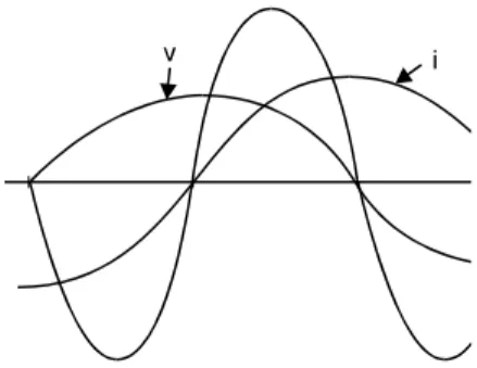
Let us consider an inductive circuit and let the instantaneous voltage be
v =Vm sin ωt ...(1.21)
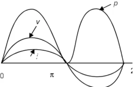
Then the current will be i = Im sin (ωt – φ) where φ is the angle by which the current lags the voltage (Fig. 1.5)
The instantaneous power is given by
p =vi = Vm sin ωt . Im sin (ωt – φ) =VmIm sin ωt sin (ωt – φ)
= V Im m t
2 cosf-cos
b
2w - fg
...(1.22)The value ‘p’ is positive when both v and i are either positive or negative and repre-sents the rate at which the energy is being consumed by the load. In this case the current flows in the direction of voltage drop. On the other hand power is negative when the current flows in the direction of voltage rise which means that the energy is being transferred from the load into the network to which it is connected. If the circuit is purely reactive the voltage and current will be 90º out of phase and hence the power will have equal positive and negative half cycles and the average value will be zero. From equation (1.22) the power pulsates around the average power at double the supply frequency.
Equation (1.22) can be rewritten as
p = VI cos φ (1 – cos 2 ωt) – VI sin φ sin 2 ωt ...(1.23)
Fig. 1.5 Voltage, current and power in single phase circuit.
Fig. 1.6 Active, reactive and total power in a single phase circuit.
(i) The component P marked Ipulsates around the same average power VI cos φ but never goes negative as the factor (1 – cos 2ωt) can at the most become zero but it will never go negative. We define this average power as the real power P which physically means the useful power being consumed.
(ii) The component marked II contains the term sin φ which is negative for capacitive circuit and is positive for inductive circuit. This component pulsates and has zero as its average value. This component is known as reactive power as it travels back and forth on the line without doing any useful work.
Equation (1.23) is rewritten as
p = P (1 – cos 2 ωt) – Q sin 2 ωt ...(1.24) Both P and Q have the same dimensions of watts but to emphasise the fact that Q represents a nonactive power, it is measured in terms of voltamperes reactive i.e. V Ar.
The term Q requires more attention because of the interesting property of sin φ which is –ve for capacitive circuits and is +ve for inductive circuits. This means a capacitor is a generator of positive reactive V Ar, a concept which is usually adopted by power system engineers. So it is better to consider a capacitor supplying a lagging current rather than taking a leading current (Fig. 1.7).
Fig. 1.7 V-I relations in a capacitor.
Consider a circuit in which an inductive load is shunted by a capacitor. If Q is the total reactive power requirement of the load and Q′ is the reactive power that the capacitor can generate, the net reactive power to be transmitted over the line will be (Q – Q′). This is the basic concept of synchronous phase modifiers for controlling the voltage of the system. The phase modifier controls the flow of reactive power by suitable excitation and hence the
voltage is controlled. The phase modifier is basically a synchronous machine working as a capacitor when overexcited and as an inductor when underexcited.
It is interesting to consider the case when a capacitor and an inductor of the same reactive power requirement are connected in parallel (Fig 1.8).
Fig. 1.8 Power flow in L-C circuit.
The currents IL and ICare equal in magnitude and, therefore, the power requirement is same. The line power will, therefore, be zero. Physically this means that the energy travels back and forth between the capacitor and the inductor. In one half cycle at a particular moment the capacitor is fully charged and the coil has no energy stored. Half a voltage cycle later the coil stores maximum energy and the capacitor is fully discharged.
Consider the case when the circuit is purely resistive when φ = 0 P =V I (1 – cos 2 ωt)
=V I – V I cos 2 ωt ...(1.25) which means, the average value of power in a purely resistive circuit consists of two components, one a constant value VI and superimposed over this is a sinusoidally varying with double the supply frequency and its average value is zero. Therefore, the net average power P = VI. The wave form is shown in Fig. 1.9.
Fig. 1.9 p, v and i wave form in a resistor.
Next we consider a purely inductive circuit when φ = 90º The power equation becomes
p =V I cos φ (1 – cos 2 ωt) – VI sin φ sin 2 ωt
=–V I sin 2 ωt ...(1.26)
This means the average power is zero.
Fig. 1.10 shows that there are four loops in the wave form for the instantaneous power. A positive loop shows that power is drawn from the source and negative loop shows that power is fed back to the source. The peak value of each loop is V I. Thus power or energy is taken from the source for a quarter cycle and then it is returned back to the source over
the next quarter cycle. The statement that the energy absorbed from the source is later restored to the source requires that the energy is stored and is not used up as heat or as mechanical energy. This concept implies that the 90º voltage current phase relation-ship must be for either an inductor or a capacitor since these are the two basic electrical elements that are capable of storing energy.
Fig. 1.10 Power relations when i lags v by 90°.
An inductor is a device capable of storing energy in the form of moving charge or in the form of a magnetic field. A capacitor is a device capable of storing energy in the form of separated charge or in the form of electric field.
The following example illustrates the relationship between the reactive power and the electric field energy stored by the capacitor. Consider an RC circuit (Fig. 1.11).
Fig. 1.11 Relationship between electric field energy and reactive power.
From Fig. 1.11 I = V R C V C R C 2 +(1ω )2 = 2 2 2 +1 ω ω ...(1.27)
and if voltage is taken as reference i.e. v = Vm sin ωt the current i =Im sin (ωt + φ) ∴ i = V C R C t mω ω ω φ 2 2 2 +1 ⋅sin ( + ) ...(1.28) where sin φ = I C I R I C R C / ( / ) ω ω ω 2 2 2 2 2 2 1 + = + ...(1.29)
Now reactive power Q = V I sin φ ...(1.30)
Substituting for I and sin φ, we have
Q =V V C R C R C ⋅ + ⋅ + ω ω ω 2 2 2 1 2 2 2 1 1 ...(1.31)
∴ Reactive power = V C
R C
2 2 2 2ω ω +1
Now this can be related with the electric energy stored by the capacitor. The energy stored by the capacitor,
W = 1 2 2 Cv ...(1.32) Now v = 1 1 1 2 2 2 C idt C V C R C m = + ⋅
z
ωω cos ( = V t R C mcos (ω φ) ω + + 2 2 2 1 ...(1.33) ∴ W = 12 1 2 2 2 2 2 2 2 C V t R C V R m ◊ + + = cos (w f) cos w w ...(1.34) dW dt = V R C t 2 2 2 2ω +1⋅2cos (ω +φ) sin (⋅ = V C R C t 2 2 2 2ω ω +1⋅sin (2 ω +φ) =Q sin 2 (ωt + φ) ...(1.35)From this it is clear that the rate of change of electric field energy is a harmonically varying quantity with a frequency double the supply frequency and has a peak value equal to Q.
In an R-L circuit the magnetic field energy and reactive power in a coil are similarly related.
1.2.2 The 3-phase Circuit
Assuming that the system is balanced which means that the three-phase voltages and currents are balanced. These quantities can be expressed mathematically as follows:
Va =Vm sin ωt Vb = Vm sin (ωt – 120º) Vc =Vm sin (ωt + 120º) ...(1.36) ia =Im sin (ωt – φ) ib =Im sin (ωt – φ – 120º) ic =Im sin (ωt – φ + 120º)
The total power in the circuit equals the sum of the individual powers in each phase. p =Vaia + Vbib + Vcic
= Vm sin ωt Im sin (ωt – φ) + Vm sin (ωt – 120º) Im sin (ωt – 120 – φ) + VmIm sin (ωt + 120º) sin (ωt + 120º – φ) = V I[2 sin ωt sin (ωt – φ) + 2 sin (ωt – 120º) sin (ωt – 120º – φ)
=V I[cos φ – cos (2 ωt – φ) + cos φ – cos (2 ωt – 240º – φ) + cos φ – cos (2 ωt + 240º – φ)
=3 V I cos φ ...(1.37)
This shows that the total instantaneous 3-phase power is constant and is equal to three times the real power per phase i.e. p = 3P, where P is the power per phase.
In case of single phase circuits we noted that the instantaneous power expression contained both the real and reactive power expression but here in case of 3-phase we find that the instantaneous power is constant. This does not mean that the reactive power is of no importance in a 3-phase system.
For a 3-phase system the sum of three currents at any instant is zero, this does not mean that the current in each phase is zero. Similarly, even though the sum of reactive power instantaneously in 3-phase system is zero but in each phase it does exist and is equal to V I sin φ and, therefore, for 3-φ the reactive power is equal to Q3φ = 3V I sin φ = 3Q, where Q is the reactive power in each phase. It is to be noted here that the term Q3φ makes as little physical sense as would the concept of three phase currents I3φ = 3I. Nevertheless the reactive power in a 3-phase system is expressed as Q3φ. This is done to maintain symmetry between the active and reactive powers.
1.2.3 Complex Power
Consider a single phase network and let
V = |V|ejα and I = |I|ejβ ...(1.38)
where α and β are the angles that V and I subtend with respect to some reference axis. We calculate the real and reactive power by finding the product of V with the conjugate of I i.e.
S =V I* = |V|ejα |I|e–jβ = |V| |I|ej(α – β)
= |V| |I| cos (α – β) + j |V| |I| sin (α – β) ...(1.39) Here the angle (α – β) is the phase difference between the phasor V and I and is normally denoted by φ
∴ S = |V| |I| cos φ + j |V| |I| sin φ
=P + jQ ...(1.40)
P =Re [V I*] and Q = I
m [V I*] ...(1.41)
The quantity S is called the complex power. The magnitude of S = P2 +Q2 is termed as the apparent power and its units are volt-amperes and the larger units are kVA or MVA. The practical significance of apparent power is as a rating unit of generators and transform-ers, as the apparent power rating is a direct indication of heating of machine which deter-mines the rating of the machines. It is to be noted that Q is positive when (α – β) is positive i.e. when V leads I i.e. the load is inductive and Q is –ve when V lags I i.e. the load is capacitive. This agrees with the normal convention adopted in Circuit Theory i.e. taking Q due to an inductive load as +ve and Q due to a capacitive load as negative. Therefore, to obtain proper sign for reactive power it is necessary to find out V I* rather than V*I which would reverse the sign for Q as
V*I = |V|e–jα |I|ejβ = |V| |I|e–j(α – β)
= |V| |I| cos (α – β) – j |V| |I| sin (α – β) = |V| |I| cos φ – j |V| |I| sin φ
=P – jQ ...(1.42) P =Re [V * I] and Q = – I
m [V * I] ...(1.43) 1.3 NETWORK CLASSIFICATION
Electric networks can be classified mainly in two ways. The first one is based on the kind of elements in the network e.g. time-invariant or nonlinear or time variant etc. The second one is based on excitation and response i.e. for a given excitation the response decides the type of network.
Here we shall study classification based on the second approach. 1.3.1 Linearity
Suppose the network to be classified is under relaxed condition i.e. the initial condition is zero and an excitation v1(t) is applied for which response is c1(t) and for excitation v2 (t) the response is c2 (t). Then the network is classified as linear if for excitation v1 (t) + v2 (t) the response is c1 (t) + c2 (t). This shows that a linear network follows superposition principle. 1.3.2 Passivity
Some networks have the property of absorbing/dissipating or storing energy. These are able to return the energy previously stored to the external network. However, this energy returned is never more than the energy stored. Such networks are known as passive networks.
Let network N be connected to a source S. Suppose the network is initially relaxed. If v(t) is the voltage of the source and i(t) is the resulting current into the network N, the average power delivered into the network is p(t) = v(t) i(t) and the energy delivered w(t) over time t is given by w(t) = v t i t dt t ( ) ( ) −∞
z
...(1.44) This energy will always be non-negative for a passive network i.e. over time t there will always be some energy delivered to the network or at least there will not be any energy when the network would have returned all the energy back to the source or it would have stored some energy. It will never be a situation for a passive network when it would supply more energy what it had drawn previously. Mathematically for a passive network.w(t) = tv t i t dt( ) ( ) ≥ −∞
z
0 ...(1.45)
However, if the network has some initial energy stored equal to w(t0) before it is switched on to a supply at t = t0, then for a passive network energy delivered to the network from the source should satisfy the inequality at any time t
w(t) = v t i t dt w t t
( ) ( ) + ( )≥ −∞
z
A circuit which does not satisfy this condition is known as active circuit. That is for an active circuit v t i t dt t ( ) ( ) < −∞
z
0 ...(1.47) 1.3.3 LumpedMany devices in electric system are distributed in space e.g. transmission lines, the wind-ings of transformers or that of the generators, are distributed in a way. Whenever these devices are energized, the effect is not experienced by the line length or winding lengths instantly because of finite velocity of electric signals. However, if we are interested in steady state and terminal quantities, it is sufficient to assume the parameters to be lumped rather than distributed. Sometimes when we are interested in the intermediate values and point to point variation of electric signals, we talk true nature of these devices i.e. the distributed nature. Otherwise, we assume the parameters to be lumped. In this book we treat these parameters as lumped unless it is specified otherwise.
1.3.4 Bilateral
The elements to be considered for electric network are assumed to be bilateral which means the voltage and current relations are same irrespective of direction of flow of current e.g. resistance, inductance, etc. However, for unilateral elements the voltage and current are different for two possible direction of flow of currents e.g. diodes.
1.3.5 Time Invariance
A network is said to be time-invariant when there is some response to a certain excitation irrespective of time of application of excitation. Suppose for certain excitation v1 (t) the response is c1 (t), if now the excitation is v (t + t0) the response would be c (t + t0). Here the values of the parameters are assumed to be constant at all times and do not change with time.
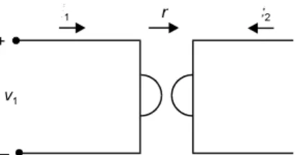
1.3.6 Reciprocity
A network is said to possess the property of reciprocity when excitation and response terminals could be interchanged. Consider network N with terminals 1 and 2 as shown in Fig. 1.12.
(a) (b)
Fig. 1.12 Networks to describe reciprocity.
Say if v1 is excitation and i2 response as in Fig. 1.12 (a) and if v2 is excitation then i1 is the response as in Fig. 1.12 (b) The network is reciprocal if for v1 = v2, i1 = i2. A transmission line is a reciprocal network. The network which does not satisfy the condition
is a non-reciprocal network. R, L, C, are in general linear, passive, bilateral, time invariant and lumped elements. Since L and C can store energy in the form of electro-magnetic and electro-static fields respectively their representation needs special mention. In general volt-age across capacitor is given by
v(t) = 1
C
z
i t dt v o( ) + ( ) ...(1.48) where v(o) indicates the voltage due to initial charge. The capacitor which has initial voltage v(o) can be represented as shown in Fig. 1.13(a).(a) (b)
Fig. 1.13 Initial condition for a capacitor and inductor.
Similarly if an inductor initially has a current i(o) the current at anytime t is given by i(t) = 1
L
z
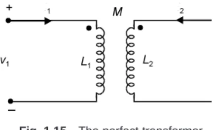
v t dt i o( ) + ( ) ...(1.49) Therefore, i(o) could be considered as a d.c. current source in parallel with an initially relaxed (initial condition zero) inductor as shown in Fig 1.13(b).1.4 THE TRANSFORMER
It is a two port network. An ideal transformer shown in Fig. 1.14 is described by the following equations:
(a) (b)
Fig. 1.14 The ideal transformer.
For Fig. 1.14 (a)
v1 =n v2 and i2 = –n i1 ...(1.50) If the direction of i2 is reversed as what is given in Fig. 1.14 (b), i2 = ni1
In matrix notation v i21
L
NM
O
QP
= 0 0 n n −L
NM
O
QP
i v12L
NM
O
QP
...(1.50)It can be seen that an ideal transformer is characterized by a single parameter n known as turns ratio. The v-i relationships indicate idealized relations expressing Faraday’s law (v1 = n v2) and Ampere’s law (i2 = –n i1). Another characteristic of an ideal transformer is that a resistance R connected on to secondary side is reflected as n2R when referred to the primary side.
Also it can be seen easily that the total energy input to the ideal transformer is zero. Total energy input = (v ii i v i dt)
t + −∞
z
2 2 = n v i n v i dt t 2F
HG
− 2I
KJ
+ 2 2R
S
T
U
V
W
−∞z
= (− + ) −∞z
v i v i dt t 2 2 2 2 = 0 ...(1.51)This shows that an ideal transformer is a passive device, it transmits energy, it neither stores nor dissipates the energy. It can be summarized that an ideal transformer is
(i) an abstract concept;
(ii) characterized by a single parameter n, the turns ratio;
(iii) the voltage and current are idealized relations derived out of Faraday’s law and Ampere’s law respectively;
(iv) One where a resistance R connected to secondary side is reflected as n2R when referred to primary side; and
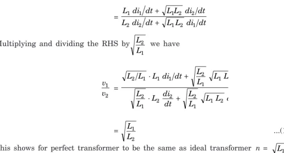
(v) a passive device. 1.4.1 The Perfect Transformer
A less abstract model of a real life transformer is shown in Fig. 1.15.
Fig. 1.15 The perfect transformer.
The v-i relations for the perfect transformer are given as v1 =L di dt M di dt 1 1 + 2 ...(1.52) v2 =L di dt M didt 2 2 + 1 ...(1.53)
Thus this is characterized by three parameters L1, L2 and M the two self inductances and one mutual inductance in contrast to ideal transformer which is characterized by a single parameter n. The total energy delivered to the transformer is
= t(v i1 1 +v i dt2 2) −∞
z
= L di dt M di dt i dt L t t 1 1 + 2 1
F
HG
I
KJ
+F
HG
−∞z
−∞z
= L i di M i di i di i i i 1 1 1 0 2 1 1 2 0 1 1 2 + +z
z
( , = 1 2 1 2 1 12 1 2 2 22 L i + M i i + L i ...(1.54)For perfect transformer to be passive, the energy stored should be non-negative i.e. L i1 12 M i i L i
1 2 2 22
2 0
+ + ≥ ...(1.55)
To prove that it is non-negative, we prove that the minimum of this is non-negative and hence the expression will be non-negative for all other values.
Let i2 = –xi1 where x is a real positive number. The above expression reduces to
f (x) =L1 i12 –2 Mx i 12 +L2 x2 i12 df x dx ( ) = – 2M i12 + 2 x L 2 i12 = 0 or x = M L2 Substituting value of x in f (x) we have
f (x) = L M L M L 1 2 2 2 2 2 0 − +
F
HG
I
KJ
≥ or L1L2 – M2 ≥0 or M2 ≤L 1L2 or L LM 2 1 2 ≤1 Let K2 = M L L 2 1 2 or K = M L L1 2 Since this inequality is true, the inequality (1.55) is also true.Here K is known as co-efficient of coupling and its maximum value is unity when this transformer is known as a perfect or perfectly coupled transformer. It can be seen that a perfect transformer is not same as ideal transformer. To establish the difference we know that in case of ideal transformer v
v12 =n In case of perfect transformer
v v12 = L di dt M di dt L di dt M di dt12 12 21 + +
= L di dt L L di dt L di dt L L di dt 1 1 1 2 2 2 2 1 2 1 + + Multiplying and dividing the RHS by L
L21 we have v v12 = L L L di dt L L L L L L L didt L L L L d 2 1 1 1 2 1 1 2 1 2 2 2 1 1 2 ⋅ + ⋅ + = L L12 ...(1.58)
This shows for perfect transformer to be the same as ideal transformer n = L L1 2. Again, using current relations it can be shown that if in a perfect transformer i1 and i2→ ∞ but such that their ratio remains constant, the result will be an ideal transformer. Fig. 1.16 shows relation between a perfect and an ideal transformer.
Fig 1.16 A perfect transformer and an ideal transformer relations.
1.5 THE GYRATOR
A gyrator is another two-port terminal device shown in Fig. 1.17
(a) (b)
Fig. 1.17 A Gyrator.
For Fig. 1.17 (a) v r i v r i v v o r r o i i 1 2 2 1 1 2 1 2 = -=
L
N
M
O
Q
P
=L
-N
M
O
Q
P
L
N
M
O
Q
P
or ...(1.59) For Fig. 1.17 (b) v r i v r i v v o r r o i i 1 2 2 1 1 2 1 2 = = −L
N
M
O
Q
P
=L
−N
M
O
Q
P
L
N
M
O
Q
P
or ...(1.60)Here r is known as gyration resistance. The direction of arrow associated with r gives the direction of gyration.
The gyrator is a hypothetical device which is introduced to account for physical situ-ations where the reciprocity condition does not hold. It can be shown that gyrator is not a reciprocal device, it is anti-reciprocal.
The total energy input to the gyrator
E(t) = (v i v i dt) t 1 1 + 2 2 −∞
z
= (− ) + −∞z
ri i ri i dt t 2 1 1 2l
q
= 0 ...(1.61)Hence it is a passive device. Suppose the gyrator is terminated through a resistance R, it’s equivalent on the input side is given by
v1 = –ri2 = – r
HG
F
−RvI
KJ
=r r i = R r G i2 1 2
1
( ) ...(1.62) Thus, the equivalent resistance at the input terminals equals r2 times the conductance terminating at the output terminals. The gyrator, therefore, has the property of inverting. A very interesting case is found when the gyrator is terminated through an inductor or a capacitor. Say it is terminated through a capacitor. The equivalent of this when referred to input side is obtained as follows.
Fig. 1.18 Gyrator terminated through a capacitor.
v1 = − = −
F
−HG
I
KJ
= ri r C dv dt rC d dt r 2 ( ) 2 ( = r C di dt di dt 2 1 =Leq 1 ...(1.63)This shows that through inversion a r2 times capacitor is equivalent to an inductor and it can be shown that an inductor is inverted as a capacitor.
It is found that in electronic circuits it is difficult to have inductors of suitable values. These can be simulated through the use of a gyrator terminated through a suitable capacitor. Fig. 1.19 shows a general representation of a gyrator and its v-i relations are given as
Fig. 1.19 A general gyrator.
V1 = –I2 r1 and V2 = I1 r2
The arrow here indicates that the device has a forward transmission path and this has no backward transmission.
If r1 = r2 = r it is known as an ideal gyrator and it is a passive device. However if r1≠ r2 it is an active device as power can be made negative as shown here. Power delivered to the gyrator is
V1 I1 + V2 I2 = (r2 – r1) I1 I2 ...(1.64) Therefore, with this it is an active device. The input impedance of the gyrator is
Zin = V I I r V r I V r r 1 1 2 1 2 2 2 2 1 2 = − = −
F
HG
I
KJ
= r r ZL 1 2 ...(1.65)1.6 THE NEGATIVE CONVERTER
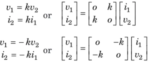
The next two pair terminal device is the negative convertor which is characterized by the following v-i relations
v kv i12 ki12 = = or v i o k k o i v 1 2 1 2
L
NM
O
QP
=L
NM
O
QP
L
NM
O
QP
or vi1 kvki2 2 1 = − = − or v i o k k o i v 1 2 1 2L
NM
O
QP
= − −L
NM
O
QP
L
NM
O
QP
...(1.66)Fig. 1.20 shows a general representation of negative converter, It is characterised by a single parameter k known as conversion ratio.
It can be seen from the first set of equations that when i1 is in the reference direction i2 is also in the reference direction and hence the current is said to be inverted in going through the negative converter. However, the voltage is not inverted. Therefore, the first set of equations characterise a current negative converter. However the second set of
equations show that the voltage is inverted but the current is not and therefore, these equations characterise a voltage negative converter.
(a) (b)
Fig. 1.20 Negative converters (a) Current negative converter (b) Voltage negative converter.
Let us study the behaviour of these devices when these are terminated through a passive element. Suppose these are terminated through an inductor L. Then the voltage v2 = –L di2/dt Inserting the value of v2 in the v-i relations of the two negative converters we have
v1 = ± = ±
F
H
-I
K
= ±L
-N
M
k v k L di dt k Lk 2 2 = −L k di dt 2 1 ...(1.67)Here ± signs indicate the application to INC and VNC respectively.
Thus at the input terminals, the equivalent inductance is – k2L i.e. negative of the k2L. Hence the device is termed as negative converter.
Similar conclusions can be drawn by terminating the device with R or C. 1.7 INDEPENDENT SOURCES
So far we have considered passive elements when interconnected, form a network. A network without an active source is meaningless. Mainly there are two types of sources (i) Voltage source (ii) Current source. Again these are classified as ideal or independent and dependent sources.
1.7.1 Ideal Voltage Source
An ideal voltage source is a two terminal device whose terminal voltage is independent of the current drawn by the network connected to its terminals. Both the magnitude and wave form of voltage remain unaffected. This means an ideal voltage source should have zero internal resistance. It is to be noted that short circuit at the terminals of an ideal voltage source makes no sense as this would impose two conflicting requirement. Fig. 1.21 shows the symbols and reference conventions for such a source and the voltage current characteristic.
(i) (ii) (iii)
When the voltage generated does not change with time, it is represented by a battery as shown in Fig. (iii) otherwise for all the cases by Fig. (i)
However, in actual practice, there is no voltage source which does not have internal resistance, however small it could be and, therefore, an actual voltage source is always associated with an internal resistance as shown in Fig. 1.22.
(a) (b)
Fig. 1.22 (a) Voltage source (b) v-i characteristic.
Therefore, the terminal voltage decreases as the current drawn by the external net-work increases and the voltage current relation is as shown in Fig. 1.22(b).
1.7.2 Ideal Current Source
It is a two terminal device which delivers a constant current to the network connected across its terminals irrespective of the elements of the network i.e. the current is independent of the voltage across its terminals. Here again it makes no sense to consider open circuiting of the terminals of a current source as this again imposes two conflicting requirements at the termi-nals. The voltage at the terminals will be determined by the network connected across its terminals. Fig. 1.23 shows the symbol and reference convention for the current source and also the v-i characteristic of such a source.
(a) (b)
Fig. 1.23 (a) Ideal current source (b) i-v characteristic.
Certain devices may be represented by the model shown in Fig. 1.24 wherein a resistor is connected across the current source. The corresponding variation of terminal current with voltage at the terminals is shown in Fig. 1.23(b) Such devices as transistors and photo electric cells are examples of current sources.
(a) (b)
Fig. 1.24 (i) Current source (ii) v-i charisteristic.
It can be seen that the voltage and current sources are dual in the sense that the roles for current and voltage are interchanged in the two sources.
1.8 THE DEPENDENT OR CONTROLLED SOURCES
A controlled voltage/current source is one whose terminal voltage/current is a function of some other voltage or current. These devices have two pairs of terminals, one pair corre-sponds to the controlling quantity and the other the controlled quantity. Here the controlled voltage/current is directly proportional to the controlling voltage or current.
There are controlled sources where the voltage/current is proportional to derivative of some other voltage or current. Here controlled source will not be considered for the present. 1.9 SOURCE TRANSFORMATION
In order to make the network manipulations direct and simple, following aspect would be considered:
(i) Transformation of voltage source into a current source and vice versa. (ii) Shifting the positions of the sources in the network.
In doing this, it is to be remembered that the terminal conditions i.e.vandiof these sources remain unchanged with respect to the external network to be connected to these sources.
Suppose there are two voltage sources in series as shown in Fig. 1.25, the equivalent will be one source with voltage (v1 + v2).
However, it is to be noted that two voltage sources can’t be connected in parallel unless these are identical in magnitude and wave shape and similarly two current sources can’t be connected in series unless these are identical. We know that two generators can’t be
(a) (b)
Fig. 1.25 (a) Two voltage sources in series, (b) Two current sources in parallel.
connected in parallel unless their voltages are exactly identical otherwise, this results in a short circuit and the generators get damaged.
Fig. 1.26 (a) shows a resistance R connected across a voltage source v and Fig. 1.26 (b) shows a resistance R in series with a current source when an external network is connected across the terminals of these source circuits. From computation point of view, the resistor across the voltage source and/or a resistor in series with the current source can be ignored as shown in Fig. 1.26 (a) and (b) respectively.
(a) (b)
In network analysis, sometimes it may be more convenient to transform a voltage source into a current source and vice versa from computation point of view. To this, the basic criterion is that the terminal conditions (v and i) of the two networks, the source and the external network must remain same before and after the transformation.
Let us transform a voltage source into a current source. Refer to Fig 1.27.
v t( ) v t1( ) ≡ E xt.
C kt 1s
R I
Fig. 1.27 Voltage to current source transformation.
v =v1 + I R ...(1.68) or I = v R v R − 1 ...(1.69)
Equation (1.68) represents Fig. 1.27 (a) whereas equation (1.69) which has been derived from equation (1.68) represents Fig. 1.27 (b) and hence Fig. 1.27 (a) and (b) are equivalent of each other.
Similarly if the series element is an inductor or a capacitor with the voltage source Fig. 1.28 (a) and (b), the equivalent current source is given by the circuit as shown in Fig. 1.28.
(a) + v C v1 i i s= C (b)
Fig. 1.28 (a) Inductor in series, (b) Capacitor in series.
Fig. 1.29 Current to voltage source transformation. is = i v R + 1 ...(1.70) or is R =i R + v1 or v1 =vs – i R ...(1.71)
If an inductor is connected across a current source (Fig. 1.30)
Fig. 1.30 Inductor across current source.
is = i
L v dt
+ 1
z
1 ...(1.72)or L is = Li+
z
v dt1Differentiating the equation gives L di dts =L di dt +v1 or v1 =L di dt L di dt s − ...(1.73)
Similarly an equivalent voltage source can be obtained when a current source is con-nected across a capacitor.
It is to be noted that a single passive element when connected in series with a voltage source or across a current source its equivalent current or voltage source can be obtained by the method explained above. However for more than one passive elements when consid-ered, above method can’t be used, as the determination of the source equivalent involves the solutions of the differential equation.
In many situations a voltage source may not be associated with a series passive element, and a current source with a parallel passive element. Here, before transformation could be carried out, it is necessary to shift the source within the network. A voltage source is shifted from one branch to the network by the process known as “push the voltage source through the node” with a new identical source appearing in every branch connected to the node such that it does not affect the current distribution in the network as shown in Fig 1.31.
Fig. 1.31 Voltage source shift in a network.
It is to be noted that whereas current distribution remains unaffected, the voltage dis-tribution in the network is changed since node ‘o’ is at the same potential as ‘d’ after the shift. In order to shift current sources, it is required to maintain the same currents at all nodes of the network by adding and then subtracting the same current quantity as shown in Fig. 1.32.
Fig. 1.32 Shifting of current sources.
In the current source shifting process, the voltages are not changed by the transfor-mation even though the currents in the active source branches are changed.
While drawing graph from a network, the source transformation makes following suggestions:
(i) Elements in parallel with voltage source or in series with a current source can be eliminated from the graph.
(ii) When voltage source is shifted and hence pushed through the node, the voltage source may be short-circuited and the current source may be open circuited and so eliminated from the graph which represents the network.
While preparing a network before analysis following thumb rules are to be followed for convenience. If the network is to be analysed on nodal basis, the network should contain current sources and if it is to be analysed on loop basis, the network should contain voltage sources. However, if it is to be analysed based on state variable approach, the network may contain both kinds of sources.
1.10 DOT CONVENTION FOR COUPLED CIRCUITS
Suppose a time varying voltage source is connected across the primary of the trans-former and at any given instant the voltage source has the polarity shown and current i (t) is in the direction shown by the arrow and is increasing with time entering the dotted terminal, this current induces a voltage in the secondary which is positive at the dotted
Fig. 1.33 A circuit for dot convention.
terminal. Conversely if the current in the primary is increasing and is leaving the dotted terminal this will induce the voltage polarity in the secondary such that the undotted end will become positive and hence dotted terminals of both the windings will be negative simultaneously. The following experimental procedure can be used to establish dotted ends of the transformer windings. Mark a dot arbitrarily on one end of the primary winding and connect a d.c. source with positive terminal connected to the dotted end and the negative terminal to the undotted end of the winding through a switch. Connect a MC voltmeter across the secondary winding. The end of the secondary winding which goes positive momentarily on closing the switch on the primary side as measured by the voltmeter, is the terminal to be dotted.
If there are more than two windings, similar procedure can be followed for identifying relationship between each pair of windings. For each pair of winding different forms of dots (l v n ]) should be used to avoid any confusion.
Suppose we are required to write loop equations for a mutually coupled circuit shown in Fig 1.34. r1 r2 i2 v t( ) i1 M
Fig. 1.34 Coupled circuit.
For primary loop the drops are i1r1 +L di dt
1 1 + drop in primary loop due to current in secondary loop. The voltage induced in primary will be determined by the direction of i2 with respect to its dot in secondary loop. Since current is going away from the dot, the polarity of voltage on the primary side will be positive at the undotted terminal. Therefore, for current i1 it will be rise in voltage and the equation will be
i r L di
dt M
di dt
1 1 + 1 1 - 2 = v(t)
and for the secondary loop, similarly i2 r2 + L2di
dt M di
dt
The equivalent two loops are as shown in Fig. 1.35.
Fig. 1.35 Equivalent of Fig. 1.34.
Consider Fig. 1.36 which is a magnetically coupled network
Fig. 1.36 Magnetically coupled network.
The equivalent with dots is given in Fig. 1.37.
Fig. 1.37 Equivalent of Fig. 1.36.
Since all the three coils are mutually coupled, each coil will induce voltage in the other two coils, the magnitude will depend upon the current flowing through the coil and the polarity its relative direction of flow with respect to dot of the coil.
Voltage induced in coil 1
Due to coil 2, the current through coil 2 is (i2 – i3) entering the circular dot, therefore the voltage induced in coil 1 will be with positive polarity at the dot. Due to coil 3, since the current i3 is leaving the triangular dot, the polarity will be –ve at the corresponding dot in coil 1.
Voltage induced in coil 2
Due to coil 1, the current (i1 – i2) enters the dot, therefore positive polarity at the dot of coil 2.
Due to coil 3, the current i3 leaves the dot (square), the polarity +ve will be at the undotted terminal of coil 2.
Voltage induced in coil 3
Due to coil 1 the current entering the dot is (i1 – i2) hence the positive polarity at the dotted terminal of coil 3. Due to coil 2 current (i2 – i3) leaves the dot (square), the positive polarity will be at the undotted terminal. Hence the equivalent circuit given as follows:
Fig. 1.38 Equivalent of Fig. 1.36 with voltage sources.
The loop equations can be written as follows: Loop 1 Ri M d i i dt L d idt 1+ 12 (2- 3) + 1 (1 -Loop 2 M di dt L d i i dt M d 13 3 + 1 (2 − 1) − 12 + L d i −i + = dt M di dt 2 (2 3) 23 3 0 Loop 3 L d i i dt M di dt M d 2 (3− 2) − 23 3 − 21 + L di + − +
z
dt M d i i dt C 3 3 32 (2 3) 1The above example explains clearly how voltage sources (corresponding to induced voltages) are inserted in the coils which are magnetically coupled and the dots have been assigned.
When the two coils are to be interconnected it is important to know whether the mutual inductance M is aiding or opposing. However, it is known that the effect on each of the two coils must be the same. Refer to Fig. 1.39(a) where the mutual inductance is aiding their self inductances whereas in (b) it is opposing. If L1 and L2 are the self induc-tances of the two coils and M the mutual inductance, the total inductance say if is LA in case of Fig. 1.39(a) and LB that in Fig 1.39(b) then,
Fig. 1.39 (a) Two coils aid and (b) Oppose.
Fig. 1.40 The coils at right angles.
LA =L1 + L2 + 2M and LB =L1 + L2 – 2M
Therefore,
M = LA − LB
4
This method provides a very convenient way of determining the value of mutual inductance between the coils.
The co-efficient of coupling and the mutual inductance between the two coils shown in Fig 1.40 are both zero. Although the flux of one coil appears to pass through the other coil, it does not actually link the turns of the other coil.
Therefore, the linkages are zero and the value of M is zero. It is only when one coil is rotated with respect to other that a linking occurs.
Example 1.4: Determine the inductance of the individual winding and the equiva-lent inductance when mutual inductance is 8H.
Since the flux through the two coils opposes each other, the mutual inductance is substractive from each coil and hence
Fig. E1.4
L1 = 15 – 8 = 7H
Therefore equivalent inductance between the terminals L = L L L11 L22 7 8 15 3 73 + = = × . H
Example 1.5: Determine the inductance between the terminals for a three coil system shown below:
Fig. E1.5
From the Fig.
LA = 25 + 10 – 10 = 25H LB = 30 + 10 – 15 = 25H LC = 35 – 15 – 10 = 10H Therefore, 1 Leq = 1 25 1 25 1 10 2 2 5 50 + + = + + or Leq = 50 9 =5 55. H
For further analysis of coupled circuit see Appendix B.
A given network will always have a unique solution in terms of its nodal voltages and loop currents. It is, therefore, required to write down a set of linearly independent simul-taneous equations equal to the number of unknowns, and smaller the number of unknowns fewer the linear simultaneous equations and less time consuming will be the solution of these equations. It would be seen that sometimes it is more convenient to use nodal voltages as independent variables, sometimes loop currents as independent variables and yet some-times a suitable combination of both from the point of view of minimum independent variables required to describe the netowrk and hence the number of equations to seek solution of the network.
If ‘n’ is the number of nodes and ‘b’ the number of branches in a given network, the minimum number of independent nodal voltages (nodal analysis) minimum number of independent loop currents (loop analysis) to describe the network uniquely is given by (n – 1) or (b – n + 1) respectively. Therefore, from solution point of view, whichever is smaller of the two should be used for analysis of a given network. However, it may be mentioned here that there could be situations when it could be mandatory to use only a particular kind of variables (viz. nodal vollages) as we may not be interested in the other kind of variables (viz. loop currents).
Example 1.6: Fig. E1.6(a) shows a gyrator which is described by the equation v1 =i2r
(a) gyrator (b) its equivalent
Fig. E1.6
Determine the two element equivalent network shown in Fig. E1.6(b)
Solution: i2 = –v R C dv dt 2 − 2 Now v2 = –i1r or dv dt di dt r 2 = − 1 Hence i2 = v r1 = + i r R rC di dt 1 + 1 or v1 =i r R r C di dt 1 2 2 1 + Hence the two elements are Req = r
R 2
and Leq =r2C
Example 1.7: Two gyrators are connected in cascade. Derive the terminal relations for the network.
Fig. E1.7 v1 = –ir1 v = –i1r1 = i2 r2 v2 = –ir2 To eliminate v and i v2 = v r11 r2 = r r21v1 and i2 = −r r21i1
The relations show that two gyrators connected in cascade behave as an ideal trans-former with ratio as r
1.11 MAGNETIC CIRCUITS
Oersted in 1819 discovered that a current flowing in a straight conductor deflected the needle of a compass and it shows that the paths of magnetic force are concentric circle around the conductor. Similarly if a current is passed through circular (loop) conductor the magnetic flux are found to be concentric to the circular conductor and the magnetic flux density at the centre of the circular conductor is given by (loop)
B = µ2Ir
where B is the magnetic flux density in Wb/m2 or in Tesla, I the current flowing through the circular loop of the conductor and r the radius of the circular loop, µ the permeability of the material around which the loop is wound.
µ =µ0 = 4π × 10–7 H/m
if the coil is wound on a non-magnetic material or it is air cored and µ = µ0 µr
where µr is the relative permeability of the magnetic material. The magnetic flux density is related to magnetic field intensity through µ as given below.
B =µ0 µr H
where H is the magnetic field intensity and its units are Ampere turns per meter. µr has no units as it is a relative permeability, µ is permeability of the material and its units are Henry/m.
As far as analysis of magnetic circuits is concerned, it is analogous to electric circuits. The analogous quantities are listed below.
Electric Circuits Magnetic Circuits
e.m.f. (Volts) mmf (amp. Turns)
Current (Ampere) Flux (Webers) Resistance, ohm Reluctance, R
Conductance S Permeability
Henry/m Electric field intensity, E V/m Magnetic field
Intensity, H AT/m Electric flux density Magnetic flux density
D coulomb/m2 Wb/m2
Simple magnetic circuits can be analysed based on ohm’s law in Electric circuits. According to Ohm’s Law
V I =R
whee V is the e.m.f. I the current and R the resistance. Picking up analogous quantities in magnetic circuits from the relations given above we have
mmf
flux = Reluctance N I
φ = Reluctance where N is the number of turns in the circular coil.
Now φ = BA where A is the area of cross section of the core on which the coil is wound.
Now B =µ0 µr H
and H = N I
l where l is the length of the magnetic path. Hence reluctance R = N I N I l A r µ µ0 ⋅ = l A r µ µ0 AT/Wb
1.11.1 Series Magnetic Circuit
If there are one or more than one magnetic paths connected in series there could even be an air gap in the path of the same flux (same current in a series electric circuit), the net reluctance is the sum total of the individual magnetic paths.
1.11.2 Parallel Magnetic Circuits
Analogous to electric circuit, the magnetic circuit will be analysed using Kirchhoff’s laws as shown in Fig. 1.41.
Fig. 1.41 Analogous parallel electric circuits
Let us take a few examples to illustrate the application of what we have studied about the magnetic circuits.
Example 1.8: An iron ring of mean length 50 cms has an air gap of 1 mm and a winding of 200 turns. If the relative permeability of air is 300 when a current of 1 A flows through the coil, find the flux density.
Solution: