Progress of 2-micron Detectors for Application to Lidar Remote Sensing
M.N. Abedina, T.F. Refaatb, S. Ismaila, G. Kocha, and U.N. Singhaa
NASA Langley Research Center, Hampton, VA 23681
b
Old Dominion University, Norfolk, VA 23529
Abstract - AlGaAsSb/InGaAsSb
heterojunction phototransistors were developed at Astropower, Inc under Laser Risk Reduction Program (LRRP) for
operation in the 2-µm region. These
phototransistors were optimized for 2-µm detection and have high quantum efficiency
(>60%), high gain (>103) and low
noise-equivalent-power (<5x10-14 W/√Hz), while
operating at low bias voltage. One of these phototransistors was tested in lidar mode
using the 2-µm CO2 Differential Absorption
Lidar (DIAL) system currently under development under the Instrument Incubator Program (IIP) at NASA Langley. Lidar measurements included detecting atmospheric structures consisting of thin clouds in the mid-altitude and near-field boundary layer. These test results are very promising for the application of phototransistors for the two-micron lidar remote sensing. In addition, HgCdTe avalanche photodiodes (APD) acquired from Raytheon were used in atmospheric
testing at 2-µm. A discussion of these
measurements is also presented in this paper.
I. INTRODUCTION
Considerable interest exists in 2-micron detector, which can be used to detect temporal and spatial distribution of aerosols, clouds, CO2, O3, H2O, and CH4. Therefore, NASA
Langley detector group put a plan together to develop 2-micron detector, which was funded by NASA’s Earth Science Technology Office within the Laser Risk Reduction Program (LRRP). Improvements of detector
parameters, such as high quantum efficiency, high gain, and low noise-equivalent-power (NEP) were the required areas of interest. An antimonide (Sb)-based heterojunction phototransistor (HPT) showed promise to meet the detector requirements for applications to the active remote sensing systems. In addition, this detector operated without the excess noise factor and at lower operating bias voltages [1-3]. HPT has an internal gain mechanism that allows increasing the output signal and signal-to-noise ratio (SNR).
AlGaAsSb/InGaAsSb HPTs in the 1.0-to 2.3-µm wavelength range have been developed and fabricated at Astropower, Inc. in collaboration with NASA Langley Research Center (LaRC) using Liquid Phase Epitaxy (LPE) growth technique [2-7]. These HPTs have been characterized at NASA LaRC, and results including high quantum efficiency (>60%), high gain (>103), high detectivity (3.9x1011 cm.√Hz/W), and relatively low NEP (4.6x10⁻¹⁴ W/√Hz) have been obtained [2,4,6-7].
Based on the phototransistors’ performances, lidar tests have been carried out successfully at National Center for Atmospheric Research (NCAR), Boulder, Colorado, operating at 1.543 micron [8-10]. Recently, lidar tests have been undertaken at NASA LaRC to validate the phototransistor operation at 2-micron wavelength by integrating it into the 2-µm receiver system. These studies were supported by 2-µm CO2
Differential Absorption Lidar (DIAL) Instrument Incubator Program (IIP). The main focus of these tests was to acquire lidar backscatter signals through the phototransistor and HgCdTe APD (Raytheon Vision Systems)
for comparing the phototransistor performance with respect to the HgCdTe APD. This custom-built phototransistor was optimized for detection around 2-µm wavelength and the lidar tests were performed first time using phototransistor at 2.0-µm wavelength. The
2-µm lidar system at LaRC measures the return signals from atmosphere including scattering from aerosols in the boundary layer and above, and from thin clouds. This capability using the direct detection technique would augment the capability for active remote sensing of CO2 at
2.05 µm.
Development, characterization and validation of AlGaAsSb/InGaAsSb phototransistor are discussed for applications to lidar remote sensing. Preliminary results from atmospheric returns based on HPT and APD performance characteristics are compared.
II. LPE-GROWN PHOTOTRANSISTOR DEVELOPMENT
A vertically integrated 4-layers n-p-p-n detector structures (n-AlGaAsSb, p-AlGaAsSb, p-InGaAsSb, and n-InGaAsSb) were grown on the GaSb substrate. Figure 1 shows the fabricated HPT mesa structure for LPE-grown phototransistor [4]. Specific alloy composition for quaternary material was utilized to provide the cutoff wavelength of 2.2 µm. These layers are lattice-matched to a GaSb substrate. The growth started with a 0.15-µm thick n+-GaSb buffer layer and was completed with a 0.1-µm thick n+- GaSb contact layer doped with Te. The HPT structure includes a 0.5-µm thick n-type AlGaAsSb emitter, 0.8-µm thick p-type composite base consisting of AlGaAsSb (0.3-µm) and InGaAsSb (0.5-(0.3-µm) layers, and a 1.5-µm thick n-type InGaAsSb collector.
The details of the LPE technique used for the growth of the device structures were discussed elsewhere [4]. The fabrication process of the mesa HPTs involved
photolithography and wet chemical etching. Backside planar and front side annular ohmic contacts (together with a bonding pad) were deposited by electron-beam evaporation of Au/Ge. A polyimide coating (HD Microsystems PI-2723 photo definable polyimide resin) was spun on the front of the device. The polyimide served several functions including planarization of the top surface, mesa isolation, and edge passivation. After dicing 1-mm² pieces, with a single device in the middle of each square, the devices were mounted on to TO-18 headers using silver conducting epoxy and wire-bonded. No antireflection coatings were applied.
Photosensitive area n-AlGaAsSb
emitter
Front contact and bonding pad n-GaSb (substrate) Back contact p-AlGaAsSb base n-InGaAsSb collector p-InGaAsSb base Polyimide
Figure 1. Phototransistor structure of the fabricated AlGaAsSb/InGaAsSb material system on GaSb substrate [4].
III. PHOTOTRANSISTOR
CHARACTERIZATION AND RESULTS
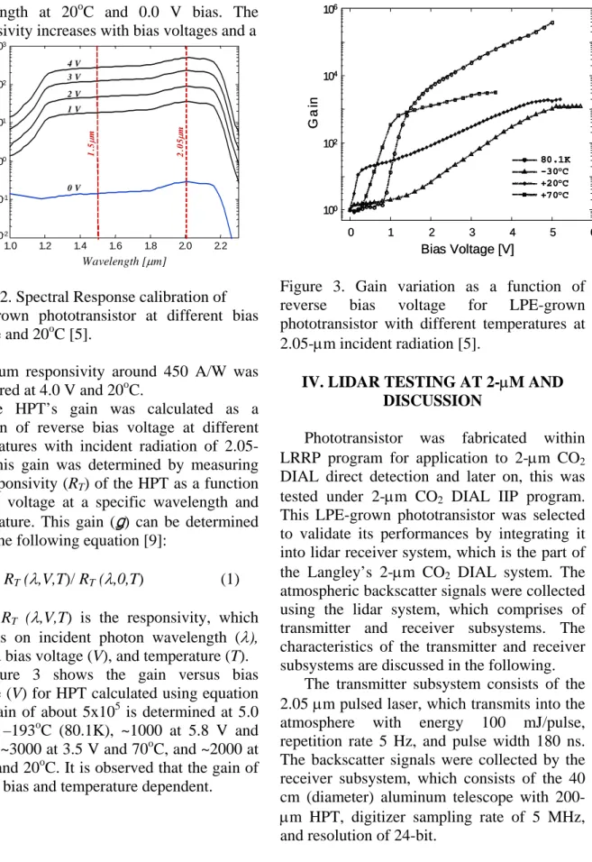
NASA LaRC detector group carried out comprehensive device characterization, including responsivity, dark current, and noise measurements and determined quantum efficiency and NEP. The HPT was integrated into an ILX Lightwave chamber with cooling system. Figure 2 shows the responsivity variation with wavelength in the 1.0- to 2.3-µm range of 200-µm diameter phototransistor [5]. The result shows cutoff wavelength at
2.2-µm with operating temperature at 20oC and different bias voltages. The peak responsivity around 0.25 A/W was detected at 2.0-µm
wavelength at 20oC and 0.0 V bias. The responsivity increases with bias voltages and a
1.0 1.2 1.4 1.6 1.8 2.0 2.2 10-2 10-1 100 101 102 103 Wavelength [µm] R e sp o n si v it y [A /W ] 0 V 1 V 2 V 3 V 4 V 2. 0 5 µ m 1. 5 µ m
Figure 2. Spectral Response calibration of LPE-grown phototransistor at different bias voltage and 20oC [5].
maximum responsivity around 450 A/W was monitored at 4.0 V and 20oC.
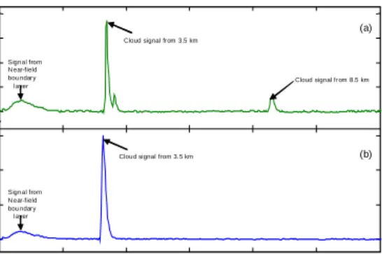
The HPT’s gain was calculated as a function of reverse bias voltage at different temperatures with incident radiation of 2.05-µm. This gain was determined by measuring the responsivity (RT) of the HPT as a function
of bias voltage at a specific wavelength and temperature. This gain (
ǥ
) can be determined using the following equation [9]:ǥ
= RT (λ
,V,T)/ RT (λ
,0,T) (1)where RT (
λ
,V,T) is the responsivity, whichdepends on incident photon wavelength (
λ
), applied bias voltage (V), and temperature (T).Figure 3 shows the gain versus bias voltage (V) for HPT calculated using equation 1. A gain of about 5x10⁵ is determined at 5.0 V and –193oC (80.1K), ~1000 at 5.8 V and
−30oC, ~3000 at 3.5 V and 70oC, and ~2000 at 5.2 V and 20oC. It is observed that the gain of HPT is bias and temperature dependent.
0 1 2 3 4 5 6 100 102 104 106 Bias Voltage [V] Ga in 80.1K -30oC +20oC +70oC 0 1 2 3 4 5 6 100 102 104 106 Bias Voltage [V] Ga in 80.1K -30oC +20oC +70oC 80.1K -30oC +20oC +70oC
Figure 3. Gain variation as a function of reverse bias voltage for LPE-grown phototransistor with different temperatures at 2.05-µm incident radiation [5].
IV. LIDAR TESTING AT 2-µM AND
DISCUSSION
Phototransistor was fabricated within LRRP program for application to 2-µm CO2
DIAL direct detection and later on, this was tested under 2-µm CO2 DIAL IIP program.
This LPE-grown phototransistor was selected to validate its performances by integrating it into lidar receiver system, which is the part of the Langley’s 2-µm CO2 DIAL system. The
atmospheric backscatter signals were collected using the lidar system, which comprises of transmitter and receiver subsystems. The characteristics of the transmitter and receiver subsystems are discussed in the following.
The transmitter subsystem consists of the 2.05 µm pulsed laser, which transmits into the atmosphere with energy 100 mJ/pulse, repetition rate 5 Hz, and pulse width 180 ns. The backscatter signals were collected by the receiver subsystem, which consists of the 40 cm (diameter) aluminum telescope with
200-µm HPT, digitizer sampling rate of 5 MHz, and resolution of 24-bit.
This HPT was utilized to record the atmospheric returns and analyzed their features. The HPT attached with thermo-electric cooler (TEC) and trans-impedance amplifier was integrated into 2-µm CO2 DIAL
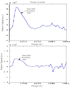
system. TEC was used to operate the HPT at fixed temperature (20oC). Lidar system was aligned using a 3.5 km thin cloud as target, as specified in signal profiles for both return signals in Figures 4a and 4b. The atmospheric returns in Figure 4 are represented by the digitizer output in volt converted into counts (e-/µsec) in the vertical axis and the digitizer samples converted into range (km) in the horizontal axis.
Lidar system was pointed vertically to collect atmospheric returns through HPT. The return signals from thin clouds were detected at two different times by the HPT and Figure 5a (Top trace) showed two-layer thin cloud signals at 3.5 km and 8.5 km distances through HPT and near-field boundary layer signals were also obtained. Figure 5b (Bottom trace) showed signals from one-layer thin cloud at 3.5 km and near field boundary layer ~0.2 - 1.3 km distances. It was observed that small amplitude signal from top cloud layer was detected by the phototransistor, but relatively large signal from the bottom layer cloud target was monitored by the same HPT.
Range [km] 0 1 2 3 4 0 2 4 6 8 10 12 0 2 4 6˜ R e tu rn S ign al [ ×1 0 5e -/µ s ] Sign al from N ear-field bou ndary l ayer
Cloud signal from 3.5 km
Cloud signal from 8.5 km
(a)
(b)
Clou d signal from 3.5 km Sign al from N ear-field bou ndary l ayer Range [km] 0 1 2 3 4 0 2 4 6 8 10 12 0 2 4 6˜ R e tu rn S ign al [ ×1 0 5e -/µ s ] Range [km] 0 1 2 3 4 0 2 4 6 8 10 12 0 2 4 6˜ R e tu rn S ign al [ ×1 0 5e -/µ s ] Sign al from N ear-field bou ndary l ayer
Cloud signal from 3.5 km
Cloud signal from 8.5 km
(a)
(b)
Clou d signal from 3.5 km Sign al from
N ear-field bou ndary l ayer
Figure 4. Atmospheric return signals using HPT.
Figure 5 shows atmospheric features of the return signals for the HPT. The system was
pointed at thin discrete clouds at about 3.5 - 9.0 km altitudes. The color image represents the backscattered range corrected signal. The time scale represents the time span between 0.0 to 550 sec, which corresponds to the phototransistor operating time at a temperature of 20oC. Near-field boundary layer was observed between the 0.2 km and 1.3 km and this shows potential application of the phototransistor for lidar remote sensing.
Time (s) Al ti tu d e ( m ) 1 0 0 2 0 0 3 0 0 4 0 0 5 0 0 3.5 km cloud layer Near-field boundary-layer 8.5 km cloud layer 1 0 0 2 0 0 3 0 0 4 0 0 5 0 0 1 0 0 2 0 0 3 0 0 4 0 0 5 0 0 3.5 km cloud layer Near-field boundary-layer 8.5 km cloud layer
Figure 5. Atmospheric images using HPT. The APD with cryogenic dewar and trans-impedance amplifier was integrated into the
2-µm lidar system. Dewar was used to operate the APD at cryogenic temperature (78K). Figure 6 shows atmospheric return signals through the APD and HPT. The signals presented in this figure were analyzed with range correction ((S-B)*R2, where S is the signal, B is the background, and R is the range). The range spans between 0.0 to 4.0 km altitudes in the horizontal axis. Results show near-field boundary layer from 100 to 1400 m, but some noise observed in the range of 2000 to 4000 m as indicated in Figure 6, which might be due to the transimpedance amplifier problem of the APD’s associated electronics including noise of MBE-grown APD and also HPT.
Finally, the HPT and APD were developed for 2-µm wavelength operation and utilized for evaluation of their performances. Preliminary results show that LPE-grown phototransistor has a compatible performance in the boundary
layer region (100 to 1400 m) with respect to HgCdTe APD at 2.0-µm wavelength.
Figure 6. Atmospheric return signals using 2-µm HPT (Top trace) and HgCdTe APD (Bottom trace).
V. SUMMARY
AlGaAsSb/InGaAsSb HPTs were developed at Astropower, Inc. and were characterized at NASA Langley Research Center. Results obtained including high responsivity, high gain, and relatively low NEP were reported in the following references [2,4,6-7].
The phototransistor, which was integrated into the lidar system, was developed and optimized for 2-µm wavelength operation. Lidar measurements included detecting atmospheric structures consisting of thin clouds in the mid-altitude and near-field boundary layer. These test results are very promising for the application of phototransistors to the two-micron lidar remote sensing. This phototransistor also showed compatible performance with respect to HgCdTe APD operating at 2.0-µm.
ACKNOWLEDGEMENT
This work is supported by Laser Risk Reduction Program and 2-µm CO2 DIAL IIP
Project under NASA’s Earth Science Technology Office and NASA’s Enabling Concepts & Technologies Program. The authors would like to thanks Oleg Sulima from University of Delaware for fabricating the phototransistors. The authors also acknowledge George Komar, William Stabnow, and Michael Kavaya for their constant support.
REFERENCES
[1] S. Ismail, G. J. Koch, B. W. Barnes, N. Abedin, T. F. Refaat, J. Yu, S. A. Vay, S. Kooi, E.V. Browell, U. N. Singh,
Technology Developments for Tropospheric Profiling of CO2 and
Ground-based Measurements, Proceedings of the 22nd International Laser Radar Conference, 65-68 (2004).
[2] T.F. Refaat, M.N. Abedin, O.V. Sulima, S. Ismail, and U.N. Singh,
“AlGaAsSb/InGaAsSb phototransistors for 2-µm remote sensing applications”,
Optical Engineering 43(7), 1647-1650 (2004).
[3] T.F. Refaat, M.N. Abedin, O.V. Sulima, U.N. Singh, and S. Ismail, Novel infrared phototransistors for atmospheric CO2
profiling at 2 µm wavelength, IEDM Tech. Dig., 355-358 (2004).
[4] O.V. Sulima, T.F. Refaat, M.G. Mauk, J.A. Cox, J. Li, S.K. Lohokare, M.N. Abedin, U.N. Singh, and J.A. Rand, AlGaAsSb/InGaAsSb phototransistors for spectral range around 2-µm, Electronics Letters 40, 766-767, (2004).
[5] T.F. Refaat, M.N. Abedin, O.V. Sulima, S. Ismail, and U.N. Singh, “III-V compound detectors for CO2 DIAL measurements”, Proc. of SPIE Vol. 5887, p. 588706-1,
2007.
[6] M.N. Abedin, T.F. Refaat, O.V. Sulima, and U.N. Singh, “AlGaAsSb/InGaAsSb heterojunction phototransistors with high optical gain and wide dynamic range”, IEEE Trans. Electron Devices 51(12), 2013-2018 (2004).
[7] M.N. Abedin, T.F. Refaat, O.V. Sulima, and U.N. Singh “Recent development of Sb-based phototransistors in the 0.9- to 2.2-µm wavelength range for applications to laser remote sensing”, Int. J. High Speed Electronics and Systems, Vol. 16 (2), pp. 567-582 (2006).
[8] T.F. Refaat, S. Ismail, T. Mack, M.N. Abedin, S. Mayor, S. Spuler, and U.N. Singh, “Infrared phototransistor validation for atmospheric remote sensing application using the Raman-shifted eye-safe aerol
lidar”, Optical Engineering, 46(8), p. 086001, (2007).
[9] M.N. Abedin, T.F. Refaat, S. Ismail, and U.N. Singh, “Phototransistors development and their applications to Lidar”, presented at the NASA Science Technology
Conference, 2007.
[10] S. Ismail, G. J. Koch, M.N. Abedin, T. F. Refaat, M. Rubio, and U.N. Singh,
“Development of Laser, Detector, and Receiver Systems for an Atmospheric CO2
lidar profiling System”, presented at the NASA Science Technology Conference, 2007.
[11] M.N. Abedin, T.F. Refaat, O.V. Sulima, S. Ismail, and U.N. Singh, “Two-micron detector development using Sb-based material systems”, presented at the NASA Science Technology Conference, 2006.
![Figure 1. Phototransistor structure of the fabricated AlGaAsSb/InGaAsSb material system on GaSb substrate [4]](https://thumb-us.123doks.com/thumbv2/123dok_us/1762782.2750131/2.918.546.790.466.626/figure-phototransistor-structure-fabricated-algaassb-ingaassb-material-substrate.webp)