Theses & Dissertations Boston University Theses & Dissertations
2019
A multi-layer approach to designing
secure systems: from circuit to
software
https://hdl.handle.net/2144/36149
COLLEGE OF ENGINEERING
Dissertation
A MULTI-LAYER APPROACH TO DESIGNING SECURE
SYSTEMS: FROM CIRCUIT TO SOFTWARE
by
BOYOU ZHOU
B.S., Southeast University, China, 2013
M.S., Boston University, 2019
Submitted in partial fulfillment of the
requirements for the degree of
Doctor of Philosophy
2019
First Reader
Ajay J. Joshi, PhD
Associate Professor of Electrical and Computer Engineering
Second Reader
Manuel Egele, PhD
Assistant Professor of Electrical and Computer Engineering
Third Reader
M. Selim ¨Unl¨u, PhD
Professor of Electrical and Computer Engineering Professor of Materials Science and Engineering Professor of Biomedical Engineering
Fourth Reader
Gianluca Stringhini, PhD
First, I would like to express my gratitude to my advisor, Ajay Joshi. This work would not have been possible without Ajay’s guidance and help. I am also thankful to Prof. Manuel Egele, as my co-advisor, for the last three years. He advised and guided most of my works during this process. My regret throughout the entire graduate school was to get to know him sooner. I also appreciate the help from Prof. Selim Unlu, for the guidance in our photonic project. I want to thank the funding agency, NSF and DARPA, to support all my works.
It goes without saying, without support from my parents, Jianhua Zhou, and Qi Jin, this work is not possible. Also, my girlfriend, Weisi Liao, was also incredibly supportive to help me through this process.
I also want to thank my collaborators, Ronen Adato, Aydan Aksoylar, Anmol Gupta, Rasoul Jahanshahi, Negin Zaraee, and Sadulla Canakci. With their collabo-rations, I could finish the works and publish them in the past few years. I would like to thank Boston University for funding most of my works and DARPA for the Posh open source hardware project (POSH). I also appreciate my colleagues in our group: Leila, Zahra, Yenai, Furkan, Marcia, Saiful, Zafar, Mahmoud, Schuyler, and Chao. I would never forget the life with them, the life sharing all happiness. This goes to the PEAC and CAAD labs too.
SYSTEMS: FROM CIRCUIT TO SOFTWARE
BOYOU ZHOU
Boston University, College of Engineering, 2019
Major Professors: Ajay J. Joshi, PhD
Associate Professor of Electrical and Computer
Engineering
Manuel Egele, PhD
Assistant Professor of Electrical and Computer
Engineering
ABSTRACT
In the last few years, security has become one of the key challenges in computing systems. Failures in the secure operations of these systems have led to massive in-formation leaks and cyber-attacks. Case in point, the identity leaks from Equifax in 2016, Spectre and Meltdown attacks to Intel and AMD processors in 2017, Cyber-attacks on Facebook in 2018. These recent Cyber-attacks have shown that the intruders attack di↵erent layers of the systems, from low-level hardware to software as a service (SaaS). To protect the systems, the defense mechanisms should confront the attacks in the di↵erent layers of the systems. In this work, we propose four security mech-anisms for computing systems: (i) using backside imaging to detect Hardware Tro-jans (HTs) in Application Specific Integrated Circuits (ASICs) chips, (ii) developing energy-efficient reconfigurable cryptographic engines, (iii) examining the feasibility of malware detection using Hardware Performance Counters (HPC).
Most of the threat models assume that the root of trust is the hardware running vi
leak confidential information. HTs inserted during fabrication are extremely hard to detect since their overheads in performance and power are below the variations in the performance and power caused by manufacturing. In our work, we have developed an optical method that identifies modified or replaced gates in the ICs. We use the near-infrared light to image the ICs because silicon is transparent to near-near-infrared light and metal reflects infrared light. We leverage the near-infrared imaging to identify the locations of each gate, based on the signatures of metal structures reflected by the lowest metal layer. By comparing the imaged results to the pre-fabrication design, we can identify any modifications, shifts or replacements in the circuits to detect HTs.
With the trust of the silicon, the computing system must use secure communica-tion channels for its applicacommunica-tions. The low-energy cost devices, such as the Internet of Things (IoT), leverage strong cryptographic algorithms (e.g. AES, RSA, and SHA) during communications. The cryptographic operations cause the IoT devices a sig-nificant amount of power. As a result, the power budget limits their applications. To mitigate the high power consumption, modern processors embed these cryptographic operations into hardware primitives. This also improves system performance. The hardware unit embedded into the processor provides high energy-efficiency, low en-ergy cost. However, hardware implementations limit flexibility. The longevity of the IoTs can exceed the lifetime of the cryptographic algorithms. The replacement of the IoT devices is costly and sometimes prohibitive, e.g., monitors in nuclear reactors. In order to reconfigure cryptographic algorithms into hardware, we have developed a system with a reconfigurable encryption engine on the Zedboard platform. The hardware implementation of the engine ensures fast, energy-efficient cryptographic operations.
the use of the Hardware Performance Counters (HPCs) in malware detection. HPCs are hardware units that count micro-architectural events, such as cache hits/misses and floating point operations. Anti-virus software is commonly used to detect mal-ware but it also introduces performance overhead. To reduce anti-virus performance overhead, many researchers propose to use HPCs with machine learning models in malware detection. However, it is counter-intuitive that the high-level program be-haviors can manifest themselves in low-level statics. We perform experiments using 2⇠3 ⇥larger program counts than the previous works and perform a rigorous anal-ysis to determine whether HPCs can be used to detect malware. Our results show that the False Discovery Rate of malware detection can reach 20%. If we deploy this detection system on a fresh installed Windows 7 systems, among 1,323 binaries, 198 binaries would be flagged as malware.
1 Introduction 1
1.1 Background and Motivation . . . 1
1.2 Related Work . . . 5
1.2.1 HT Detection using Backside Imaging . . . 6
1.2.2 Cryptographic Engines for IoT Devices . . . 8
1.2.3 Malware Detection using Hardware Performance Counters with Machine Learning . . . 10
1.3 Completed Research . . . 14
2 Hardware Trojan Detection Using Backside Imaging 17 2.1 Introduction . . . 17
2.2 Threat Model . . . 20
2.3 Backside Imaging of IC Chips . . . 20
2.3.1 Optical Imaging Method . . . 22
2.3.2 Technology Scalability . . . 25
2.3.3 Optical Simulation Methodology . . . 26
2.4 HT Detection Process . . . 28
2.4.1 Methodology to Generate “Golden Reference” . . . 28
2.4.2 Correlation Method . . . 31
2.4.3 Results . . . 32
2.5 Noise-Based Detection Method . . . 33
2.5.1 Methodology Explanation . . . 34
2.6.1 Process Variation . . . 38
2.6.2 Resolution and Window Size . . . 39
2.6.3 Pattern Insertion . . . 40
2.6.4 Results . . . 41
2.7 Nanoantenna Implementations . . . 43
2.8 Conclusion . . . 44
3 Cryptographic Algorithms on a Programmable SoC for IoT Devices 54 3.1 Introduction . . . 54
3.2 Threat Model . . . 58
3.3 Background . . . 58
3.3.1 Cryptographic Algorithms . . . 58
3.3.2 Cryptographic Accelerators . . . 59
3.3.3 A case for FPGA based Crypto . . . 61
3.4 Experimental Setup . . . 62 3.5 Evaluation . . . 66 3.5.1 Symmetric Cryptography . . . 67 3.5.2 Asymmetric Cryptography . . . 68 3.5.3 Hash Function . . . 68 3.6 Conclusion . . . 68
4 Malware Detection using Hardware Performance Counters with Ma-chine Learning 75 4.1 Introduction . . . 75
4.2 Threat Model . . . 79
4.3 Experimental Setup . . . 79
4.3.3 Method for Running Experiments . . . 82
4.4 Machine Learning Models . . . 84
4.4.1 Reduction of Dimensions . . . 84 4.4.2 Selection of Events . . . 86 4.4.3 Classification Models . . . 91 4.5 Experimental Results . . . 94 4.5.1 Malware Detection . . . 96 4.5.2 Cross-Validation . . . 100 4.5.3 Ransomware . . . 103 4.6 Discussion . . . 104 4.7 Conclusion . . . 104
5 Conclusions and Future Work 106 5.1 Hardware Trojan Detection using near-Infrared Backside Imaging . . 106
5.2 High-Performance Low Energy Implementation of Cryptographic Al-gorithms on a Programmable SoC for IoT Devices . . . 108
5.3 Malware Detection using Hardware Performance Counters with Ma-chine Learning . . . 109
References 111
Curriculum Vitae 124
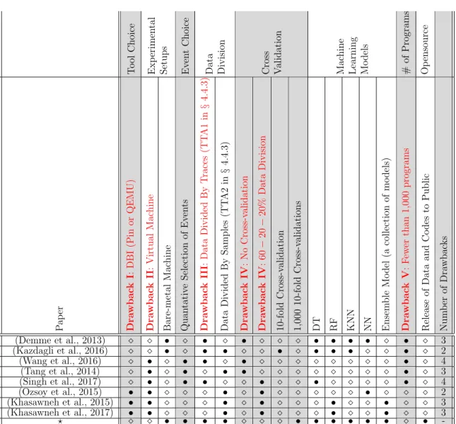
1.1 Comparison between various previous works: Rows are various works in HPC-based malware detection and columns are design choices. The alternative shaded and white background represents di↵erent categories of tool/setup/model in malware detection using HPCs. Red texts high-light drawbacks, and black texts express the suggested tool/setup/model from this work. Solid dots (•) indicate the use of that tool/setup/model (column) by the reference (row), and hollow dimonds (⇧) indicate the non-use of that tool/setup/model by the reference. Star (?) is our work. Our work avoids the drawbacks discussed in the table, and quantita-tively analyzes how these drawbacks lead to the conclusion that HPCs can reliably detect hardware. . . 12 2.1 Area (in µm2) In this table, we show power consumption of all the
testbenches that we implemented in this paper. . . 33 2.2 Area of Inserted fill cells[µm2], 0.19, 0.38, 0.57 represents the width of
each fill cell in the array in [µm], 1, 2, 3, 4 represents number of rows and columns of the array. . . 42 3.1 This table shows the LUTs utilizations in FPGA of di↵erent
crypto-engines. . . 66 4.1 Description of the Selected Events (AMD, 2015) . . . 90
2·1 Backside Imaging of IC chips . . . 21 2·2 (a) The reflectance spectrum of functional gates and fill cells designed
in 45 nm technology (computed via FDTD simulations). The response is computed for both X and Y polarizations of the illuminating field (solid and dashed lines, respectively). For X polarization, the incident electric field is polarized along the VDD and VSS rails. For Y polariza-tion, the polarization is perpendicular. (b) The reflectance spectrum of functional gates and fill cells designed using 15nm technology. Fill cells still show much higher reflectance compared to functional cells. 24 2·3 (a) Physical layout of a 10µm⇥10µmregion of the AEST100 hardware
block. (b) Backside image (reflectance value) of the 10µm⇥ 10µm
region. The fill cells have the highest reflectance. . . 29 2·4 (a) Backside image (reflectance value) of the 10µm ⇥ 10µm region
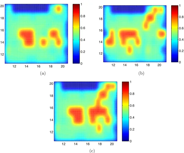
where the fill cells are replaced with functional gates that constitute the HTs. (b) Backside image (reflectance value) of the 10µm⇥10µm
region where the bottom 3 rows are shifted by 5µm to the left to make room for cells that constitute the HT. (c) Backside image (reflectance value) of the 10µm⇥10µmregion when the functional cells are replaced by a di↵erent set of cells that constitute the HT. . . 30
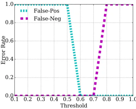
rates versus threshold. The optimized detection threshold should be 0.65 for a fixed SNR of 10. . . 32 2·6 (a) shows false negative error rates versus SNR of c1908 and c499
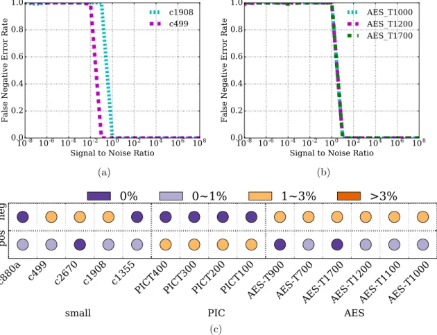
test-benches from (Wei et al., 2012a) using correlation comparison method. (b) shows AES-T1000, AES-T1200, and AES-T1700 testbenches from (Tru, 2014) using correlation comparison method. (c) is a summary of vari-ous testbenches from both (Wei et al., 2012a) and (Tru, 2014). We use colors in the legend to denote the error rates at SNR from 10 8 to 0.1 belonging to the corresponding range. . . 46 2·7 (a) shows part of reflectance layout in testbench c1355. We use single
gate FDTD results of the optical responses to represent every pixels in the gate location. (b) shows the cubic interpolated results from (a) as the reference of non-tampered circuit, which we denote it MY. (c) is AWGN with a variant 0.01 of the same area. (d) is one tampered circuit example, in which we replace one NAND gate with an AND gate. We use the measure response, MY, subtracted by the ”golden reference”, MX, to get the image in (d). . . 47 2·8 (a) shows false negative error rates versus SNR of two testbenches
from (Wei et al., 2012a) using noise detection method. (b) shows three testbenches from (Tru, 2014) using noise detection method. (c) is a summary of various testbenches from both (Wei et al., 2012a) and (Tru, 2014). We use colors in the legend to denote the error rates at SNR from 10 8 to 0.1 belonging to the corresponding range. . . . 48
laser reflectance is on the left and Y polarization laser reflectance is on the right.The thick red line represents the process variation free reflectance of XOR2 X1 cell. The other lines are the reflectance with process variation. . . 49 2·10 (a) Process variation free XOR2 X1 gate. (b) XOR2 X1 with 10%
process variation in the X dimension. Here, all the metal structures inside of the gate have been compressed by 10% on the X dimension to model process variations. . . 50 2·11 Fill cell pattern that we inserted before place&route of the design.
We put this array of fill cells to secure these regions from shifts or replacements of fill cells and replacement of functional cells with other set of functional cells. . . 51 2·12 (a) shows false negative error rates versus SNR of three testbenches
from (Tru, 2014) with an imaging resolution of 0.1µm. (b) shows three of testbenches from (Tru, 2014) using noise detection method with an imaging resolution of 0.2µm. (c) is a summary of various testbenches from both (Wei et al., 2012a). We use colors in the legend to denote the error rates at SNR from 10 8 to 0.1 belonging to the corresponding range. Here, 10, 20, and 30 refer to detection window sizes 10µm, 20µm, 30µm, On the X axis, 0.1, 0.2, and 0.4 refer to resolutions of the image as 0.1µm, 0.2µm, and 0.4µm, respectively. . . 52
of fill cell arrays. On the y axis, the number represents number of rows and columns that we used in fill cell array. On the x axis, the number represents the size of fill cells in the array. . . 53 2·14 (a) shows the metal 1 layer of the AND and NAND gate pair. (b)
shows the metal 1 layer of the AND and NAND with 322 nm distances between metal structures and 200 nm nano-antenna between the two gates . . . 53 3·1 System Architecture for AES Encryption Engine . . . 62 3·2 Figures show the comparisons between C implementation (software),
and FPGA implementation (hardware) of DES in encryption (ENC) and decryption (DEC). We encrypt and decrypt ranging from 16 blocks to 166 blocks. (a) and (b) show time comparisons. Encryption shows 1.9⇥ faster and decryption is 1.6⇥ faster. (c) and (d) show power consumption and energy comparisons. Encryption has 3.9⇥ energy reduction and decryption has 1.9⇥energy reduction. (e) and (f) show EDP comparisons. Encryption has 7.6⇥ savings and decryption has 3.0⇥savings. We can see performance boost, energy savings and EDP reductions of hardware implementation in DES. . . 70
tion (ENC) and decryption (DEC). We encrypt and decrypt ranging from 1 block to 107 blocks. (a) and (b) show time comparisons. En-cryption is 18.8⇥ faster and decryption is 116.6⇥ faster. (c) and (d) show power consumption and energy comparisons. Encryption has 13.9⇥ energy reduction and decryption has 6.0⇥ energy reduction. (e) and (f) show EDP comparisons. Encryption has 261.9⇥ savings and decryption has 704.6⇥ savings. We can see orders of magnitude performance boost, energy savings and EDP reductions of hardware implementation in AES ECB mode. . . 71 3·4 Figures show the comparisons between C implementation (software),
and FPGA implementation (hardware) of AES block cipher modes, for both CBC and GCM. In all the hardware implementations, AES core engine operations use FPGA, while block cipher modes use c imple-mentation. Thus, we still can see significant performance boost and energy savings in CBC modes, while much less benefits in GCM modes. In CBC mode, we encrypt and decrypt data ranging from 1 block to 107 blocks. In GCM mode, we encrypt data ranging from 4 to 40 blocks. (a), (b) and (g) show time comparisons. CBC encryption is 6.3⇥ faster, CBC decryption is 38.6⇥ and GCM is 1.1⇥ faster. (c), (d) and (h) show power consumption and energy comparisons. CBC encryption has 33.2⇥ energy reduction, CBC decryption has 154.8⇥ energy reduction and GCM has 1.2⇥ energy reduction. (e), (f) and (i) show EDP comparisons. CBC encryption has 82.4⇥ savings, CBC decryption has 233.4⇥ savings, and GCM has 1.3⇥ savings. . . 72
and decryption (DEC). We encrypt and decrypt ranging from 1 block to 105 blocks. (a) and (b) show time comparisons. Encryption is 71.2⇥faster and decryption is 2983.1⇥ faster. (c) and (d) show power consumption and energy comparisons. Encryption has 6.5⇥ energy reduction and decryption has 4033.0⇥ energy reduction. (e) and (f) show EDP comparisons. Encryption has 462.7⇥ savings and decryp-tion has 12,000,000 +⇥ savings. We can great performance boost, energy savings and EDP reductions of hardware implementation in RSA decryption, since RSA private key length is much longer than public key length. . . 73 3·6 Figures show the comparisons between C implementation (software),
and FPGA implementation (hardware) of SHA. We do hash ranging from 16 blocks to 166 blocks. (a) show time comparisons. (b) show power consumption and energy comparisons. (c) show EDP compar-isons. We can see performance boost, energy savings and EDP reduc-tions of hardware implementation in SHA. It shows 6.6⇥faster in time, 4.6⇥ reduction in energy, and 30.3⇥ savings in EDP. . . 74
worker node spawns aSavitor process, and thenSavitor runs the target process (benignware/malware). The dotted arrow (99K) means that the action does not always happen. If the application has a window for interaction, we attach a monkey tester to the window. The solid arrow (!) shows that actions always happen. We reset the environment after each experiment. the worker node kills any other processes spawned by the target process after each benignware experiment. At the end of each malware experiment, we reboot the machine into the Debian partition to reload a clean Windows image. . . 82
benignware. The dashed line is the mean of each distribution. The boxes represent 25% ⇠ 75% of the distributions. The whiskers (the short, horizontal lines outside the boxes) represent the confidence inter-val equiinter-valent toµ±3 of Gaussian Distribution (0.3% ⇠99.7%). We measure The number of Load operations dispatched to the Load-Store unit event 5 times in one benignware (creative2 from Futuremark) and one malware. The distributions of the two subplots represent 5 exam-ples in the experiments. (a) Distributions of sampled values before the reduction of dimensions: We cannot distinguish between the 5 malware examples and the 5 benignware examples. (b) Distributions of sampled values after the reduction of dimensions: We apply the reduction of di-mensions to examples in (a) to get examples in (b). We can separate all the examples in (b) due to the gaps between values of malware and benignware in both features. . . 85 4·3 Error Bound vs the Number of Eigenvetors Plot: when choosing
dif-ferent number of eigenvectors for reduction in dimensions, the error bound ↵ changes according tom eigenvectors. . . 89 4·4 Receiver Operating Characteristic (ROC) curve of 5 models. (a) The
AUC of DT, NN, AdaBoost, RF, and KNN using (TTA1) is 89.65%, 84.41%, 80.57%, 91.84%, and 89.26%, respectively. (b) The AUC of DT, NN, AdaBoost, RF, and KNN using (TTA2) is 87.36%, 66.43%, 77.96%, 89.94%, and 86.98%, respectively. . . 95
corresponds to cross-validation experiment results that lie between 25 and 75 percentiles. The whiskers (the short, horizontal lines outside the blue box) represent confidence interval equivalent to µ±3 of a Gaussian Distribution. The blue dots are outliers that are outside the
µ±3 regime. On the X-axis, Prec is precision, Rec is recall, and F1 is F1 score. AUC is area under curve in ROC. These 10-fold cross-validation experiments show that we cannot achieve 100% malware detection accuracy. . . 99
AEAD . . . Authenticated Encryption with Associated Data AES . . . Advanced Encryption Standard
ASLR . . . Address-Space-Layout-Randomization AUC . . . Area Under Curve
AXI . . . Advanced eXtensible Interface CDF . . . Cumulative Distribution Function CFG . . . Control Flow Graph
CFI . . . Control Flow Integrity
DBI . . . Dynamic Binary Instrumentation DEP . . . Data Execution Prevention DES . . . Data Encryption Standard DPA . . . Di↵erential Power Analysis DT . . . Decision Tree
ECB . . . Electronic Code Book mode ECs . . . Equivalence Classes
GPP . . . General Purpose Processor GRUB . . . GNU GRand Unified Bootloader HPC . . . Hardware Performance Counter HPCs . . . Hardware Performance Counters HTs . . . Hardware Trojans
IoTs . . . Internet of things
IR . . . Intermediate Representations
ITLB . . . Instruction Translation Lookaside Bu↵er JIT . . . Just-In-Time
KNN . . . K Nearest Neighbors MLP . . . Multilayer Perceptron NN . . . Neural Net
NSA . . . National Security Agency NX . . . Non-Executable memory PCA . . . Principal Component Analysis PDF . . . probability density function
POSH . . . Posh open source hardware project POSIX . . . Portable Operating System Interface RE . . . Reverse Engineer
RF . . . Random Forest xxiii
SHA . . . Secure Hash Algorithm SNR . . . Signal to Noise Ratio SoC . . . System on Chip SSH . . . Secure SHell
TSVs . . . Through Silicon Vias
TTA . . . Training-and-Testing Approach VLIW . . . Very Long Instruction Word
Chapter 1
Introduction
1.1
Background and Motivation
In the last few years, the security of the computing systems has become one of the main concerns in our lives. In 2016, identity theft from Equifax leaked the social security numbers of 300 million people (Equ, 2019); Spectre and Meltdown in 2017 a↵ected all Intel and AMD processors to show the vulnerabilities in the architectural level (Mel, 2019); The leak of information from Facebook in 2018 directly a↵ected millions of user profiles (Fac, 2019). Every year, there were a series of events in the security area involving millions or even billions of people. The previous incidents have shown that the security attacks have reached regimes which cannot be tackled by the existing defense system. Spectre and Meltdown exposed security flaws in computer architecture. The leaks of Facebook user profiles illustrated that the attacks on web applications can have social and political e↵ects. In order to mitigate these failures in the existing systems, there is a pressing need to build secure systems on every layer of the computing systems, from circuits to web applications.
The root of the trust in the defense systems is the silicon running beneath all the software stacks. In general, the fabless design companies, such as Qualcomm, ARM and Broadcom trust the manufacturers of the ICs. The hardware companies fabricate their IC chips overseas, given that overseas IC manufacturers can support a range of technology nodes at much lower cost (AsC, 2019). However, this trust has been broken since the separation of design and manufacturing creates opportunities for hardware
attacks like Hardware Trojan (HT) insertion, IC overbuild, reverse engineering, side-channel analysis, and IC counterfeiting (Tehranipoor and Koushanfar, 2010). Among these attacks, HTs can cause significant economic and social damages. HTs are hardware blocks that are designed to perform malicious operations, e.g. leak secret keys, sabotage the functionality of the chip or launch privilege escalation attacks on the system. The HTs inserted during manufacturing have negligible overheads in performance and power consumption of the overall ICs (Nowroz et al., 2014; Yang et al., 2016). Besides, the attackers design HTs to evade being triggered during functional testing (Wei et al., 2012a). IC design companies need to either monitor the entire manufacturing process or apply costly reverse engineering techniques, including delayering the chip, imaging with Scanning Electron Microscope (SEM) etc. to detect HTs (Tehranipoor and Koushanfar, 2010; Karri et al., 2010). Both delayering and SEM are time-consuming and costly. Hence, there is a pressing need for a detection method, which can detect and locate HTs inserted during fabrication stage in a fast, accurate, and robust manner (Tsoutsos and Maniatakos, 2014).
At the architectural level, the security functionalities, e.g. cryptographic opera-tions, ensure the confidentiality and integrity of the communications. The architec-tural solutions are deployed using dedicated Application Specific Integrated Circuit (ASIC) units embedded within the processor. For example ARM, Intel, and AVR, all provide hardware accelerated Advanced Encryption Standard (AES), crypto-engines in their ARMv8 (ARM, 2016), x86 (Int, 2016a), and Atmel (AVR, 2016) platforms respectively. These processors can leverage hardware primitives to perform cryp-tographic operations, such as Advanced Encryption Standard (AES), RivestShami-rAdleman (RSA), and Secure Hash Algorithm (SHA). These operations are crucial to the Internet of things (IoT), which handle command and control signals at home and on the factory floors. IoTs are also low-power devices, which cannot easily be
replaced or modified, and are deployed for years at a time. Moreover, the longevity of these IoT devices often surpass the usage of cryptographic algorithm. Besides some IoT devices are deployed at dangerous places where they are dangerous and hard for humans to replace them. In order to achieve flexibility, high performance, and low power cryptographies, we need an energy-efficient configurable cryptography engine for IoT devices.
At the application level, the defense system must detect the malicious processes for protection. Researchers have utilized various analytical methodologies, such as signature analysis and dynamic analysis, for malware detection. All the previous methods have a substantial performance overhead. In order to reduce the overhead, the previous works propose the use of Hardware Performance Counters (HPCs) with machine learning models (Demme et al., 2013; Kazdagli et al., 2016; Wang et al., 2016; Ozsoy et al., 2015; Tang et al., 2014; Khasawneh et al., 2015; Khasawneh et al., 2017; Singh et al., 2017). HPCs are hardware blocks that count micro-architectural events. However, it is counter-intuitive that the high-level program behaviors can manifest themselves in low-level statics. In order to show the feasibility of HPC malware detection, the researchers must evaluate HPC malware detection rigorously before the real-life deployments.
In this work, we construct the solutions towards the threat models on each comput-ing layer, hardware, architectural and software layer. We present the thesis statement as following:
Constructing a defense mechanism on the same computing layer as a security threat can protect the computing system e↵ectively and effi -ciently.
Therefore, we propose a multi-level approach to securing computing systems. Our approaches include the following solutions for securing computing systems:
• HT Detection using backside imaging: We propose a novel optical method, where we image the integrated circuit chip from the backside without powering it up or delayering it (Chapter 2). Using our method, any replacements, modi-fications or re-arrangements of gates to add HTs can be easily detected through comparisons between the simulated optical response and backside imaged mea-surements. We introduce the idea of a noise-based detection method as our testing method to have higher HT detection rates in di↵erent testbenches. To further improve the robustness of our method, we strategically place high re-flectance fill cells in the designs. Our imaging method provides high-resolution, non-destructive and rapid means to detect HTs inserted during fabrication. We evaluate our approach using various hardware blocks where the HTs can occupy less than 0.1% of the total area or consist of fewer than 3 gates. In addition, we analyze our method with di↵erent magnitudes of noise, process variations, detection window sizes, and resolutions. To increase the di↵erence in the re-flection among various gates, we also engineer nano-antenna structures into the gate pairs. These nano-antennas are unique to illumination polarizations, fre-quencies and angles. By implementing the nano-antennas, we can improve the reflectance signature by 300%.
• Flexible Hardware Implementations of Cryptographies: We propose to use FPGA as the reconfigurable substrate for cryptographic operations in IoT devices (Chapter 3). We demonstrate our proposed approach on the Zedboard platform, which has two ARM cores and a Zynq FPGA. The implemented cryptographic algorithms include symmetric cryptography, asymmetric cryp-tography, and secure hash functions. We also integrate our cryptographic en-gines in the SSL library to inherit the software support for block cipher modes implemented by OpenSSL. Our approach shows that the FPGA-based
recon-figurable cryptographic components consume 1.8⇥ ⇠ 4033⇥ less energy and run 1.6⇥ ⇠2983⇥ faster than software implementation. At the same time, the FPGA implementation of cryptographic operations are more flexible compared to custom hardware implementations of cryptographic components.
• Malware Detection using Hardware Performance Counters with ma-chine learning: We identify the prevalent unrealistic assumptions and the insufficient analysis used in prior works that leverage HPCs for malware detec-tion (Chapter 4). We perform thorough experiments with a program count that exceeds prior works (Demme et al., 2013; Kazdagli et al., 2016; Wang et al., 2016; Tang et al., 2014; Singh et al., 2017) by a factor of 2⇥ ⇠ 3⇥, and the number of experiments in cross-validations that are 3 orders of magnitude more than previous works. We divide the train-and-test dataset similar to what prior works have done, as well as, in a realistic setting where testing programs are not in the training programs. We compare the e↵ects of this choice on the quality of the machine learning models. Finally, to facilitate reproducibility, and enable future researchers to easily compare their experiments with ours, we make all code, data, and results of our project publicly available under an open-source license: https://github.com/bu-icsg/Hardware_Performance_ Counters_Can_Detect_Malware_Myth_or_Fact
1.2
Related Work
In this work, we present the works related to HT detection, cryptographic engines, malware detection using HPCs with machine learning and CFI hardware enforcement.
1.2.1 HT Detection using Backside Imaging
Three di↵erent HT detection approaches have been proposed for preventing HT in-sertion and detecting any inserted HT: protective designs before fabrication, HT detection after fabrication, and side channel detection method. A number of pre-fabrication protection designs have been proposed on both circuits and architecture levels. At the circuit level, the separation of fabrication, gate level obfuscations, and limitations of gate usage have been proposed to protection designs. Separation of fabrication (Vaidyanathan et al., 2014a; Vaidyanathan et al., 2014b; Valamehr et al., 2013) proposes that the device layer of IC is fabricated by one trusted vendor, while other layers are fabricated by untrusted vendors at a lower cost. The trusted vendor use high cost Through Silicon Vias (TSVs) to connect di↵erent layers of logic. HAR-POON (Chakraborty and Bhunia, 2009) provides netlist-level obfuscation, which can be integrated into the synthesis of Soc designs. Other techniques, (Roy et al., 2008; Baumgarten et al., 2010) and (Xiao et al., 2014; Xiao et al., 2015) also provide protective designs by replacing the filler cells with functional cells. That way there are no empty spaces for inserting HTs. Bao et al. proposed to both prevent and detect HTs in (Bao et al., 2015), by limiting the useable gate types in the standard library. All these proposed techniques either use a high-cost method or sacrifice area in order to protect designs from HTs. On the architecture level, logic state scram-bling, power signatures in potential tampered logics, and circuitry encoding are the main techniques in protecting designs from HTs. ODETTE (Banga and Hsiao, 2011) protects the circuits from HTs by increasing the number and variations of the design. VITAMIN (Banga and Hsiao, 2009b) utilizes an inverted voltage scheme that aims to activate some targeted Trojans with a higher triggering rate. The power consump-tion of HTs will become prominent in the power analysis. Linear Complement Dual Codes (Ngo et al., 2015) is designed to encode the instructions inside the circuitry
and to be resistant to error injection and side channel analysis. These methods po-tentially increase the complexity of logic designs, and they also increase the power consumptions of the overall system.
Post-fabrication detection includes reverse engineer (RE), timing and power anal-ysis, and data monitoring during runtime. The generic detection method after fab-rications is to reverse engineering the fabricated ICs. Scanning Electron Microscope (SEM) and FIB (Focused Ion Beam) (Tehranipoor and Koushanfar, 2010) have been proposed for HT Detection. However, the approaches are high in cost and low in speed. The process of RE the fabricated chip is only a↵ordable to large semiconductor companies (Tehranipoor and Koushanfar, 2010; Karri et al., 2010). FANCI (Waksman et al., 2013) and FIGHT (Sullivan et al., 2014), flag possible HT wires, which reduces the complexity in reverse engineering. To detect HTs without reverse engineering the IC chips timing analyses and power analyses methods have been proposed. Timing-based analysis (Li and Lach, 2008; Jin and Makris, 2008; Exurville et al., 2015) de-tects the delay changes in the circuitry for HT Detection. Dynamic power detection, such as the sustained vector technique, measures the dynamic power consumption di↵erence in the circuitry and identifies the gates that may contain Trojans (Banga and Hsiao, 2009a; Salmani et al., 2012; Wilcox et al., 2015). Such time and power based analysis (Potkonjak et al., 2009a; Wei et al., 2010; Wei and Potkonjak, 2012; Wei et al., 2012b; Rad et al., 2008; Alkabani and Koushanfar, 2009; Potkonjak et al., 2009b; Wei and Potkonjak, 2012) are not suitable at newer technology nodes, because the impact of process variations is larger than the impact by the HTs on power and delays. This introduces overhead in the performance in order to detect HTs.
Compared to electrical methods, side channel detection utilizes physical proper-ties of ICs instead of electrical properproper-ties, which can help detect HTs that can hide from electrical tests. Emission measurements (Song et al., 2011; Stellari et al., 2014)
and thermal analysis (Nowroz et al., 2014; Forte et al., 2013) are good examples of side channel analysis. Emission measurements utilize the long wavelength imaging techniques resulting the low-resolution imaging. Thermal analysis requires the pow-ering on the logic, which introduces the enginepow-ering of testing infrastructures. All these techniques are either not as fast, easy or high in resolution as our technique.
1.2.2 Cryptographic Engines for IoT Devices
Many previous works have implemented various algorithms on the FPGA to show the performance improvements, energy savings in these FPGA implementations. The FPGA implementation of AES was first shown to have benefits on both performance improvements and energy savings in 2004 (Rouvroy et al., 2004). The performance reached a speed of 204Mbps stream in AES encryption. Since then, FPGAs were explored as a potential solution to cryptographic applications for low power devices. Good et al. proposed a design of AES, which use only on 8-bit data-path in all the operations in AES (Good and Benaissa, 2006). This design made the entire AES fit on small programmable areas. Hamalainen et al. presented an upgraded version with the cost of using 3.1k gates (Hamalainen et al., 2006). With the increasing area of FPGA, more and more resources could be used for cryptographic designs. One 128-bit AES block operation consists of key expansions and SubBytes operations. Key expansions increase the key length for further data processing in SubBytes op-erations. SubBytes is a 16-by-16 matrix operated with a minimum unit of 8-bit for permutations and substitutions during AES encryption/decryption. SubBytes opera-tions consist of substituopera-tions of cells, shifts of rows, a mix of columns and exclusive or with the keys, which are operations to increase the pseudorandomness of the output text. AES encryption/decryption usually consists of 10 ⇠ 14 rounds of SubBytes operations according to the required security level. With fully integrated SubBytes operations in hardware, AES has much higher efficiency, as AES needs fewer cycles to
finish the operations. Bulens et al. first put one full round of SubBytes operations in AES on FPGA in 2008 (Bulens et al., 2008). With pipelined designs, the plain text can be continuously streamed into the cryptographic units for encryption/decryption to achieve high throughput. Repetitive use of same hardware block cannot have the same high performance as pipelined design do since inputs in each round depend on results of previous round operations. Good et al. showed the designs from the fastest to the smallest, which can provide di↵erent design points on di↵erent hardware plat-forms, in order to achieve a trade-o↵ between speed and area (Good and Benaissa, 2005). It achieved the speed of 358Mbps compared to encryption/decryption speed of 397Mbps in our implementation without streaming throughput. Today, modern FPGAs have enough programmable logic that can fit the expansion of 10 to 14 rounds of SubBytes operations. Hoang et al. showed a fast implementation of AES with a key size of 128-bit, with look-up table of SubByteses (Hoang et al., 2012). There are also partial and dynamic reconfigurable implementations for more flexible solu-tions on FPGA (Granado-Criado et al., 2010). As partial configurasolu-tions are designed for high-end FPGA applications, low-energy FPGA has not yet widely adopted the partial configurations for their applications. Side channel attacks use power, time or other physical properties to break cryptographic algorithms. Once discovered, it is possible to prevent a given side channel attack by modifying the implementation of cryptographic algorithms. Robust designs, such as (Oswald et al., 2005; Shah et al., 2010), are resistant to Di↵erential Power Analysis (DPA) leaking AES keys in their implementation. However, robustness and DPA resistant designs come at a higher cost in performance or energy consumption. Other cryptographic algorithms, such as Hummingbird (Fan et al., 2010) and Whirlpool (Pramstaller et al., 2006), have also been implemented on FPGA. Recent works have shown that FPGA can be an ideal solution for modern cryptographic computation. Saarinen et al.
im-plemented Authenticated Encryption with Associated Data (AEAD), AES-GCM on Zedboard (Saarinen, 2014). Saarinen et al. also showed one variant implementation of Whirlpool (Saarinen and Brumley, 2014). These works contain detailed explanations of implementation and performance analysis, but lack of power and energy analysis and multi-crypto-engines implementation.
1.2.3 Malware Detection using Hardware Performance Counters with Machine Learning
Malware detection is the process of detecting malicious programs. Many previous works commonly utilize sub-semantic features in malware detection (Demme et al., 2013; Kazdagli et al., 2016; Wang et al., 2016; Ozsoy et al., 2015; Tang et al., 2014; Khasawneh et al., 2015; Khasawneh et al., 2017; Singh et al., 2017). Ozsoy et al. defined the term sub-semantic features as “micro-architectural information about an executing program that does not require modeling or detecting program seman-tics” (Ozsoy et al., 2015). These sub-semantic features are often aggregated in the HPCs to record the statistics of low-level events. All these previous works have sev-eral drawbacks to various extent. We categorize the drawbacks that we observed in the following classes.
I Dynamic Binary Instrumentation (DBI)
II Virtual Machines (VMs)
III Division of Data By Traces (TTA1 in § 4.4.3) IV No Cross-Validations or Insufficient Validations
V Few Data Samples
Besides HPCs, sub-semantic features can be extracted with dynamic binary in-strumentation (DBI) tools such as Intel’s Pin (Patil et al., 2004; Luk et al., 2005), QEMU (Bellard, 2005), Valgrind (Nethercote and Seward, 2007), or DynamoRIO (Dyn, 2017). Khasawneh, Ozsoy et al. use Pin to monitor the instructions executed on
vir-tual machines in their experimental setup (Ozsoy et al., 2015; Khasawneh et al., 2015; Khasawneh et al., 2017). Though DBI can extract sub-semantic features that are not available from HPCs, DBI introduces a substantial amount of performance overhead and is thus not suited to run in an always-on, online protection setting, which is the default use-case for current anti-malware suites. We denote the drawbacks of DBI as
Drawback I in Table 1.1.
While DBI is not feasible in online detection systems, other methods in sampling HPCs can incur inaccurate measurements. A plethora of previous works that uses HPCs for malware detections run the evaluated programs on VMs (Demme et al., 2013; Ozsoy et al., 2015; Khasawneh et al., 2015; Khasawneh et al., 2017; Singh et al., 2017). While VMs provide significant benefits to analyze unknown programs (e.g., strong isolation guarantees), HPCs are limited and shared resource between the host and all VMs. Thus, virtualizing HPCs is a challenge in itself (Serebrin and Hecht, 2011). The measured HPC values obtained in VM are substantially di↵erent from HPC values obtained from the bare-metal environment that real-life users have. To make matters worse, evasive malware can detect whether it is running in a VM and ceases to exhibit malicious behavior (Kirat et al. (Kirat et al., 2014)). These observations motivate our experimental setup (§4.3) to run all experiments on bare-metal systems. We label the use of VM in the experimental setups asDrawback II
in Table 1.1.
Due to inaccurate HPC measurements (Weaver and McKee, 2008), previous works (Demme et al., 2013; Kazdagli et al., 2016; Wang et al., 2016; Tang et al., 2014) choose to maximize the measuring granularity by using HPCs without time-multiplexing. Recall that as modern CPUs only have 6 (AMD) or 4 (Intel) registers for HPCs, malware detection methods must select the events from more than 100 available micro-architectural events (130 in AMD Bulldozer and 196 in Intel Skylake). Previous
To ol C h oi ce Ex p er im en tal S et u p s Ev en t Ch oi ce Data Divis ion Cr oss Va li d at io n Mac h in e Le arning Mo d el s # of Pr og ra m s Op ensource Pa p er D ra w ba ck I : D B I (P in or Q E M U) D ra w ba ck II : Vi rt u al M ac h in e Bare-m etal Mac h in e Quan tativ e Selection of Ev en ts D ra w ba ck II I : D at a D iv id ed B y T ra ce s (T T A1 in § 4.4.3) D at a D iv id ed B y S am p le s (T T A2 in § 4.4.3) D ra w ba ck IV : No C ro ss -v al id at io n D ra w ba ck IV :6 0 20 20% Data Division 10-fold Cross-v alidation 1,000 10-fold C ross-v alidations DT RF KNN NN En se m b le M o d el (a co ll ec ti on of mo d el s) D ra w ba ck V : F ew er th an 1, 00 0 p ro gr am s Release of Data and Co des to Public Nu m b er of D ra w b ac k s (Demme et al., 2013) ⇧ ⇧ • ⇧ • ⇧ • ⇧ ⇧ ⇧ • • • • ⇧ • ⇧ 3 (Kazdagli et al., 2016) ⇧ ⇧ • ⇧ • • ⇧ ⇧ • ⇧ • • • ⇧ ⇧ • ⇧ 2 (Wang et al., 2016) ⇧ • ⇧ • • ⇧ • ⇧ ⇧ ⇧ ⇧ ⇧ ⇧ ⇧ ⇧ • ⇧ 4 (Tang et al., 2014) ⇧ • ⇧ • ⇧ • • ⇧ ⇧ ⇧ ⇧ ⇧ ⇧ ⇧ ⇧ • ⇧ 3 (Singh et al., 2017) ⇧ • ⇧ • • ⇧ ⇧ • ⇧ ⇧ • ⇧ ⇧ ⇧ ⇧ • ⇧ 4 (Ozsoy et al., 2015) • • ⇧ ⇧ ⇧ • ⇧ • ⇧ ⇧ ⇧ ⇧ ⇧ • ⇧ ⇧ ⇧ 2 (Khasawneh et al., 2015) • • ⇧ ⇧ ⇧ • ⇧ • ⇧ ⇧ ⇧ • ⇧ ⇧ • ⇧ ⇧ 3 (Khasawneh et al., 2017) • • ⇧ ⇧ ⇧ • ⇧ • ⇧ ⇧ ⇧ • ⇧ ⇧ • ⇧ ⇧ 3 ? ⇧ ⇧ • • • • ⇧ ⇧ ⇧ • • • • • • ⇧ •
-Table 1.1: Comparison between various previous works: Rows are various works in HPC-based malware detection and columns are design choices. The alternative shaded and white background represents di↵erent categories of tool/setup/model in malware detection using HPCs. Red texts highlight drawbacks, and black texts express the suggested tool/setup/model from this work. Solid dots (•) indicate the use of that tool/setup/model (column) by the reference (row), and hollow dimonds (⇧) indicate the non-use of that tool/setup/model by the reference. Star (?) is our work. Our work avoids the drawbacks discussed in the table, and quantitatively analyzes how these drawbacks lead to the conclusion that HPCs can reliably detect hardware.
works (Demme et al., 2013; Kazdagli et al., 2016; Ozsoy et al., 2015; Khasawneh et al., 2015; Khasawneh et al., 2017) have not provided a numerical analysis of how micro-architectural events are selected. After the selection of events, we need to track these events and transform the measured HPC values to examples in machine learning models, i.e. feature extraction. Dividing examples into training and testing datasets for machine learning models are training-and-testing split. Previous works (Demme et al., 2013; Kazdagli et al., 2016; Wang et al., 2016; Singh et al., 2017) have training-and-testing split based on the examples (TTA1 in § 4.4.3) that the testing dataset can have the same examples produced by programs in the training dataset. However, in real life, it is unlikely that the o✏ine training dataset can include all the malware that a user might encounter. We mark the use of data division based on examples as
Drawback III in Table 1.1.
We observe that there is no cross-validation in some of the previous works (Demme et al., 2013; Wang et al., 2016; Tang et al., 2014), while other works (Ozsoy et al., 2015; Khasawneh et al., 2015; Khasawneh et al., 2017; Singh et al., 2017) present insufficient cross-validation, i.e. not every example in the dataset is validated. None of these works report standard deviations of detection rates with cross-validations. Without a substantial amount of cross-validation, we cannot assert the reproducibility of detection rates, since a model can have its high detection rates with specific training and testing datasets. We refer to no cross-validation or insufficient validations as
Drawback IV in Table 1.1.
Previous works reported their results with double decimal precision (Demme et al., 2013). However, double decimal precision require at least 100 experiments in test-ing. With 10-fold cross-validation in the experiments, the total number of programs (benignware and malware) should be more than 1,000 programs. Thus, at least 1,000 programs are required to evaluate the machine learning models within
numer-ical rounding error of less than 1%. There are several works that use fewer than 1,000 programs leading to over-generalization (training and testing with insufficient cross-validation), or over-interpretation of the results (comparisons beyond rounding errors) (Demme et al., 2013; Kazdagli et al., 2016; Wang et al., 2016; Tang et al., 2014; Singh et al., 2017). This insufficient number of programs in the experiments is
Drawback V in Table 1.1.
In addition to the drawbacks of the previous works, we found that there is no public access to their data or codes, which makes it hard to perform a direct comparison and examinations of the methods applied in these works.
We present all the tools/setups/models in various previous works in Table 1.1. In Table 1.1, rows are various works in HPC-based malware detection and columns are design choices of the tools/setups/models. The alternative shaded and white background represents di↵erent categories of tool/setup/model in malware detec-tion using HPCs. Red texts highlight drawbacks and black texts express the sug-gested tool/setup/model from this work. Solid dots (•) indicate the use of that tool/setup/model (column) by the reference (row), and hollow diamonds (⇧) indicate the non-use of that tool/setup/model by the reference. Star (?) is our work. The last column counts the drawbacks of the corresponding work. Table 1.1 shows that there are at least 2 drawbacks in each work.
1.3
Completed Research
The following work was completed as part of my Ph.D. Program:
• Hardware Trojan Detection using Backside Optical Imaging: In this work, we proposed to use backside optical imaging for HT detection. We first engineered fill cells to have maximum reflectance compared to standard cells. These highly reflective cells formed watermark. Any shifts, modifications to
these cells could be detected using backside imaging. By mapping the gate response to the locations and orientations of all the gates in the layout, we generated an optical response of the entire chip as the “golden response”. We applied correlation between imaged results and generated “golden reference” to determine whether the chip has HTs (Chapter 2).
We then extended our work to create a library of responses of all the cells in the standard cell library. We illuminated multiple locations on each gate according to the size of the gates to have a unique response for each gate. We improved the accuracy and robustness of our method by using noise-based detection method in the comparisons between “golden reference” and imaged results. We also did process variation analysis and optimized the detection method.
Our approach does not require costly devices as low throughput techniques, such as delayering the metal layers and SEM. Compared to the traditional electrical detection method, our method images the layouts of ICs, which does not depend on the tests that are able to trigger the HTs. The ICs under test do not need to be powered up or calibrate for testing environments, such as thermal detection method. At the same time, backside imaging presents high-resistance against process variations during manufacturing. The infrared light imaging produces images with a resolution at the gate level. No previous imaging methods have been able to achieve.
• High-Performance Low Energy Implementation of Cryptographic Al-gorithms on a Programmable SoC for IoT Devices: In this work, we implemented various kinds of cryptographies on a programmable SoC for IoT devices. We measured the performance, power and energy consumption, and re-configurability of our implementation. We implemented the same cryptographic algorithms in software and compared performance, power and energy to evaluate
the improvements achievable through hardware implementations. Our imple-mentation showed that the Zedboard platform provided high performance, low energy consumption and reconfigurability for IoT devices (Chapter 3).
Our proposed FPGA implementation can replace the implementations in the ex-isting library (OpenSSL), which enables performance boost and energy savings in various block cipher modes.
• Malware Detection using Hardware Performance Counters with Ma-chine Learning: We identify the prevalent unrealistic assumptions and the insufficient analysis used in prior works that leverage HPCs for malware detec-tion (Chapter 4). We perform thorough experiments with a program count that exceeds prior works (Demme et al., 2013; Kazdagli et al., 2016; Wang et al., 2016; Tang et al., 2014; Singh et al., 2017) by a factor of 2⇥ ⇠ 3⇥, and the number of experiments in cross-validations that is 3 orders of magnitude more than previous works. We harvest the HPC traces from 1,924 programs, 962 benignware and 962 malware, on our experimental setups. We achieve an F1-score (a metric of detection rates) of 83.39%, 84.84%, 83.59%, 75.01%, 78.75%, and 14.32% for Decision Tree (DT), Random Forest (RF), K Nearest Neighbors (KNN), Adaboost, Neural Net (NN), and Naive Bayes, respectively. We cross-validate our models 1,000 times and the F1-score of models in DT, RF, KNN, Adaboost, NN, and Naive Bayes is 80.22%, 81.29%, 80.22%, 70.32%, 35.66%, and 9.903%, respectively. To show how fragile the HPC malware detection system is, we show that one benignware (Notepad++) infused with malware (ransomware) cannot be detected by HPC-based malware detection. To ease the reproducibility and advance the community’s e↵orts to assess the utility of HPC-based malware detection, we release all the code and data produced for this work under an open-source license.
Chapter 2
Hardware Trojan Detection Using
Backside Imaging
2.1
Introduction
Integrated circuits (ICs) are the root of the trust in computing systems. Secure mech-anisms rely on the the trust on the hardware underneath software stacks. However, the trust is broken due to fragmented supply chain of IC manufacturing. The large demands for IC chips has led to the globalization of the IC chip supply chain. Over the past two decades, IC design and manufacturing has become increasingly distributed across the world (Tehranipoor and Koushanfar, 2010). The standard IC chip pro-duction process consists of specification, design, fabrication, testing and packaging phases (Dar, 2019; Chakraborty et al., 2009; Karri et al., 2010). Many U.S. compa-nies still design their IC chips locally. However, given that overseas manufacturing can support a range of technology nodes at a significantly lower cost, these companies prefer to fabricate their IC chips overseas.
Highly fragmented and distributed production brings efficiency and productivity to IC design and fabrication (The, 2019). However, given the pervasive use of the IC chips in both commercial and military domains, it is mandatory to ensure that the security of these chips has not been compromised. During the di↵erent phases of IC production, the ICs face threats from HTs (Karri et al., 2010; Tehranipoor and Koushanfar, 2010; Love et al., 2012; Waksman and Sethumadhavan, 2011; Hicks et al.,
2010), IP privacy (Roy et al., 2008), IC chip overbuilding (Chakraborty and Bhunia, 2009), reverse engineering (Torrance and James, 2011; electroiq.com, 2019; DARPA, 2019; iPh, 2019; How, 2019; Rev, 2019), side-channel analysis (Kocher et al., 1999; Schl¨osser et al., 2012; Koeune and Standaert, 2005; Koeune and Standaert, 2005; Genkin et al., 2014; Rohatgi, 2009) and IC counterfeiting (Rostami et al., 2014). HTs are malicious modifications or insertions of unwanted circuitry into the chip designs to sabotage the functionality or leak secret information. IP privacy discloses the intellectual properties of IC designs and causes economic damages to the IC company. Foundries can overbuild ICs and sell them to make illegal profits. Reverse engineering recovers designs of the chips to steal intellectual property. Side channel analysis focuses on using physical properties other than electrical signals on the chip to extract secret information from ICs. IC counterfeiting refers to fabricating unqualified products but labeling them as products from other companies, which causes indirect loss to companies that originally design the chip. Among all these threats, HT attacks are the worst attacks in hardware security. Therefore, our approach targets detecting the HTs inserted during fabrication.
The HT attacks can directly cause information leakage, system compromise and failures. HTs can control, modify, disable or monitor the IC chips (Rostami et al., 2014). Common HT insertion approaches are insertions of the malicious IP cores, design modifications, and layout modifications during the fabrication phase (Rostami et al., 2014). We can detect the HTs inserted using the first two approaches with functional verifications at di↵erent stages of the IC chip design process. In the third type of HT insertion, the attackers reverse engineer the physical layout and modify the design during manufacturing. The HTs inserted during fabrication have a very small impact on the delay and power consumption of the overall IC chip. Besides, HTs inserted during fabrication are designed to have an extremely low triggering rate
to hide them from standard tests. Unless manufacturing is closely monitored, the IC design company needs to use expensive reverse engineering techniques like delayering the chip, SEM imaging, and etc. to check for HTs. Hence, there is a pressing need for a new detection method, which can detect and locate HTs inserted during fabrication in a fast, accurate, and robust manner (Tsoutsos and Maniatakos, 2014).
We propose a novel optical imaging method that can rapidly and accurately de-tect HTs inserted during the fabrication. In our proposed approach, we use backside imaging to detect HTs inserted during the fabrication. We measure the optical re-sponses from post-fabricated ICs, and compare the results to the rere-sponses from FDTD simulations performed on the chip. We can detect any compromises to the chip by identifying di↵erences between the generated responses and the measured results. To this end, we have completed the following work:
• Backside Imaging using near-IR light
We propose a new approach to generate a backside image of an IC chip, which we call the “golden reference”, using the detailed physical layout of the IC chip and FDTD simulations of individual standard cells. We model the process of backside imaging of the IC chips by FDTD simulations. We compose the refer-ence responses by mapping individual gate FDTD responses to the locations of standard cells and interpolate the response image. Any inconsistencies between measurements and reference response correspond to changes in the designs.
• Noise-based Detection Method
We implement a noise-based detection method that compares the imaged data and “golden reference”. This method performs better than our previously pro-posed correlation-based detection method. The noise -based detection exhibits robustness against noise, and is e↵ective across di↵erent testbenches.
We engineer fill cells as high reflectance cells and strategically insert them be-fore placing the cells of the digital designs to increase the contrast of imaging responses. We demonstrate that the insertion of extra fill cells improves the HT detection accuracy against noise.
• Evaluations using Various Hardware Blocks
We show the e↵ectiveness of our approach through a variety of testbenches. We use standard Cadence tool flows inNangate 45nm technology to synthesize and place & route the circuits. The area of inserted HT vary from 0.1% to 12% of the total chip sizes. We use our method to detect the HTs in these testbenches under di↵erent signal to noise ratios. We also analyze the e↵ects of process variations, di↵erent resolutions in imaging, and di↵erent detection window frame sizes on detection rates with di↵erent noise levels.
2.2
Threat Model
In this work, we assume that the attacker can modify, shift or replace the fill cells in order to accommodate the malicious hardware blocks in the victim’s design. The attacker can get access to the GDSII files used for fabrication, but cannot change the RTL, gate level designs or any designs before the victim generates the GDSII files. We trust the IP blocks in the designs from any third party to be HT free.
2.3
Backside Imaging of IC Chips
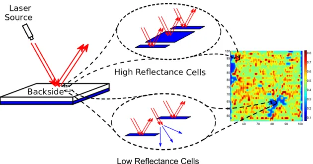
We propose a dramatically di↵erent approach to detect HTs inserted in IC chips during the fabrication phase. Metals in IC chips are strongly reflective to near-IR light, while silicon is transparent to light at those wavelengths. Backside optical imaging of the fabricated chip enables us to extract the full standard cell layout of the chip with the watermarks, which in turn can be validated to detect any modifications
to the IC layout (Figure 2·1). In addition to the original metal lines of standard cells, we also embed a maximal amount of metal in the M1 layer in the fill cells during the design stage to increase the total reflectance of the design to improve detection accuracy. This strong reflected pattern forms the signature of chip design which will be used for HT detection.
Figure 2·1: Backside Imaging of IC chips
Our optical measurements are highly modular and independent of the multitude of connections in the full IC chip. In addition, the physical principles behind the implementation of our watermarking scheme are also highly distinct from previous approaches. Although, like the first PUF (Pappu et al., 2002), it is an optical method that utilizes embedded scatters, their intended design and functionality are funda-mentally di↵erent. The scattering in (Pappu et al., 2002) was explicitly designed to be random and impossible to predict and replicate. In contrast, determinism is essen-tial to the functionality of our approach. We embed the watermark during the design phase and we can determine the optical response before fabrications. Our designed
signature must be predictable within our analytical range.
2.3.1 Optical Imaging Method
As the opaque metal layers prohibit front side imaging, backside imaging of inte-grated circuits is a well-established technique for failure analysis (Ippolito et al., 2004; Kindereit et al., 2007; K¨okl¨u and Unl¨u, 2010). Bright field images at near-infrared (IR) wavelengths (e.g. ⇠1 2µm) can be used for passive measurements for fault detection and localization, such as for inspecting the fidelity of the metal wires (Ip-polito et al., 2005). In addition to passive measurements, the active functionality of the circuit can also be probed via techniques such as thermal imaging (Ippolito et al., 2004), which records power dissipation via heat generation or laser-voltage imaging (LVI) (Kindereit et al., 2007), which records the switching response of the transistors. As integrated circuits shrink in size, a key challenge in these imaging techniques is to obtain sufficient spatial resolution to resolve each individual structure in each gate. The di↵raction limit imposes a fundamental restriction on the maximum spatial frequency that can be imaged using conventional optical systems which limits the resolution. The resolution of an optical system can be determined by the size of the impulse response of the system which takes the form of an Airy function (Novotny and Hecht, 2006), I(⇢)/ 2J1(2⇡⇢) 2⇡⇢ 2 (2.1) where ⇢ = N Ar/(M ) is the image space coordinate. The size of the impulse response is
x= 0.61
Here, is the wavelength of the light in free space and NA is the numerical aperture (NA =nsin✓) of the system, where n is the refractive index of the material in which the light propagates. J1 is Bessel Function of the First kind.
Due to their high NA capability (⇠ 3.4), complex solid immersion lenses provide a high resolution for fault analysis of integrated circuits (K¨okl¨u and Unl¨u, 2010). In this work, we can eliminate the need for the high resolution and can rapidly and accurately detect malicious tampering and the presence of an HT at relatively low NA’s (⇠0.8).
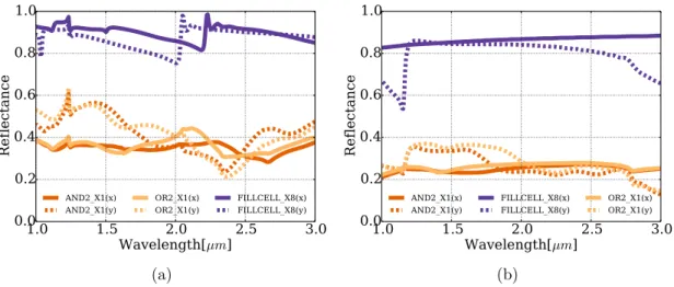
Our approach is based on the fact that for low NA’s in the near-IR, we can achieve impulse response functions with widths on the order of the gate size in 45nmor lower technology nodes (see Equation (2.2)). NA’s of 0.14, 0.42 and 0.5 correspond to spot sizes of approximately 4.6 µm, 1.5 µm and 1.3 µm, respectively at = 1.064µm. These correspond to common near-IR commercial objectives capable of imaging over 0.1 – 1mmfields of view (several thousand to half a million gates simultaneously). An image collected in this manner (i.e. at low NA, without a solid immersion lens) would, rather than resolve the detailed substructure of individual gate, produce a slowly varying image that tracks the average reflectance of each gate over its area. Although the individual gates are comprised of unique layouts of metal lines, Figure 2·2 shows that with both 15 nm and 45 nm technology, the responses of three di↵erent gates have distinctive signatures across the spectrum.
Figure 2·2 shows that fill cells which are engineered to contain maximum amount of metal, while meeting the metal density design rule constraints. These fill cells achieve distinguishable stronger response compared to common functional cells. We can leverage these stronger responses to strengthen the contrast of the response images in order to achieve higher HT detection rates.
(a) (b)
Figure 2·2: (a) The reflectance spectrum of functional gates and fill cells designed in 45 nm technology (computed via FDTD simulations). The response is computed for both X and Y polarizations of the illuminating field (solid and dashed lines, respectively). For X polarization, the incident electric field is polarized along the VDD and VSS rails. For Y polarization, the polarization is perpendicular. (b) The reflectance spectrum of functional gates and fill cells designed using 15nm technology. Fill cells still show much higher reflectance compared to functional cells.
on the standard cell layout. These patterns can serve as a robust, easily record-able optical watermark of IC chip. Any modifications through movement of cells or insertion of unwanted cells will result in a change in the watermark that can be measured with high fidelity. Imaging large fields of views provides the potential to perform these measurements on a large number of gates simultaneously. It also has the added benefit of considerably simplifying the required optical setup in comparison with commercial failure analysis tools. Our approach is a simple, rapid test to check for tampering of the IC chip at the fabrication stage. It utilize o↵-the-shelf tools to embed our engineered signature and it can be seamlessly integrated into typical IC fabrications.
2.3.2 Technology Scalability
While we demonstrate our approach at the 45 nm technology node level, we expect it to scale well to smaller technology nodes because our technique does not require high resolution imaging. We can estimate the efficacy of our proposed technique as gate sizes are reduced by considering the size of the impulse response of our optical system as described by Equation (2.2). The gate sizes reduction will limit our ability to detect a shift in the position or a change in the magnitudes of response of cells, and therefore the performance of our technique.
We can show that the reflectance di↵erence between di↵erent gates in optical imaging can be clearly distinguished. Case in point, in a 45 nm technology node (See Figure 2·2(a)), the reflectance di↵erence between AND gate and OR gate can be as much as 0.2, which is almost 50% of the total reflectance from AND2. Replacement of AND gate with an OR gate results in 50% change in reflectance variation. In contrast to the AND gate and OR gate, the reflectance of fill cells is as high as 90%. The distinguishable di↵erence between various gates scales in a 15nm technology node (See Figure 2·2(b)). The gates in 15nm technology node have smaller sizes, and also the reflectance of all the gate is weaker compared to gates in 45 nm technology node. The di↵erence between reflectance of di↵erent gates also scales with the technology nodes. However, the reflectance ratio between AND gate and OR gate still remains the same. Note that the AND gate is still around 50% of the reflectance of OR gate. By comparing the relative reflectance, we can detect the changes in the gate type. Moreover, in our method, the uniqueness of the image of a design is determined using the responses from individual gates and the neighboring e↵ects. The pixel size of our optical imaging method is 0.1µm2 while the smallest gate size of 45 nm technology node is 0.4⇥1µm2. This means that each gate can have multiple comparison points in HT detection. In our case, the minimum gate size of 45 nm technology is 0.26µm2,
which can contain as much as 30 data points. Even with 15nm technology, each gate can still have up to ⇠15 data points, which is sufficient for HT detection.
By applying interpolations on sampled points, our technique also scales well in modeling areas much larger than single gate. This enables measurements over a large field of view and therefore a large number of simultaneously imaged gates. Consid-ering an IC with ⇠ 1 B transistors, an average of 4 transistors per gate corresponds to approximately 250 M gates. For a gate size of 1.3µm2 corresponding to the 45 nm technology node, using a resolution of ⇡ 400 nm and MHz acquisition rates would mean that the whole chip would be imaged in a few minutes. This is a significant im-provement over the high NA imaging methods, where the sample is typically scanned with a scan size of 10⇠100nm as opposed to 400nm that we consider in this work.
2.3.3 Optical Simulation Methodology
FDTD computation for one gate area requires roughly half an hour computation time. The computational time grows exponentially with areas to simulate, i.e. a larger gate with area of 5 ⇠ 6 times of single gate takes 1 ⇠ 2 days to finish. Simulating the response for the whole layout of a typical 3 ⇠ 4 cm2 IC chip is computationally infeasible. Thus, in this work, we simulate each individual gate to construct a library of responses from near-IR excitement. The constructed response library determines the response of a given layout through simulations. Our method does not require the need for in-field measurements of “golden reference”. The FDTD method is widely used in modeling di↵erent microscopes, and it has been shown to work both analytically and experimentally (T¨or¨ok et al., 2008; C¸ apo˘glu et al., 2011).
In the previous work, we considered the FDTD simulations for each gate with periodic boundary conditions by simulating illumination on infinite tiling of the same gate (Zhou et al., 2015). With these boundary conditions, we simulate the response of each gate separately and obtain their optical response by calculating the reflected


![Table 2.2: Area of Inserted fill cells[µm 2 ], 0.19, 0.38, 0.57 represents the width of each fill cell in the array in [µm], 1, 2, 3, 4 represents number of rows and columns of the array.](https://thumb-us.123doks.com/thumbv2/123dok_us/9949356.2487684/67.918.339.636.113.226/table-area-inserted-cells-represents-represents-number-columns.webp)