Abstract A series of electromigration (EM) tests were performed as a function of temperature and current density to investigate lifetime statistics and damage evolution for Pb-free solder joints with Cu and Ni under-bump-metallizations (UBMs). The EM life-time was found to depend on the failure criterion used, so the results were compared based on the first resis-tance jump and conventional open-failure criterion. Solder joints with Cu UBM had a longer lifetime than Ni UBM based on the open-failure criterion, but the lifetime with Ni UBM became comparable when the first resistance jump criterion was applied. To deter-mine the temperature in solder joints, the Joule heating effect was investigated with experiments and finite element analysis. The temperature of solder joints was determined to be approximately 15C higher than that at the Si die surface when 1 A of current was applied. With the appropriate temperature correction, the activation energies and the current density exponents were found to be Q= 1.11 eV, n = 3.75 and Q= 0.86 eV, n = 2.1 based on the open-failure crite-rion for solder joints with Cu and Ni UBM, respec-tively. Based on the first resistance jump criterion, Q= 1.05 eV, n= 1.45 for Cu UBM andQ = 0.94 eV, n= 2.2 for Ni UBM, respectively. For solder joints with Cu UBM, voids were formed initially at the
Cu6Sn5/solder interface while the final open failure
occurred at the Cu3Sn/Cu6Sn5interface. For Ni UBM,
voids were formed initially at the Ni3Sn4/solder
inter-face leading to failure at the same interinter-face. The for-mation of intermetallic compounds (IMCs) was enhanced under current stressing, which followed lin-ear growth kinetics with time. The IMC growth was accompanied by volume shrinkage, which accelerated damage evolution under EM.
1 Introduction
With continuing demands to increase I/O density and power requirement, electromigration (EM) failure of solder joints raises increasing reliability concern for plastic flip-chip packages. It is anticipated that flip-chip solder joints will be subject to a current density in the order of 104A/cm2in the near future [1]. Although this current density level is still about two orders of mag-nitude lower than that for Cu interconnects, EM damage becomes a serious concern for solder joints due to their low current carrying capability [2]. In solder joints, the formation of intermetallic compounds (IMCs) at the interface between the solder and the under-bump-metallization (UBM) plays an important role in controlling EM reliability [2]. Noble or near-noble metals such as Cu or Ni in the UBM can diffuse rapidly in Pb or Sn by an interstitial diffusion mecha-nism [3–5], and react at a fast rate with Sn to form IMCs [6]. The implementation of eco-friendly Pb-free solders generates further interests in studying the effect of UBM on EM reliability of solder joints. This effect is expected to be more significant for Sn-based Pb-free S.-H. Chae (&)ÆX. ZhangÆK.-H. LuÆH.-L. ChaoÆ
P. S. Ho
Microelectronics Research Center, The University of Texas at Austin, Austin, Texas 78758-4445, USA
e-mail: [email protected]
M. DingÆP. SuÆT. UehlingÆL. N. Ramanathan Freescale Semiconductor, Technology Solution Organization, Austin, Texas 78735, USA DOI 10.1007/s10854-006-9026-2
Electromigration statistics and damage evolution for Pb-free
solder joints with Cu and Ni UBM in plastic flip-chip packages
Seung-Hyun ChaeÆXuefeng ZhangÆKuan-Hsun LuÆ Huang-Lin ChaoÆPaul S. HoÆ
Min DingÆPeng SuÆTrent UehlingÆ
Lakshmi N. Ramanathan
Published online: 22 September 2006
solders. Since Sn is a major constituent of the IMCs, its inexhaustible supply from the solder can greatly enhance the IMC formation to degrade EM reliability [6,7].
This study investigated the effect of UBM on EM reliability for Pb-free Sn-3.5Ag solder joints. The Cu UBM was compared with the Ni UBM. Due to the rapid reaction rate of Cu with Sn [7], the thick Cu stud in the UBM was of interest. For Ni UBM, the thin Ni film in the UBM was of primary interest due to the slower reaction rate of Ni with Sn [8]. Samples were tested under various temperature and current conditions to obtain EM statistical data. The EM lifetime was found to depend on the failure criterion used, so the results were compared based on the first resistance jump and conventional open-failure crite-rion. In accelerated solder EM tests, approximately 1 A current is usually applied [6, 7, 9], which can cause substantial Joule heating. Moreover, heat dis-sipation in plastic packages is much less efficient than in ceramic packages, so the Joule heating effect was taken into account to deduce EM statistics by com-bining experiments and simulation. EM damage evo-lution and failure mechanism were investigated by cross-sectional microscopy of solder joints, with emphasis on the morphology changes of solder joints with IMC growth.
2 Experimental
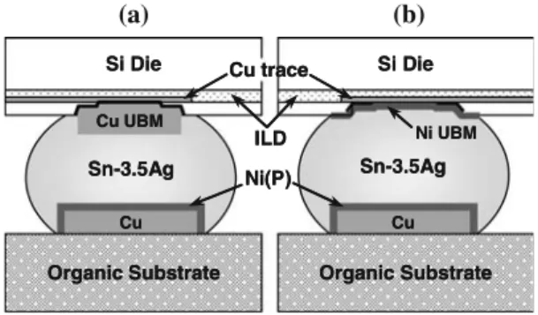
Figure1shows a schematic of the cross-sections of Sn-3.5Ag solder joints with two types of UBM in plastic packages. One had a 0.25lm-TiW/18lm-Cu UBM and the other a 0.1lm-Ti/2 lm-Ni UBM. Both Cu and Ni UBM were electroplated after sputter deposition of the seed layers. Thickness variations of Cu and Ni
UBM were ±4 lm and ±0.5lm, respectively. The passivation opening of the UBM was 50lm in diam-eter. On the substrate side, a 5 lm-Ni(P) was plated electrolessly on the Cu metallization. The Pb-free Sn-3.5Ag solder had a nominal diameter of 130 lm and a height of 80lm.
The resistance of a solder joint at room temperature was only a few mWwhereas that of entire circuitry of the test sample was ~1.1W. Thus it was difficult to detect the resistance change of a solder joint before it becomes significantly open [2]. To improve the sensi-tivity to track the resistance change, this study employed the Wheatstone bridge method. In one leg of the Wheatstone bridge circuit, two pairs of solder joints were connected in series, making the test structure a two-link (N= 2) system. Each pair served as one resistor unit of the bridge consisting of a cathode joint and an anode joint. Here, the cathode joint refers to a solder joint where electrons flowed from the substrate side to the die side, and the anode joint refers to one where electrons flowed in the opposite direction. The other leg consisted of a fixed and a variable resistor of the order of 103W. In this way, current flowed primarily through the solder joints. To start the EM test, the off-balance voltageVg
in the Wheatstone bridge circuit was set to zero by adjusting the variable resistor. The value of Vg was
directly correlated with net resistance changes of solder joints only. Thus the Vg traces enabled us to
detect the small resistance changes of solder joints with high sensitivity as damage developed. A detailed description of the Wheatstone bridge method can be found in Ref. [6].
In the EM test oven, a set of samples were arranged in a way that the Si backside of each sample was at-tached to a Cu plate in order to minimize temperature deviation of each sample and to facilitate Joule heat dissipation in the test sample. Thermocouples were sandwiched between the Si dies and the Cu plate to monitor the Si backside temperature, which was gen-erally higher than the oven temperature by 7–20C depending on the applied current.
To obtain statistical data, 12–15 samples (i.e. 24–30 pairs of solder joints) were tested in each run. The EM lifetime was measured at 115, 130, 140 and 150C with 1.01 A of current stressing. The current density dependence was extracted from experiments at 140C with 0.81, 1.01 and 1.11 A, corresponding to current densities of 4.12, 5.16 and 5.67 in units of 104A/cm2, respectively. Current density was calculated based on the area of the passivation opening, and all the above temperatures are referred to the surface temperature at the backside of the Si die.
Sn-3.5Ag Cu UBM Organic Substrate Cu Si Die Ni(P) Sn-3.5Ag Organic Substrate Cu Ni UBM Cu trace ILD Sn-3.5Ag Cu UBM Organic Substrate Cu Si Die Ni(P) Sn-3.5Ag Organic Substrate Cu Ni UBM (a) (b) ILD Cu trace Si DieSi eDi
Fig. 1 A schematic diagram of cross-sectioned Sn-3.5Ag solder
joints with (a) Cu under-bump-metallization (UBM), and (b) Ni UBM
3 Results and discussion 3.1 Failure criteria
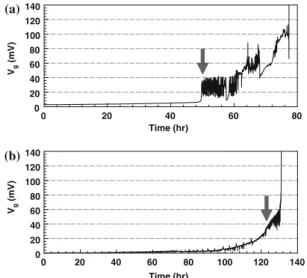
Figure2 represents typical Vg traces of solder joints
with Cu and Ni UBM. Initially, Vg increased slowly.
Then an abrupt jump in Vg occurred with
approxi-mately 30–40 mV change, which was followed by unstable fluctuations until the solder became electri-cally open. The Vg increase was more gradual in Ni
UBM than Cu UBM. The unstable fluctuations were attributed to simultaneous damage evolution and recovery process in the solder joint, which eventually led to an electrical open failure [10]. At this stage, a solder joint became unstable and vulnerable to failure. The period of unstable fluctuations lasted usually longer for solder joints with Cu UBM than with Ni UBM in this study, which could be related to their thickness difference. Numerical analysis showed that a 30–40 mV change in Vg corresponded to
approxi-mately 90–95 % opening of the solder joint, as shown in Fig.3. This was confirmed by cross-sectional SEM observation and will be discussed in Sect. 3.4. Based on these findings, the first resistance jump was suggested as an alternate failure criterion to supplement the conventional open-failure criterion to evaluate EM lifetime.
3.2 EM lifetime statistics
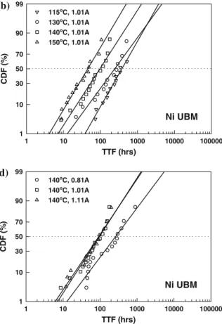
The cumulative distribution function (CDF) of solder joints with Cu and Ni UBM at various temperatures and currents are plotted in Figs.4and5. The results of
EM lifetime statistics are summarized in Table 1. Since each sample was a two-link structure (N= 2), CDF was deconvoluted based on the weakest link approximation to deduce the median-time-to-failure (MTTF) t50 for
single solder joints (N= 1) [11]. Based on the electrical open criterion, the lifetime of solder joints with Cu UBM was 1.5–4.0 times longer than that of solder joints with Ni UBM. In contrast, when the first resis-tance jump criterion was applied the lifetimes of solder joints with Cu and Ni UBM became comparable. This was attributed to the fact that the period of resistance fluctuation in Cu UBM solders amounted to 36–75% of the total lifetime whereas the period in Ni UBM sol-ders amounted to only 7–27%. Considering that the resistance fluctuation already corresponds to significant opening of a solder joint, it is important to select a proper failure criterion to evaluate solder reliability, particularly for a thick Cu UBM.
From the lifetime data the EM activation energy and the current density exponent for solder joints were calculated using the Black’s equation [12]:
t50¼Ajnexp Q kT
; ð1Þ
wheret50is the median-time-to-failure (MTTF),Ais a
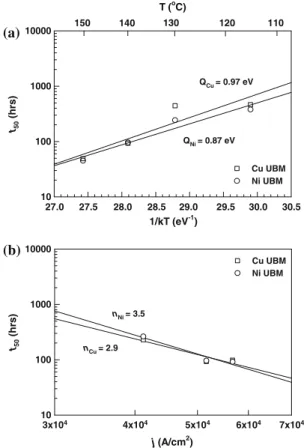
constant, jis the current density, nis the current den-sity exponent, Q is the activation energy, k is the Boltzmann constant, and Tis the temperature. Based on the open-failure criterion, activation energies of Sn-3.5Ag solder with Cu and Ni UBM were 1.03 and 0.80 eV, with current density exponents 5.1 and 3.3, respectively (Fig.6). In comparison, based on the first resistance jump criterion, the activation energies of the solder with Cu and Ni UBM were 0.97 and 0.87 eV (Fig. 7a), which are consistent with those from the open-failure criterion. However, the current density exponent was reduced significantly to 2.9 for the solder
Time (hr) 0 20 40 60 80 100 120 140 0 20 40 60 80 100 120 140 Time (hr) 0 20 40 60 80 Vg (mV) Vg (mV) 0 20 40 60 80 100 120 140 (a) (b)
Fig. 2 TypicalVgtraces of solder joints with (a) Cu
under-bump-metallization (UBM), and (b) Ni UBM. Arrows indicate where the first resistance jump criterion regards as failure
Ratio of voids 0.0 0.2 0.4 0.6 0.8 1.0 Vg (mV) 0 20 40 60 80 100
Fig. 3 Calculated off-balance voltageVgwith respect to the void
with Cu UBM while remaining about the same for the solder with Ni UBM (Fig.7b). This reflects that the resistance fluctuation period for solders with Cu UBM was substantially longer when the applied current was small. Thus the first resistance jump criterion resulted in more reduction of the EM lifetime at a lower current density. Nevertheless, the current density exponent for solder EM was in general higher than that for Cu interconnects, which is usually between 1 and 2 [13]. This suggests a significant amount of Joule heating during solder EM tests, which has to be properly taken into account to ensure reliable EM parameters.
3.3 Joule heating measurement and simulation
Due to the large applied current (~1 A), the Joule heating will increase the temperature of solder joints under current stressing, although the solder tempera-ture was often assumed to be the same as the tem-perature at the backside of a Si die [9, 14]. To determine the Joule heating effect, we measured resistance changes as a function of temperature and applied current, and supplemented the experimental results with finite element analysis (FEA). First, the
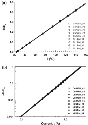
temperature coefficient of resistance (TCR) was determined by measuring the resistance with increas-ing temperature at a minimal applied current (50 mA). The TCR was found to be 3.6· 10–3(C)–1as shown in Fig.8a, which was between those for bulk Cu (3.9 ·10–3(C)–1) and 0.5lm wide Cu interconnects (3.3 ·10–3(C)–1) [15]. Next, the oven temperature was set to 120C, and resistance changes were mea-sured again with increasing applied current. The rela-tionship between the applied current and the resistance change was found to be DR/R0= 0.158·i2.165 from
Fig.8b. When the oven temperature was set to 140C the difference in the result was negligible. Combining this relationship with TCR, we found that the average temperature of the test structure was ~30C higher than the Si backside temperature at 1 A applied cur-rent.
To supplement the experimental results, the temperature distribution inside the test structure was calculated using FEA based on the dimensions and configurations of the current path including the sol-der joints, the Cu trace on the die side and the Cu trace in the substrate. The calculated average tem-perature in the test structure was force-fitted with the
TTF (hrs) 1 10 100 1000 10000 100000 CDF (% ) 1 10 30 50 70 90 99 115oC, 1.01A 130oC, 1.01A 140oC, 1.01A 150oC, 1.01A Cu UBM (a) TTF (hrs) 1 10 100 1000 10000 100000 CDF (% ) 1 10 30 50 70 90 99 115oC, 1.01A 130oC, 1.01A 140oC, 1.01A 150oC, 1.01A Ni UBM (b) TTF (hrs) 1 10 100 1000 10000 100000 CDF (% ) 1 10 30 50 70 90 99 140oC, 0.81A 140oC, 1.01A 140oC, 1.11A Cu UBM (c) TTF (hrs) 1 10 100 1000 10000 100000 CDF (% ) 1 10 30 50 70 90 99 140oC, 0.81A 140oC, 1.01A 140oC, 1.11A Ni UBM (d)
Fig. 4 (a)–(b) Temperature dependence, and (c)–(d) current density dependence of electromigration (EM) lifetime statistics of solder
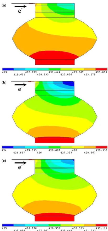
experimental result. At 0.81, 1.01 and 1.11 A of the applied current, the solder joint temperature turned out to be higher than that at the Si backside by 10, 15 and 17C, respectively (Fig.9). The primary source of Joule heating was the ~33 mm-long Cu trace in the substrate, which resulted in the temper-ature gradient in the solder as shown in Fig.9. Accordingly, the solder temperature in the substrate side was ~3C higher than that in the die side.
Correcting for the actual solder temperature, the activation energies and current density exponents were reanalyzed, and the refined results are summa-rized in Table2. The activation energies of EM were then in good agreement with the results obtained from Cu–Sn and Ni–Sn IMC growth in the literature [16–19]. The current density exponents were reduced considerably, although still higher than the typical value for Cu interconnects.
TTF (hrs) 1 10 100 1000 10000 100000 CDF (% ) 1 10 30 50 70 90 99 115oC, 1.01A 130oC, 1.01A 140oC, 1.01A 150oC, 1.01A Cu UBM (a) TTF (hrs) 1 10 100 1000 10000 100000 CDF (% ) 1 10 30 50 70 90 99 115oC, 1.01A 130oC, 1.01A 140oC, 1.01A 150oC, 1.01A Ni UBM (b) TTF (hrs) 1 10 100 1000 10000 100000 CDF (% ) 1 10 30 50 70 90 99 140oC, 0.81A 140oC, 1.01A 140oC, 1.11A Cu UBM (c) TTF (hrs) 1 10 100 1000 10000 100000 CDF (% ) 1 10 30 50 70 90 99 140oC, 0.81A 140oC, 1.01A 140oC, 1.11A Ni UBM (d)
Fig. 5 (a)–(b) Temperature dependence, and (c)–(d) current
density dependence of electromigration (EM) lifetime statistics of solder joints (N= 1) with Cu and Ni
under-bump-metalliza-tion (UBM), based on the first resistance jump criterion. (Note: TTF: Time to failure)
Table 1 Electromigration (EM) lifetime statistics of Pb-free Sn-3.5Ag solder joints with Cu and Ni under-bump-metallization (UBM)
based on two kinds of failure criteria at various test conditions Temperature* (C) Applied
current (A)
Current density (A/cm2)
Open-failure criterion First resistance jump criterion
Cu UBM Ni UBM Cu UBM Ni UBM
t50(h) r t50(h) r t50(h) r t50(h) r 115 1.01 5.16·104 1570 1.1 407 1.0 464 0.6 379 1.0 130 1.01 5.16·104 690 1.3 288 1.4 444 1.3 243 1.3 140 0.81 4.12·104 912 1.3 309 1.4 230 0.8 263 1.3 1.01 5.16·104 192 0.6 132 1.3 93 0.8 96 1.1 1.11 5.67·104 200 0.6 110 1.3 98 0.9 92 1.2 150 1.01 5.16·104 144 1.0 56 1.2 49 0.7 45 1.0
3.4 Failure analysis
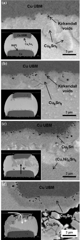
3.4.1 Damage evolution in solder joints with Cu UBM Due to the current crowding effect, EM failures were always observed in anode joints where electron flux flowed from the die side to the substrate side, consis-tent with those reported in other studies [6,7,9]. Fig-ure10b–d show morphological changes evolved in solder joints during EM test for 263 h at 140C (Si backside temperature). For comparison, a pristine solder joint in the as-received condition was included in Fig.10a. A small number of Kirkendall voids formed during solder reflow as can be seen between Cu UBM and Cu6Sn5. The Cu3Sn phase should be present
between Cu UBM and Cu6Sn5[20] although this layer
was too thin to be identified in Fig.10a.
Although fatal EM damages developed only in the anode joint (Fig.10d), some microstructural changes were observed in the joint without current stressing and in the cathode joint. Without current stressing (Fig. 10b), the number of Kirkendall voids increased in solder and the scallop-shaped Cu6Sn5 phase became
flattened during thermal aging. This is because Cu is the dominant diffusing species and the valleys in the scallop-shaped Cu6Sn5 phase are the faster diffusion
paths for Cu atoms [20]. The increase of voids and flattening process progressed further with longer aging time and increasing temperature.
When an electric current was applied, additional microstructural changes were observed. In the cathode joint (Fig.10c), (Cu,Ni)6Sn5 migrated from the
sub-strate side to the die side, where Cu atoms migrated from the initial (Cu,Ni)6Sn5phase formed on the Ni(P)
1/kT (eV-1) 27.0 27.5 28.0 28.5 29.0 29.5 30.0 30.5 T (o C) t50 (hrs) 10 100 1000 10000 Cu UBM Ni UBM QCu = 1.03 eV QNi = 0.80 eV 110 150 140 130 120 (a) j (A/cm2) 3x10⁴ 4x10⁴ 5x10⁴ 6x10⁴ 7x10⁴ t50 (hrs ) 10 100 1000 10000 Cu UBM Ni UBM nCu = 5.1 nNi = 3.3 (b)
Fig. 6 (a) Activation energy, Q, and (b) current density
exponent,n, deduced from the open-failure criterion
1/kT (eV-1) 27.0 27.5 28.0 28.5 29.0 29.5 30.0 30.5 T (oC) t50 (h rs ) 10 100 1000 10000 Cu UBM Ni UBM QCu = 0.97 eV QNi = 0.87 eV 110 150 140 130 120 (a) j (A/cm2) 3x10⁴ 4x10⁴ 5x10⁴ 6x10⁴ 7x10⁴ t50 (hrs ) 10 100 1000 10000 Cu UBM Ni UBM nCu = 2.9 nNi = 3.5 (b)
Fig. 7 (a) Activation energy, Q, and (b) current density
exponent,n, deduced from the first resistance jump criterion
Table 2 Reanalyzed
activation energies and current density exponents based on finite element analysis for solder temperature
Open-failure criterion First resistance jump criterion
Cu UBM Ni UBM Cu UBM Ni UBM
Activation energy (eV) 1.11 0.86 1.05 0.94
substrate finish layer during solder reflow, and Ni atoms migrated from both the (Cu,Ni)6Sn5phase and
the substrate finish layer. The Ni concentration de-creased with distance from the Ni finish layer to the IMC. Meanwhile, at the Cu UBM/Cu6Sn5 interface,
the Cu3Sn layer grew thicker under current stressing.
The density of Kirkendall voids also increased but the density difference with and without current stressing was not so clear. At this point, most of the Kirkendall voids still located in the Cu3Sn layer near the UBM/
Cu3Sn interface while the Cu UBM continued to be
depleted as shown in Fig.10c. This indicates that Sn atoms were driven by current through the IMC layers to react with Cu atoms while Cu atoms diffused into solder in the direction opposite to the electron flow. Without Sn diffusion, the additional depletion of Cu UBM cannot be explained as compared with the case without current stressing (Fig.10b). Without Cu dif-fusion, Kirkendall voids would have moved toward the substrate side away from the Cu UBM/Cu3Sn
inter-face. Thus both Cu and Sn atoms interdiffused in the cathode joint, but the diffusion of Cu atoms might be somewhat suppressed due to the electron wind force.
At the anode joint (Fig.10d), a significant amount of IMC formation and damage evolution was
observed. Most of the Cu UBM was dissolved into solder to form IMCs. A large domain of Cu6Sn5,
enhanced by the electron flow, was formed to de-velop an extended morphology in concert with the electron flux. In contrast, the Cu3Sn layer maintained
its parallel interfaces, i.e. the Cu UBM/Cu3Sn
inter-face and the Cu3Sn/Cu6Sn5 interface were almost
parallel to each other during Cu3Sn growth as shown
in Fig.10d. The amount and location of Kirkendall voids in the anode joint were similar to those in the cathode joint. Interestingly, the Kirkendall voids formed during solder reflow had very little to do with EM-induced voids or failure even in the anode joint as shown in Fig.10d. However, the formation of Kirkendall voids during thermal aging or under current stressing can raise other reliability concerns since they weaken the mechanical strength of solder joints [20].
Figure 11 displays EM damage evolution in the anode joint with Cu UBM. At an early stage, IMC layers grew by consuming Cu UBM (Fig.11a). TheVg
increase was negligible in this stage. Next, EM-in-duced voids were initiated at the Cu6Sn5/solder
inter-face as shown in Fig.11b. These voids grew independent of Kirkendall voids in the Cu3Sn layer
observed after solder reflow. At this point,Vgwas still
only a few mV but increased gradually, corresponding to an increase of several mW in resistance [10]. The current crowding effect on UBM consumption and void initiation was weak due to the thick Cu UBM structure. Figure 11c depicts a solder joint after an abrupt jump to ~40 mV in Vg. At this point,
sub-stantial Cu6Sn5 growth was observed, and EM voids
were embedded in the Cu6Sn5 layer near the Cu3Sn/
Cu6Sn5 interface. Before discrete voids were
con-nected to each other (Fig.11b), the region between voids had a high current density, which further en-hanced Cu6Sn5 growth with simultaneous void
propa-gation. The resistance increased abruptly when the discrete voids became connected to form a global crack, which could be driven by tensile stress devel-oped during IMC formation. Note that the solder joint was almost open at this stage as was expected based on the result obtained in Fig.3. At this stage, Cu6Sn5
grew preferentially through the region where solder was still connected. When an open failure finally oc-curred, an extensive formation of Cu6Sn5 was
ob-served connecting the IMC on the die side with that on the substrate side as shown in Fig. 11d. The void size increased further while the Cu3Sn layer grew but at a
lower growth rate compared with Cu6Sn5. This
even-tually led to crack that propagated through the Cu6Sn5
phase near the Cu3Sn/Cu6Sn5interface.
Current, i(A) 0.1 ∆ R/R 0 0.001 0.01 0.1 1 Cu UBM_#1 Cu UBM_#2 Cu UBM_#3 Cu UBM_#4 Cu UBM_#5 Ni UBM_#1 Ni UBM_#2 Ni UBM_#3 Ni UBM_#4 T (o C) 20 40 60 80 100 120 140 160 R/R r 1.0 1.1 1.2 1.3 1.4 1.5 Cu UBM_#1 Cu UBM_#2 Cu UBM_#3 Cu UBM_#4 Cu UBM_#5 Ni UBM_#1 Ni UBM_#2 Ni UBM_#3 Ni UBM_#4 (a) (b) 1.0
Fig. 8 (a) Plot of R/Rrwith temperature for the temperature
coefficient of resistance (TCR) measurement, and (b) plot of the resistance increase with current
3.4.2 Damage evolution in solder joints with Ni UBM Figure12 shows the morphology of cross-sectioned solder joints with Ni UBM after 150 h of an EM test at
130C (Si backside temperature) with 1.01 A. A thin Ni3Sn4 layer had been formed between the Ni UBM
and the solder during solder reflow, but little change occurred in the solder without current stressing
Fig. 9 Simulated
temperature (inK) of the anode solder joint under current stressing of (a) 0.81 A, (b) 1.01 A, and (c) 1.11 A. Top: die side; bottom: substrate side
Fig. 10 SEM micrographs of (a) the joint with Cu under-bump-metallization (UBM) in a pristine sample, (b) the joint without current stressing at 140C for 263 h, (c) and (d) the cathode joint and the anode joint from the same sample in (b) with 1.01 A current stressing
Fig. 11 Electromigration (EM) damage evolution in the anode
joint with Cu under-bump-metallization (UBM). (a) Initial stage of Cu depletion, (b) void initiation prior to the resistance jump, (c) crack propagation subsequent to the resistance jump, and (d) final open failure
(Fig.12a). In the cathode joint (Fig.12b), Ni atoms from the substrate finish layer migrated toward the die side to form Ni3Sn4to sustain the growth of Ni3Sn4on
the die side. In contrast, Ni3Sn4growth on the substrate
side was enhanced at the beginning but subsequently retarded as Ni in the substrate finish layer was de-pleted. When Ni was sufficiently depleted, needle-like fissures were found in the Ni(P) finish layer as shown in Fig.12b. This indicates the migration of Ni instead of Sn during solid state reaction although Chen et al. considered Sn to be the dominant diffusing species in the reaction couple with Ni sandwiched in-between Sn-based solder [21]. In the anode joint (Fig.12c), EM-induced voids formed at the Ni3Sn4/solder interface as
a result of enhanced growth of Ni3Sn4 by the current
flow. The growth of Ni3Sn4 was slower than Cu6Sn5,
resulting in a slower dissolution of Ni UBM than that of Cu UBM.
Damage evolution in the anode joint with Ni UBM is depicted in Fig. 13. At an early stage where the change inVgwas negligible, initial voids formed at the
current crowding region as shown in Fig. 13a. Some part of Ni UBM was dissolved into solder to form Ni3Sn4. Continuing test led to the growth of voids,
which propagated through the Ni3Sn4/solder interface
(Fig. 13b). At this point, the IMC growth was not substantial with a relatively small volume of void for-mation. Although voids occupied over a half of the interface, Vgwas only a few mV. Compared with Cu
Fig. 12 SEM micrographs of (a) the joint with Ni
under-bump-metallization (UBM) without current stressing at 130C for 150 h, and (b) and (c) the cathode joint and the anode joint from
the same sample in (a) with 1.01 A current stressing Fig. 13joint with Ni under-bump-metallization (UBM). (Electromigration (EM) damage evolution in the anode a) Ni depletion and void initiation, (b) void propagation along intermetallic compound (IMC)/solder interface, (c) further IMC and void growth, and (d) nearly open
UBM, Ni UBM showed more regular void growth through the Ni3Sn4/solder interface, which may
ac-count for the more gradual increase of Vg as seen in
Fig. 2. Further void growth increased local current
density, leading to accelerated IMC and void growth. In Fig.13c, the amount of Ni3Sn4increased in the
re-gion where solder was still connected while voids be-came much larger. This stage corresponded to~10 mV of Vgwhere voids occupied nearly 70% of the IMC/
solder interface. Figure13d shows the EM damage state of a solder joint when unstable resistance fluctu-ation occurred. At this stage, the solder joint became almost open with a large amount of IMC accumulated on the substrate side. A number of solder joints were melted after this stage due to the increase in Joule heating prior to the final open failure.
3.5 IMC growth rate
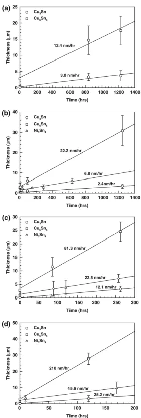
Volume change due to IMC formation generated stress within a solder joint. When Cu and Ni atoms react with Sn atoms to form Cu3Sn, Cu6Sn5 and Ni3Sn4, the
overall atomic volumes decrease by 7.7, 5.1 and 11.4%, respectively. This induces a tensile stress within the solder joint, which can further degrade EM reliability when combined with void formation due to current enhanced IMC formation. Figure14 plots nominal thickness of each IMC in anode joints as a function of time and temperature. The nominal thickness was calculated by dividing the cross-sectional area of each IMC with the original width of the corresponding UBM. Areas of IMC in both the die side and the substrate side were added since independently grown Cu6Sn5from each side would finally connect as shown
in Fig.11d. Current enhanced IMC growth followed linear growth kinetics as shown in Fig.14. The growth kinetics of IMC without current stressing had been reported to follow a t1/2 or t1/3 dependence [17, 19]. With the passage of an electric current, Gan et al. re-ported parabolic growth kinetics for IMC growth [22], although the time dependency was not reported in another study [21]. Recently we have formulated a kinetic model verifying the linear growth of IMCs when an EM driving force dominates the chemical interdiffusion [23]. In this study, the IMC growth rate was found to follow the order of Cu6Sn5> Ni3Sn4>
-Cu3Sn. Because Cu6Sn5grew several times faster than
the other two IMCs, the overall tensile stress caused by the formation of a large amount of Cu6Sn5 could be
significant although its molar volume change is the smallest of three IMCs. In contrast, relatively small amount of Ni3Sn4formation would have a large effect
on EM damage since both the accompanying molar volume shrinkage and its Young’s modulus (133.3 GPa) [24] are the largest of the three IMCs. Continuous growth of IMCs as enhanced by electric current increased the tensile stress with time, leading to Time (hrs) 0 50 100 150 200 Thi ckness ( µ m) 0 10 20 30 40 50 Cu3Sn Cu6Sn5 Ni3Sn4 210 nm/hr 25.2 nm/hr 45.6 nm/hr Time (hrs) 100 50 0 150 200 250 300 Thi ckness ( µ m) 0 5 10 15 20 25 30 Cu3Sn Cu6Sn5 Ni3Sn4 81.3 nm/hr 12.1 nm/hr 22.5 nm/hr Time (hrs) 0 200 400 600 800 1000 1200 1400 0 200 400 600 800 1000 1200 1400 Thi ckness ( µ m) 0 10 20 30 40 Cu3Sn Cu6Sn5 Ni3Sn4 22.2 nm/hr 2.4nm/hr 6.8 nm/hr Time (hrs) Thi ckness ( µ m) 0 5 10 15 20 25 Cu3Sn Cu6Sn5 3.0 nm/hr 12.4 nm/hr (a) (c) (b) (d)
Fig. 14 Nominal intermetallic compound (IMC) thickness with
respect to time under 1.01 A current stressing at (a) 115C, (b) 130C, (c) 140C, and (d) 150C of the Si backside temperature
significant driving force for crack propagation. Thus IMC growth is one of the key factors controlling EM reliability of Pb-free solder joints.
4 Summary
EM studies were conducted on Pb-free Sn-3.5Ag sol-der joints with Cu and Ni UBM in plastic flip-chip packages. Si backside temperatures of 115, 130, 140 and 150C were chosen for tests with 1.01 A current stressing. Two more tests at 140C were performed with 0.81 and 1.11 A in order to determine the current density exponent. To supplement the open-failure cri-terion, a first resistance jump failure criterion was used to analyze EM lifetime results. Solder joints with thick Cu UBM had a longer lifetime than those with thin Ni UBM, based on the open-failure criterion; however, lifetime of Ni UBM solders was comparable if the first resistance jump criterion was applied. This was due to the longer resistance fluctuation period of solder joints with thick Cu UBM. Numerical analysis of Vg and
failure analysis showed that solder was almost open at the onset of unstable resistance fluctuations. Experi-ments and finite element analysis were conducted to determine the Joule heating effect and found the sol-der temperature to be 10, 15 and 17C higher than the Si backside temperature at 0.81, 1.01 and 1.11 A. Taking this into account, we obtainedQCu = 1.11 eV,
nCu= 3.75 and QNi= 0.86 eV, nNi= 2.1 based on the
open-failure criterion. The correction for the Joule heating effect resulted in a reduction of the current density exponents. In solder joints with Cu UBM, EM voids were found to initiate at the Cu6Sn5/solder
interface but voids for final failure moved near the Cu3Sn/Cu6Sn5 interface. IMCs grew actively as voids
grew. The EM-induced voids evolved independently of the initial Kirkendall voids in the Cu3Sn layer. In
sol-der joints with Ni UBM, the final failure was observed at the Ni3Sn4/solder interface where voids initially
formed. EM damage evolution was expected to be accelerated with IMC growth, which would induce significant tensile stresses due to decrease in the overall atomic volume. The enhanced IMC growth under current stressing followed linear kinetics with time and
played an important role in controlling EM reliability of Pb-free solder joints.
Acknowledgements This work was supported in part by the
Semiconductor Research Corporation and the technical support provided by Freescale Semiconductor Inc. is gratefully acknowledged.
References
1. M. Ding, H. Matsuhashi, G. Wang, P.S. Ho, inProceedings of IEEE 54th Electronic Components and Technology
Con-ference(Las Vegas, NV, 2004), p. 968
2. K.N. Tu, J. Appl. Phys.94, 5451 (2003)
3. B.F. Dyson, T. Anthony, D. Turn bull, J. Appl. Phys.37, 2370 (1966)
4. W.K. Warburton, D. Turnbull, inDiffusion in Solids, eds. by A.S. Nowick, J.J. Burton (Academic, New York, 1975), pp. 171–226
5. D.L. Decker, C.T. Candland, H.B. Vanfleet, Phys. Rev. B11, 4885 (1975)
6. M. Ding, G. Wang, B. Chao, P.S. Ho, inProceedings of IEEE 43rd Annual International Reliability Physics Symposium
(San Jose, CA, April 2005), p. 518
7. Y.C. Hu, Y.H. Lin, C.R. Kao, K.N. Tu, J. Mater. Res.18, 2544 (2003)
8. J.W. Jang, D.R. Frear, T.Y. Lee, K.N. Tu, J. Appl. Phys.88, 6359 (2000)
9. J.W. Nah, J.O. Suh, K.N. Tu, J. Appl. Phys.98, 013715 (2005) 10. M. Ding, G. Wang, P.S. Ho, Appl. Phys. Lett. (Submitted) 11. M. Gall, PhD Dissertation (The University of Texas at
Austin, 1999)
12. J.R. Black, inProceedings of IEEE 6th Annual International
Reliability Physics Symposium (Los Angeles, CA, 1967),
p. 148
13. A.S. Oates, Appl. Phys. Lett.66, 20 (1995)
14. Y.H. Lin, C.M. Tsai, Y.C. Hu, Y.L. Lin, C.R. Kao, J. Elec-tron. Mater.34, 27 (2005)
15. K.-D. Lee, PhD Dissertation (The University of Texas at Austin, 2003), pp. 33–34
16. Y.C. Chan, A.C.K. So, J.K.L. Lai, Mat. Sci. Eng. B 55, 5 (1998)
17. J.-W. Yoon, S.-B. Jung, J. Alloys Compd.359, 202 (2003) 18. C.N. Liao, C.T. Wei, J. Electron. Mater.331137 (2004) 19. Z. Chen, M. He, G. Qi, J. Electron. Mater.33, 1465 (2004) 20. K. Zeng, R. Stierman, T.-C. Chiu, D. Edwards, K. Ano, K.N.
Tu, J. Appl. Phys.97, 024508 (2005)
21. C.-M. Chen, S.-W. Chen, J. Appl. Phys.90, 1208 (2001) 22. H. Gan, K.N. Tu, J. Appl. Phys.97, 063514 (2005)
23. H.-L. Chao, S.-H. Chae, X. Zhang, K.-H. Lu, J. Im, P.S. Ho,
inProceedings of IEEE 44th Annual International Reliability
Physics Symposium(San Jose, CA, March 2006), p. 250
24. D.R. Frear, S.N. Burchett, H.S. Morgan, J.H. Lau (eds.), in
The Mechanics of Solder Alloy Interconnects(Van Nostrand