A CUSTOMIZABLE SoPC ARCHITECTURE FOR GA BASED
ON COMPLETE HARDWARE EVOLUTION
1A. SWARNALATHA, 2A.P. SHANTHI
1Dept. of Electronics and Communication Engineering,
St. Joseph’s College of Engineering, Anna University, Chennai, India. 2
Dept. of Computer Science and Engineering, Anna University, Chennai, India.
E-mail: [email protected] , [email protected]
ABSTRACT
A Genetic Algorithm (GA) is a computer based search optimization technique that uses the Darwinian “Theory of Evolution” as a model for finding exact and approximate solutions. GAs belong to a large family of heuristic algorithms called Evolutionary algorithms (EA) which are being increasingly utilized for solving complex optimization and search problems. The large computation time consumed by a GA implemented in software makes it unsuitable for real time applications. This hurdle is overcome by shifting the implementation to hardware, which drastically speeds up the time factor, thus presenting a scope for real time applications. Major issues to be addressed in hardware implementation are silicon utilization, scalability, providing flexibility and reduced computational delays. This work presents a customizable Complete Hardware Evolution (CHE) based GA architecture. Along with the generic modules for the genetic operators of the GA, modules named Flush and Replace Memory (FRM), Memory Module (MM), and a sorting module form the main components of this architecture. These modules can facilitate System on Programmable Chip (SoPC) implementation for different applications of GA. The coding is done using Verilog Hardware Description Language (HDL) and simulated using Xilinx ISE 9.1i simulator. Each module is separately simulated and synthesized for a Commercial Off The Shelf (COTS) Field Programmable Gate Array (FPGA). The resource utilization and the critical path delay of the modules are evaluated and presented for Xilinx Virtex – 4 FPGA.
Keywords: Genetic Algorithm, Complete Hardware Evolution, FPGA, Sopc, Computational Delay,
Resource Utilization..
1. INTRODUCTION
Genetic Algorithms (GAs) are adaptive methods which are used to solve a variety of search and optimisation problems. They are based on the genetic processes of biological organisms [1, 2]. Over many generations, natural populations are said to have evolved according to the principles of natural election and “survival of the fittest”, first clearly stated by Charles Darwin in “The Origin of Species” [3]. By mimicking this process, genetic algorithms are able to evolve solutions to real world problems, if they have been suitably encoded. GAs are used to design bridge structures, for maximum strength/weight ratio, or to determine the least wasteful layout for cutting shapes from cloth, or to schedule and organise a managerial problem. They are also be used for online process control, such as in a chemical plant, or load balancing on a multi-processor computer system, for design of layout on
PCB, design of electronic systems, communication networks, scheduling and resource allocation, in robotics for trajectory planning, neural networks, design of adaptive filters in signal processing, in combinatorial optimization for set covering, travelling salesman, routing, bin packing, graph colouring and partitioning. Having such a varied domain of applications, it still has not attained a remarkable edge in real time implementations. It is mostly applied in an off – line manner. This is because of the huge computation time involved in the process of evolution [4].
Software accommodates this change quiet easily but hardware based systems are not flexible. Changes are very difficult once designed and fabricated. However, a general purpose GA engine requires certain parts of its design to be easily configurable. Thus hardware based GA applications were not feasible until the advent of reconfigurable devices. The motivation for implementing a GA in hardware stems from the fact that they are very much CPU intensive, while also being intrinsically parallel algorithms. The basic operations of a GA can be executed in a pipelined fashion, which could also be replicated for different members of the population [6]. An added advantage with hardware implementation is the elimination of the need for complex time and resource consuming protocols needed by an equivalent software implementation to interface with the main application [7]. So hardware implementation is presented as a solution to overcome this hurdle of huge computation times and increase the viability of these algorithms.
By shifting the implementation to hardware, a scope for real time applications is presented, as drastic speed - up in terms of computation time is now possible. Hence, it follows that a hardware implementation of GA would be appreciable for problems too complex for software. The first hardware based GA using Field Programmable Gate Arrays (FPGAs) was presented by Scott et.al, in 1995 [4].Evolutionary techniques have made use of unconventional properties of the physical device, yielding designs that defy conventional analysis [8]. It is this unrestricted model that interests all researchers. FPGA implementation combines the speed and massive parallelism of hardware with the flexibility of software. They are conducive to computational modeling and allow a vast number of configurations that compute different functions [9]. This has paved a path for GA to be applied to real time applications through a hardware implemented GA. But hardware evolution has several aspects that need not be addressed in software evolution, like scalability, flexibility, transient effects, feedback loops, propagation delays, signal loss, power dissipation, etc. The presented work is a generic architecture whose modules can be customized to suit different applications. They have been synthesized for the Xilinx Virtex – 4 Commercial Off The Shelf (COTS) FPGA. The modules performing the genetic operators are portable as they are available as a net list of gates after synthesis.
2. RELATED WORK
D. Scott et al. [4] in 1995 presented the first working implementation of a hardware based genetic algorithm. The board consisted of eight FPGA’s, shared memory and a PC on which the genetic algorithm was run. The HGA was designed with parameterized modules to allow scalability, providing easy implementation. Pipelining and parallelism were employed to achieve improvement in speed. The selection module was parallelized and the selection-crossover-fitness modules were replicated to achieve speed – ups in the pipelined structure. A simple crossover operator and selection algorithm was designed. The benefits of hardware were combined with the benefits of software GA for the first time.
Gunnar Tufte et al. [10] in 1999 proposed a new approach to evolvable hardware called Complete Hardware Evolution (CHE). The main feature of that implementation was that a hardware pipeline for the genetic evolution process was achieved. Control hardware was created for communication between the PC and the external boards. The problem of memory handling was solved by using LogiBlock from Xilinx Foundation Series. This CAD tool automatically generated the storage modules. A 4 x 1 multiplexor based on functional evolution was tested and validated.
Shruthi Narayanan et al [11] developed modules to implement a GA in Verilog and VHDL in compatibility with the MATLAB tool box. Simulations for two fitness functions were presented and compared with the Genetic Algorithm Optimization Toolbox (GAOT).
Michalis Vavouras et al. [6] implemented an improved version of the HGA known as parameterized HGA (P-HGAv1) on the XUPV2P platform where the depth of the shared memory was increased to support large population sizes. In order to create a flexible and low cost design, the embedded Power PC of this FPGA as well as special-purpose cores like multipliers from the Xilinx Core Generator were utilized. The block RAM on the board was used for memory. To the first implemented architecture [2], a new module was added, the fitness evaluation module, which consisted of built-in multiplier blocks and adders, a controller and a multiplexer. The multipliers were implemented in a pipeline manner.
Pradeep R. Fernando et al. [7] presented a customizable FPGA core of a general purpose GA engine. The core was presented as a gate - level net list which could be tailored to suit the user’s requirement. Also, additional hardware resources like Power PC and external Block RAM were utilized. Fitness evaluation module was replaced by a look – up table which consisted of the required results for the different chromosomes. The block memory was used to store the lookup based fitness evaluation module. Hardware implementation of this soft core was able to achieve the global optima, or within 3.7% of the global optima.
Swarnalatha and Shanthi [13] had presented a CHE based architecture which was designed for optimisation of single variable functions. Three functions were used to test the ability of the architecture to optimize. The fitness evaluation module was required to evaluate the optimum value of the single variable to suit the function under consideration. The design used five modules along with one memory module, totally constructed on the Configurable Logic Block (CLB) logic of the FPGA. Resource utilization for the different functions implemented varied from 0% - 94% approximately. This architecture was proposed as an application specific system. The same architecture would not support other real world applications because of the following hurdles.
• Limitation on the number of generations through which that architecture could traverse.
• The exhaustive usage of the limited number of available I/O blocks.
These limitations have been overcome in the present work by enhancing the architecture by
adding some extra modules called Flush and Replace Memory (FRM) which incorporates elitism in its operation and a sorting module (Figure.1). These modifications result in a customizable framework which is generic and hence can be adapted to suit any application. In contrast, to all the reported hardware systems which use external hardware / software support like Power PC, Nios processor or use boards with multiple FPGAs with interfaced external memory, the present framework implements the different operations of the GA, i.e. chromosome generation, selection, crossover, mutation and storage, all on a single FPGA, leading to a SoPC implementation. The design issues related to the proposed architecture are presented in the next section.
3. DESIGN ISSUES
The literature shows that hardware based GA systems are being developed in various styles for different application. The contribution of this paper is focused towards developing a complete SoPC architecture for implementing GA, on just a single COTS FPGA.
Behavioral modeling of the complete framework is done using the Hardware Description Language (HDL), Verilog. Synthesis and simulation of the HDL code is executed using Xilinx ISE 9.1i simulator [14]. Every module is indigenously modeled and implemented on the CLB of a single off-the-shelf FPGA. The designed architecture aims to achieve the following criteria in hardware.
• The flexibility that is inherently available with software
• A customizable generic framework • Achieving scalability with respect to
logic slices and I/O blocks
• Achieving significant reduction in computational delay, leading to a drastic speed – up
Since the code is in HDL, such variations can be incorporated into the design.
In hardware structures memory access is a critical bottleneck with respect to speed of computation. High computational speed is a requirement of this architecture. Thus, the memory is also built into the FPGA itself. With such population based algorithms as the GA, this would result in high silicon utilization hindering the creation of SoPC. This hurdle is explicitly established through the presented results of Table 1. The synthesis results of Table.1. are for a scaled up application of GA wherein the length of the chromosome would run to a few hundred bits using the architecture presented in [13]. The tabulated results show that with each generational run the resource utilization is linearly increasing and the device utilization ratio is exceeding 100%. This indicates that the chip does not support generational runs of the order of just 9 runs when the chromosome length is increased. The linear increase is witnessed for both logic utilization and I/O blocks. It is this limitation that is being handled in the proposed architecture.
In the enhanced framework presented, some extra behavior based modules are incorporated. These are named as Flush and Replace Memory (FRM) and Sorting - a module for sorting the contents of the memory. The FRM incorporates the elitism property of the genetic algorithm. With this modification, the memory size does not linearly grow with scaling in the number of generations and also supports scalability. The memory requirement remains the same as that of the initial population, for every generational run. Hence, a huge conservation in resource utilization is achieved enabling SoPC characteristics for the proposed architecture. The results and the operational flow of these blocks are presented in the next section.
4. THE PROPOSED SOPC ARCHITECTURE
FORGA
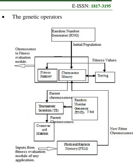
The proposed architecture consists of six main modules, which could be built as a SoPC on any COTS FPGA. The required memory module is also placed within the CLBs of the FPGA. The results obtained are presented in this section. Figure 1 shows the block diagram of the proposed system. The process can be divided into three levels viz,
• The generation of the initial population • The memory handling section
[image:4.612.328.559.71.363.2]• The genetic operators
Figure. 1 Block Schematic of the Proposed Architecture.
4.1 The generation of the initial population
4.2 The Memory Section
This section comprises of a memory module and a module for sorting its contents in the descending order of fitness values. The FRM module is also developed in conjunction with this section of the architecture.
• Memory Module (MM): The memory
module consists of two separate memories, one for the chromosomes (Chromosome Memory) and the other for the storage of their fitness values (Fitness Memory). The initial population of randomly generated chromosomes is stored in the chromosome memory. Since memory is also on – chip, this can be accessed at full clock speed thus eliminating the crisis of slow memory access. But, this accommodation would occupy significant physical area. Thus, the area overhead or silicon utilization on the FPGA is scaled up but computational speeds get drastically reduced. The memory is a collection of 2 – D resisters which can be indexed as per requirement. Now the individual chromosomes may be passed to the fitness evaluation module for fitness calculation.
• Sorting Module (SRM): After the
evaluation of fitness, for the chromosomes of the whole population, the chromosomes and their corresponding fitness values are arranged in descending order of their fitness by the sorting block in the MM. This is required for flushing out the least fit chromosomes to accommodate better child chromosomes.
• Flush and Replace Module (FRM): This
module incorporates elitism into the system. This block is mainly responsible for the slice logic conservation advantage of this CHE implementation. This checks and compares the two least fit genomes of the population with the two child genomes newly generated. If the fitness of the new genomes is better than the existing genomes of the population, then the generated genomes flush out the weakest two genomes and occupy their position in the population. The corresponding fitness values are also suitably substituted. The resulting new population is now called, the next generation, over which the iterative process of evolution continues. Thus the best chromosomes are retained in the population and the weaker are made better.
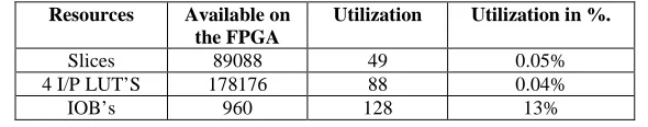
These modules are modeled and synthesized for a population size of 32 chromosomes, on a Virtex – 4 FPGA (XC4VLX200). The resources utilization for this level is presented in Table.3. The critical path delay of this module is achieved as 4.317ns.
4.3 The genetic operators
The genetic operators viz, selection, crossover and mutation can be implemented in accordance to the application under consideration. There are a huge number of variants which are available in literature. The choice of operators would depend on the application. Any specific choice of selection, crossover and mutation can be designed and attached to this framework. Since the population size here is 32 a 5 bit (25 = 32) RNG is used to randomly select two pairs of parent chromosomes for crossover. The selection method used here is tournament selection and the crossover is single point crossover. The process involved in this level is enumerated here. These can be used for any application but needs to be customized as per specifications of the problem at hand.
• RNG: 5 bit: The five bit RNG generates
two random numbers these numbers are used to index to the chromosome memory and the corresponding two chromosomes can be chosen to be operated on, by the selection module.
• Tournament Selection (TS): The
selection module selects two chromosomes as parents for recombination based on the indexing provided by the 5 – bit RNG. The highest fit chromosome out of the two chromosomes selected as probable parents, is chosen as one of the parent. The selection of both the parents is executed in this manner. In TS, every chromosome has an equal probability of being chosen as a parent. Thus, even the weak chromosomes have a chance to participate in the process. After selection, the two parents are passed on to the crossover module.
• Crossover and Mutation Module: The
concept of introducing variation into the genome, mutation is applied to alter the genes randomly with a certain probability. The mutation module introduces single bit flip operation, based on a probability condition.
After the evaluation of the child chromosomes by the fitness evaluation module they can be sent to be handled by the Flush and Replace Module. This process would continue until the desired objective of any application is satisfied.
Hardware realisation of these modules are implemented and presented by all hardware implementation in literature [7, 11, and 15] and hence synthesis report of this section is not presented. The FRM module together with the sorting block is designed to accomplish the job of comparison and replacement. This helps in the conservation of silicon with the passage of each generation. The number of registers required to store the population and their fitness does not scale - up with each passing generation. The constantly increasing scale of integration supports scalability, but the constraint on the number of I/O blocks available with each COTS FPGA is still a critical hardware constraint to be handled by the user. This critical limitation is also addressed by these modules. The drastic reduction in computational delay is an advantage of most hardware implementations. Additionally, since this architecture is designed as a SoPC, it eliminates all complicated communication protocols, interfaces and other hardware resources.
The contributions made may be summarized as
• Customizable SoPC architecture for GA
• No additional hardware/ software resources are utilised
• Computational delays of the order of nanoseconds is achieved
• Conservation on the limited number of available I/O blocks
• Memory requirements for the
chromosomes and their fitness remain the same irrespective of the number of generations traversed to reach the optimum • Architecture supports evolution with no
limit on the number of generations
5. CONCLUSION
Hardware based generic framework for realising a GA which can be customized, is modelled and presented. All the modules are indigenously developed and synthesized successfully, for a COTS FPGA, using Verilog HDL. It is a generic framework which would enable SoPC architectures for any real world application of GA. No other hardware / software resources are required for this implementation. The architecture can be adapted to support any kind of genetic operators that an application may require. Thus a concrete step towards SoPC architectures for GA has been accomplished. When a fitness evaluation module for any specific application is realised in hardware and integrated with this framework a complete SoPC for the application would be achieved. Results obtained show that resource utilisation on the chip for this framework is well below 50%, and computational delays are of the order of only a few nanoseconds. These advantages would definitely help real time applications of GA a reality in the future.
Table.1.Resource Utilization For The Architecture Presented In [13] On A Spartan 3 FPGA.
Resources Available on the FPGA
Utilization for just 5 generations
Utilizatio n in %
Utilization for just 9 generations
Utilizatio n in %
Slices 27648 18432 66.66% 40290 145.72%
4 I/p
LUT’S 55296 32703 59.14% 71886 130.02%
Table. 2. Resource Utilization For The Random Number Generator (RNG) (Figure.1) On A Virtex – 4FPG
Table.3.Resource Utilization For The Memory Section (Figure.1) On A Virtex - 4 FPGA
Resources Available on
the FPGA
Utilization Utilization in %.
Slices 89088 41,287 46%
4 I/P LUT’S 178176 72,199 40%
IOB’s 960 68 7%
REFERENCES:
[1]. Dimitris Fouskakis & David Draper, “Stochastic optimisation: a review”, International Statistical Review, 70, 3, pp. 315 – 349, 2002.
[2]. Nicholas J. Radcliffe & Patrick D. Surry, “Fundamental limitations on search algorithms: Evolutionary computing in perspective”, Computer science today: Recent trends & development, Ed. J. van Leeuven, Springer – Verlag LNCS 1000, pp. 275 – 291, 1995. [3]. Charles Darwin, “On the origin of species by
means of natural selection”, published on 24 November 1859.
[4]. Scott, S.D., Samal, A., Seth, S., “HGA: a hardware-based genetic algorithm”, in: Proc. of 3rd ACM/SIGDA Int. Symp. on FPGAs, pp. 53–59. 1995.
a. (doi:10.1109/FPGA.1995.241945)
[5]. Cesar Ortega and Andy Tyrrell. “Evolvable Hardware for Fault – Tolerant Applications”. IEE Colloquium on Evolvable Hardware Systems. Digest No: 98/233. Pg. 4/1 – 4/5. March 1988.
[6]. M. Vavouras, K. Papadimitriou, and I. Papaefstathiou. “High Speed FPGA - Based Implementations of a Genetic Algorithm”. IEEE Conference on Embedded Computer Systems Architecture Modelling and Simulation. Pg. 9 – 16. July 2009.
[7]. Pradeep R. Fernando, Srinivas Katkoori, Didier Keymeulen, Ricardo Zubulum, Adrian Stoica, “Customizable FPGA IP Core Implementation of a General – Purpose Genetic Algorithm Engine”. IEEE Transactions on Evolutionary Computation. Pg. 133 – 149. February 2010.
[8]. Thompson and P. Layzell. Analysis of unconventional evolved electronics. Communications of the ACM, 42(4):71{79, 1999.
[9]. Karthik Raman and Andreas Wagner, “The Evolvability of programmable
a. hardware”, J.R Soc. Interface, Volume 8 no. 55 269-281. 2011. ( doi: 10.1098/rsif.2010.0212) [10]. Tufte, G., Haddow, P.C., “Prototyping A
GA Pipeline for complete hardware evolution”, The First NASA/DOD Workshop on Evolvable
Hardware, pp.18–25. 1999.
(doi:10.1109/EH.1999.785431)
[11]. Narayanan, S., Purdy, C., “Hardware implementation of genetic algorithm modules for intelligent systems”, Proc. 2005 IEEE International Midwest Symp.Circuits and systems (MWSCAS 05), pp. 1733–1736. (doi:10.1109/MWSCAS.2005.1594455 ) [12]. Zhiguo Bao, Takahiro Watanabe, “A new
approach for circuit design optimisation using genetic algorithm”, 2008 International SoC Design conference. Volume 1 pp 1 – 383 to 1 – 386. (doi:10.1109/SOCDC.2008.4815652 ) [13]. Swarnalatha, A., Shanthi, A.P.,
“Optimization of single variable functions using complete hardware evolution.”Applied Soft Computing, Volume 12, Issue 4, pp. 1322
– 1329. 2012.
(doi:10.1016/j.asoc.2011.12.001). [14]. Xilinx, Inc. at www.xilinx.com.
[15]. M. Salmani Jelodar, M. Kamal, S. M. Fakhraie, M. Nili Ahmadabadi, “SOPC-Based Parallel Genetic Algorithm”, proceedings of 2006 IEEE Congress on Evolutionary Computation, pp – 2800- 2806.
Resources Available on
the FPGA
Utilization Utilization in %.
Slices 89088 49 0.05%
4 I/P LUT’S 178176 88 0.04%