International Journal of Emerging Technology and Advanced Engineering
Website: www.ijetae.com (ISSN 2250-2459,ISO 9001:2008 Certified Journal, Volume 3, Issue 2, February 2013)
274
Design and Analysis of High Performance Double Edge
Triggered D-Flip Flop based Shift Registers
Irudaya Praveen.D
1, Ravi.T
2, Logashanmugam.E
31II Year M.Tech, VLSI Design, Sathyabama University, Chennai.
2Asst.Professor, 3Head of the Department, Department of ECE, Sathyabama University, Chennai.
Abstract—This paper enumerates the efficient design and analysis of Serial In Serial Out (SISO), Serial In Parallel Out (SIPO), Parallel In Serial Out (PISO) and Parallel In Parallel Out (PIPO) shift registers using low power Double Edge Triggered D-Flip flop (DETFF). Double Edge Triggered Flip Flops are bistable flip-flop circuits in which data is latched at rising and falling edge of the clock signal. Using such flip-flops permits the rate of data processing to be preserved while using lower clock frequency. Therefore, power consumption in DETFF based circuits can be reduced. The DETFF based shift registers are simulated with different clock frequencies and the performance of the shift registers are evaluated by observing the average power, delay and PDP.
Keywords— DETFF, delay, PDP, performance, power consumption, shift registers.
I. INTRODUCTION
Building a sequential machine requires memory elements which read a value, save it for some time and then write that stored value somewhere else even if the element’s input value has subsequently changed. A Boolean logic gate can compute values, but its output value will change shortly after its input changes. Each alternative circuit used as a memory element has its own advantages and disadvantages. A generic memory element has as internal memory and some circuitry to control access to the internal memory.
Access to the internal memory is controlled by the clock input. The memory element reads its data input value when instructed by the clock and stores that value in its memory. The output reflects the stored value, probably after some delay. In CMOS circuits the memory is formed in two ways. The first approach uses positive feedback or regeneration. Here, one or more output signals are intentionally connected back to the inputs. This result in a class of elements called multivibrator circuits. The second approach to build memory function in circuits is to use charge storage as a means to store signal values. This approach, which is very popular in MOS world, requires regular refreshing as charge tends to leak away with time. Latches are transparent while the internal memory is being set from the data input and the possible changes of the input value can be transmitted to the output.
Flip-flops are not transparent; reading the input value and changing the flip-flop’s output are two separate events. In order to reduce the complexity of circuit design, a large proportion of digital circuits are designed to be synchronous circuits; that is, they operate based on a clock signal. The most popular synchronous digital circuits are edge-triggered flip-flops. D-type flip-flop (DFF) is one of the most fundamental building block in modern VLSI systems and it contributes a significant part of the total power dissipation of the system [13].
This paper is organized as follows: Section II & III explains the basics of DETFF and shift registers. The nominal simulations along with analysis are discussed in Section IV. Performance for newly designed shift registers is compared in terms of average power, delay and PDP in Section V. Paper ends in Section VI with the conclusion.
II. DOUBLE EDGE TRIGGERED D-FLIPFLOP
The most common approach for improving the performance is to increase the clock frequency. However, use of high clock frequency has a number of disadvantages. Power consumption of the clock system dramatically increases and clock uncertainties take significant part of the clock cycle. Other problems include degradation of the clock waveform due to the non-ideal clock distribution, power supply noise and cross-talk.
An alternative clocking strategy relies on the use of storage elements capable of capturing data on both clock edges (rising and falling edge). Such storage elements are referred to as Double-Edge Triggered clocked Storage Elements (DETSE).
In this case, the same data throughput can be achieved with half of the clock frequency. In other words double edge clocking can be used to save half of the power on the clock distribution network. Double edge triggered flip-flops are edge sensitive devices which latch data in each clock period on rising and falling edge of the clock signal.
International Journal of Emerging Technology and Advanced Engineering
Website: www.ijetae.com (ISSN 2250-2459,ISO 9001:2008 Certified Journal, Volume 3, Issue 2, February 2013)
275
[image:2.612.52.292.192.323.2]Though several contributions have been made to the art of DET flip-flops, a need evidently occurs for a design that further improves the relative power consumption of DET flip-flops. One such high performance DETFF is shown in Fig 1.
Figure 1: High performance detff [1]
The Double edge triggered flip-flop shown in Fig 1 has less average power and lowest PDP than conventional designs. Such DETFF is very well suited for high performance applications.
III. SHIFT REGISTERS
In digital circuits, Shift register is a group of flip-flops used to shift or transfer data from flip-flop to flip-flop. It’s a group of D flip-flops connected in a chain and the clock of the flip-flops is connected in a synchronous manner. Shift register has 2 basic functions such as; data storage and data movement. Shift register has 4 classifications namely; Serial In Serial Out (SISO), Serial In Parallel Out (SIPO), Parallel In Serial Out (PISO) and Parallel In Parallel Out (PIPO).
A. Serial In Serial Out(SISO) Shift Register
The Serial In Serial Out (SISO) shift register accepts data serially (one bit at a time on a single line). It produces the stored information on its output also in serial form. And the basic Serial In Serial Out (SISO) shift register is shown in Fig 2.
Figure 2: SISO shift register
The data string is given at 'Din', and is shifted right one stage each time 'Data Advance' is brought high. At each advance, the bit on the far left (i.e. 'Din') is shifted into the first flip-flop's output. The bit on the far right (i.e. 'Dout') is shifted out and lost. The data are stored after each flip-flop on the 'Q' output, so there are four storage 'slots' available in this arrangement; hence it is a 4-bit register. To give an idea of the shifting pattern, imagine that the register holds 0000 (so all storage slots are empty). As 'Data In' presents 1,0,1,1,0,0,0,0 (in that order, with a pulse at 'Data Advance' each time, this is called clocking or strobing to the register, this is the result. The left hand column corresponds to the left-most flip-flop's output pin, and so on. So the serial output of the entire register is 10110000. This arrangement is the hardware equivalent of a queue. Also, at any time, the whole register can be set to zero by making the reset
(R) pins high.
B. Serial In Parallel Out(SIPO) Shift Register
[image:2.612.327.559.417.552.2]This configuration allows conversion from serial to parallel format. Data input is given serially, as described in the SISO section above. Once the data are stored, each bit appears on its respective output line, and all bits are available simultaneously. And the basic Serial In Parallel Out (SIPO) shift register is shown in Fig 3.
Figure 3: SIPO shift register
C. Parallel In Serial Out(PISO) Shift Register
[image:2.612.57.279.606.709.2]International Journal of Emerging Technology and Advanced Engineering
Website: www.ijetae.com (ISSN 2250-2459,ISO 9001:2008 Certified Journal, Volume 3, Issue 2, February 2013)
[image:3.612.51.291.133.273.2]276
Figure 4: PISO shift register
D. Parallel In Parallel Out(PIPO) Shift Register
[image:3.612.325.562.159.623.2]For parallel in - parallel out shift registers, all data bits appear on the parallel outputs immediately following the simultaneous entry of the data bits. The following circuit is a four-bit Parallel In Parallel Out shift register constructed by D flip-flops and shown in Fig 5. The D's are the parallel inputs and the Q's are the parallel outputs. Once the register is clocked, all the data at the D inputs appear at the corresponding Q outputs simultaneously.
Figure 5: PIPO shift register
IV. SIMULATION RESULTS
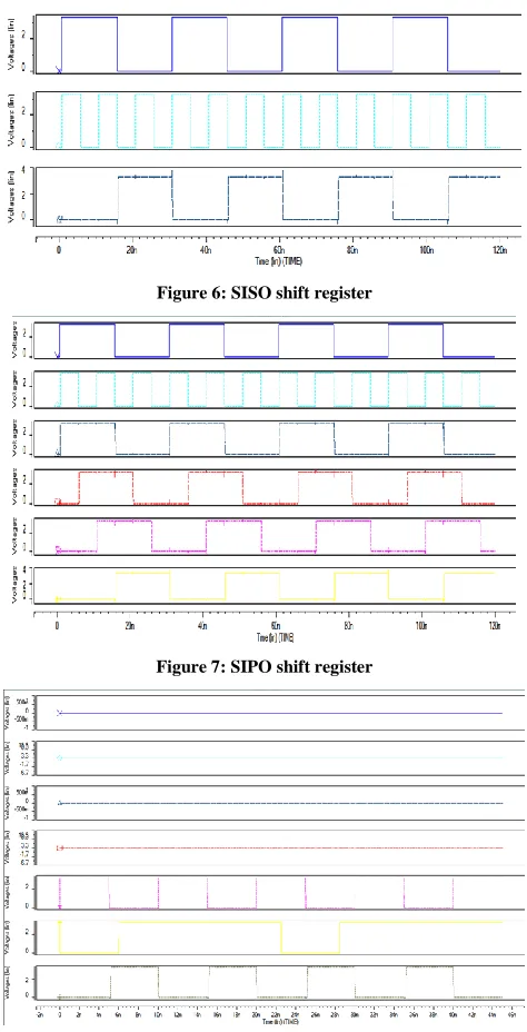
To evaluate the performance, all the shift registers are designed using 130nm CMOS technology. All simulations are carried out using HSPICE simulation tool at nominal conditions with different range of frequencies from 100MHz to 1GHz. The simulated waveforms of the shift registers are shown in Fig. 6, 7, 8 & 9.
These waveforms show that the DETFF based shift register is storing the data in both rising edge and falling edge of the clock signal.
Figure 6: SISO shift register
Figure 7: SIPO shift register
[image:3.612.60.277.394.565.2]International Journal of Emerging Technology and Advanced Engineering
Website: www.ijetae.com (ISSN 2250-2459,ISO 9001:2008 Certified Journal, Volume 3, Issue 2, February 2013)
[image:4.612.57.280.115.322.2]277
Figure 9: PIPO shift register
V. PERFORMANCE ANALYSIS
[image:4.612.331.555.134.596.2]The performance of the SISO, SIPO, PISO and PIPO shift registers are evaluated by considering the average power, delay and power delay product (PDP) for DETFF shown in figure 1. In general, a PDP-based comparison is appropriate for low power portable systems in which the battery life is the primary index of energy efficiency. The following tables from TABLE 1 to TABLE 3 furnished the performance parameters for different range of frequencies from 100MHZ to 1GHZ.
TABLE 1
100MHz CLOCK FREQUENCY
SHIFT
REG.
AVG POWER
(µW)
DELAY
(ns)
PDP
(J)
SISO 26.37 15.21 401.0e-15
SIPO 26.37 0.16
5.20
10.1
15.21
4.219e-15
137.1e-15
266.3e-15
401.0e-15
PISO 34.10 15.01 512.0e-15
PIPO 14.01 0.181 254.8e-17
TABLE 2
500MHz CLOCK FREQUENCY
SHIFT
REG.
AVG POWER
(µW)
DELAY
(ns)
PDP
(J)
SISO 153.0 3.21 491.1e-15
SIPO 153.0 0.20
1.20
2.21
3.21
30.6e-15
183.6e-15
338.1e-15
491.1e-15
PISO 179.2 3.01 540.7e-15
PIPO 67.80 0.182 123.6e-16
TABLE 3 1GHz CLOCK FREQUENCY
SHIFT
REG.
AVG POWER
(µW)
DELAY
(ns)
PDP
(J)
SISO 274.8 1.71 469.9e-15
SIPO 274.8 0.16
0.70
1.05
1.71
43.96e-15
192.3e-15
288.5e-15
469.9e-15
PISO 324.5 1.51 491.9e-15
PIPO 176.5 0.184 325.1e-16
VI. CONCLUSION
[image:4.612.52.285.473.692.2]International Journal of Emerging Technology and Advanced Engineering
Website: www.ijetae.com (ISSN 2250-2459,ISO 9001:2008 Certified Journal, Volume 3, Issue 2, February 2013)
278
REFERENCES
[1] Ravi.T, Irudaya Praveen.D and Kannan.V, ―Design and Analysis of High Performance Double Edge Triggered D-Flip Flop,‖ International Journal of Recent Technology and Engineering (IJRTE), Volume-1, Issue-6, pp. 139-142 January 2013.
[2] Imran Ahmed Khan, Danish Shaikh and Mirza Tariq Beg,, ―2 GHz Low Power Double Edge Triggered flip- flop in 65nm CMOS Technology,‖ IEEE Conference, 2012.
[3] Xiaowen Wang and William H. Robinson, ―A Low-Power Double Edge-Triggered Flip-Flop with Transmission Gates and Clock Gating,‖ IEEE Conference, pp 205-208, 2010.
[4] Yu Chien-Cheng,, ―Low-Power Double Edge- Triggered Flip-Flop Circuit Design,‖ Third International Conference on Innovative Computing Information and Control (ICICIC’08), IEEE Conference, 2008.
[5] G. M. Blair, "Low-power double-edge triggered flip-flop", Electron. Lett., Vol. 33, No. 10, pp. 845-847, 8 May 1997.
[6] Peiyi Zhao, Jason McNeely, Pradeep and Jianping Hu, ‖Low Power Design of Double-Edge Triggered Flip-Flop by Reducing the Number of Clocked Transistors,‖ IEEE Conference, 2008.
[7] Sandeep Sriram, Arun Ramnath, Haiqing, Hojoon Lee and Ken Choi ―A Novel Dual Edge Triggered Near-Threshold State Retentive Latch Design,‖ IEEE Conference, 2011.
[8] M. W. Phyu, W. L. Goh and K. S. Yeo, ―A Low-Power Static Dual Edge-Triggered Flip-Flop using an Output-Controlled Discharge Configuration‖ IEEE Conference, 2005.
[9] M. Pedram, Q. Wu, and X. Wu, ―A New Design of Double Edge Triggered Flip-Flops,‖ Proceedings of the Asia and South Pacific Design Automation Conference (ASP-DAC), pp. 417–421, 1998. [10] Troy A. JohnsonP and Ivan S. Kourtev , ―A Single Latch, High
Speed Double-Edge-triggered flip-flop (DETFF)‖ IEEE, 2001, in press.
[11] Yu Chien-Cheng, ―Design of Low-Power Double Edge-Triggered Flip-Flop Circuit", Second IEEE Conference on Industrial Electronics and Applications, pp 2054-2057, 2007.
[12] S.H.Rasouli, A.Amirabadi, A.Seyedi and A.Afazali-kusha, ―Double Edge Triggered Feedback Flip-Flop in Sub 100nm Technology,‖ IEEE Conference, 2006.
[13] Wing-Shan Tam, Sik-Lam Siu, Chi-Wah Kok, and Hei Wong. ―Double Edge-Triggered Half-Static Clock-Gated D-Type Flip-Flop‖. IEEE International Conference of Electron Devices and Solid-State Circuits (EDSSC), 2010.
[14] Keisuke Inoue and Mineo Kaneko,‖ Variable-Duty -Cycle Scheduling in Double-Edge-Triggered Flip-Flop-Based High-Level Synthesis,‖ IEEE Conference, 2011.
[15] Fatemeh Aezinia, Sara Najafzadeh, and Ali Afzali-Kusha, ―Novel High Speed and Low Power Single and Double Edge-Triggered Flip-Flops,‖ IEEE Conference 2006.
[16] Hossein Karimiyan Alidash, Sayed Masoud Sayedi and Hossein Saidi, ―Low-Power State-Retention Dual Edge-Triggered Pulsed Latch,‖ Proceedings of ICEE 2010, May 11-13, IEEE 2010. [17] M. Pedram, ―Power minimization in IC Design: Principles and
applications,‖ ACM Transactions on Design Automation of Electronic Systems, vol. 1, pp.3-56, Jan. 1996.
[18] G. E. Tellez, A. Farrahi, and M. Sarafzadeh, ―Activity-Driven Clock Design for Low Power Circuits,‖ Proceedings of the IEEWACM International Conference on Computer-Aided Design (ICCAD), pp. 62-65, 1995.
[19] Yingbo Hu, Zhaolin Li and Runde Zhou, ―A New Type of High Performance Low Power Low clock swing TSPC flip-flop,‖ IEEE Conference, 2007.
[20] Guoqiang Hang 1,2, Xuanchang Zhou, ―Novel CMOS Ternary Flip Flops using Double Pass Transistor logic,‖ IEEE Conference, 2011.
First Author: D.Irudaya Praveen was born inPudukkottai, Tamilnadu, India in 1990. He received his Bachelor Degree in Electronics and Communication Engineering from Anna University of Technology, Coimbatore in the year 2011. Currently he is doing his Master Degree in VLSI Design in Sathyabama University, Chennai. His interested areas are Low Power VLSI Design, Advanced digital system design and VLSI Technology.
Second Author: T.Ravi was born in Namakkal, Tamilnadu, India in 1978. He received Master Degree in Applied Electronics from Sathyabama Deemed University in the year 2004. Currently he is doing PhD in Sathyabama University. He is working as Assistant Professor in Department of VLSI Design in Sathyabama University. His interested areas of research are Nano Electronics, VLSI Design, Low Power VLSI Design and Mixed Signal circuits. He has Research publications in National / International Journals /Conferences. He is a member of VLSI Society of India.
![Figure 1: High performance detff [1]](https://thumb-us.123doks.com/thumbv2/123dok_us/8732598.887438/2.612.57.279.606.709/figure-high-performance-detff.webp)