International Journal of Emerging Technology and Advanced Engineering
Website: www.ijetae.com (ISSN 2250-2459,ISO 9001:2008 Certified Journal, Volume 5, Issue 4, April 2015)
482
“To Improve the Output Current of Dynamic Cmos Logic
Circuit with Stack Tachniques”
Neeraj Kumar
1, Ashish Raghuwanshi
21,2
IES College Bhopal
Abstract-- There are several techniques that reduce the rise time and fall time. In this dissertation we can use stack techniques that can improve output current or fan-out. When we are reducing dynamic CMOS noise then it improves the switching speed and output current of dynamic logic circuit. That means improvement of output current is also dependent on the reduction of dynamic logic CMOS noise. Since noise is basically result of charge leakage and charge sharing problem. That means if we can reduced the charge leakage and charge sharing problem then it can reduced the noise of dynamic logic CMOS circuit and it also improves the output current of dynamic logic CMOS circuit. Stack transistors has proven to be exceedingly most effective in reducing and minimizing sub threshold leakage or charge leakage in stand by mode of operation of circuit. It has been observed that this technique of using stack transistors saves around 33% in total leakage in 50nm devices.
Keywords-- Micro wind 3.0.
I. INTRODUCTION
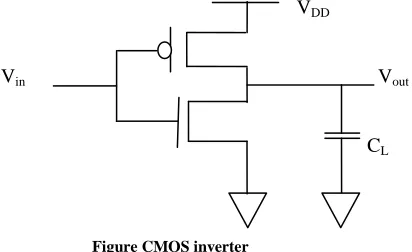
The switching speed of a CMOS gate is dependent on the time taken to charge and discharge the load capacitance. When we are give input transition either 0 or1 then results in an output transition it give either charges (CL) toward VDD or discharges( CL) toward VSS. Now, we
need to define some terms such as Rise, Fall and Delay time
VDD
Vin Vout
CL
[image:1.612.83.289.533.659.2]
Figure CMOS inverter
For the calculation of rise, fall and delay time of the any CMOC logic circuit we are using computer simulation as well as analytical techniques.
Whenever we are using more complex CMOS logic circuit then we are considering appropriate transistor model for the simulation of Dynamic CMOS logic circuits.
• Switching speed: Time taken by wave form to reach
charge and discharge of load capacitance (CL).
• Rise time tr : Time taken by wave form to reach from
10% to 90% of its steady state value.
• Fall time tf : Time taken bywave form to reach from
90% to 10% of steady state value.
• Delay time td : time difference between input
transition (50%) and 50% output level.
II. PROBLEM’S ANALYZED
In this paper there are certain issues of process variations, timing, noise tolerance, and power which are looked into together for operation optimization [2]. We recommend stack technique to improve following aspects:-
To improve charge sharing, charge leakage
problem in dynamic CMOS circuits.
Optimize dynamic CMOS circuits with stack
technique to enable and improve the rise time, fall time, when we equate them to their initial performances.
III. PREVIOUS WORK
In this section we discussed the previous approaches which are nearly related to our research. Here we analyse previous technique that primarily target for reducing rise time and fall time. These techniques are shown in below. The approaches that are adopted in VLSI design. Hear we are using base case, raising source voltage using keepers, source voltage using NMOS, source voltage using PMOS, Feedback Keeper and Pre-charge internal nodes.
Source voltage using PMOS :-
International Journal of Emerging Technology and Advanced Engineering
Website: www.ijetae.com (ISSN 2250-2459,ISO 9001:2008 Certified Journal, Volume 5, Issue 4, April 2015)
483
[image:2.612.327.558.113.297.2]Besides, due to the body effect, transistor threshold voltage is increased when the source voltage rises up. This also aid’s to improve gate turn-on voltage.
Fig. of source voltage using PMOS
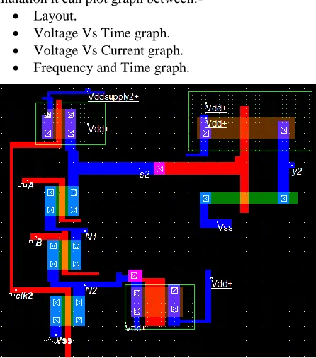
Layout of source voltage using PMOS:-
Firstly, we can draw inverter in DSCH screen. For this we can used 2-PMOS, 3-NMOS, Supply, Ground, 1-Butten, 1-LED, 1-NOT gate and connecting wire that can used to give proper connection. Through this we can design source voltage using PMOS. After the completion of design it save in .MSK format.
Now, we are open Micro wind screen and open saved file. It can generate Lay-out of design circuit, after simulation it can plot graph between:-
Layout.
Voltage Vs Time graph.
Voltage Vs Current graph.
Frequency and Time graph.
[image:2.612.76.260.170.319.2]Fig. Layout of source voltage using PMOS
Fig Simulation of source voltage using PMOS
Parametric analysis of source voltage using PMOS:-
Through this table we can give the value of output current for source voltage using PMOS. This table also shows that the source voltage using PMOS improves the output current.
Parametric analysis table:
Parametric analysis table of source voltage using PMOS
Parameter Output current(mA)
Value 0.424
Source voltage using NMOS:
[image:2.612.57.280.440.693.2]International Journal of Emerging Technology and Advanced Engineering
Website: www.ijetae.com (ISSN 2250-2459,ISO 9001:2008 Certified Journal, Volume 5, Issue 4, April 2015)
484
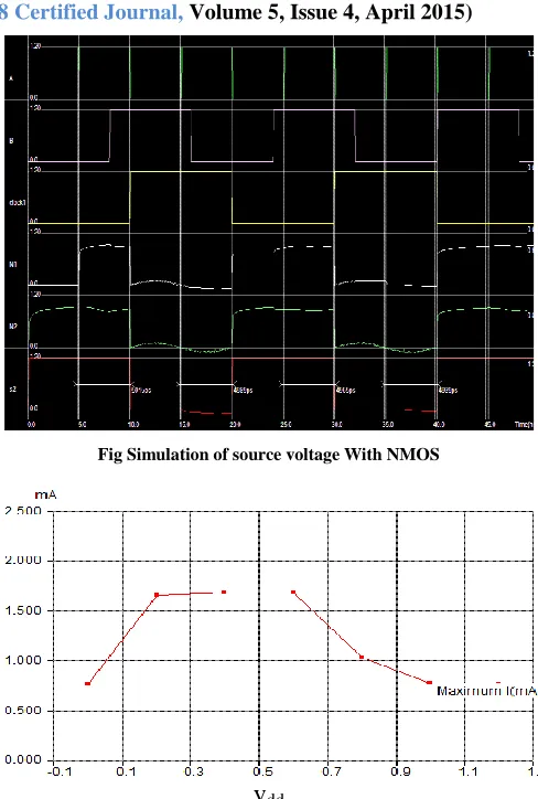
Fig. of source voltage using NMOSLayout of source voltage using NMOS:- Firstly, we can draw source voltage using NMOS in DSCH screen. For this we can used PMOS, 4-NMOS, Supply, Ground, 1-Butten, 1-LED, 1-NOT gate and connecting wire that can used to give proper connection . Through this we can design source voltage using NMOS. After the completion of design it save in .MSK format.
Now, we are open Micro wind screen and open saved file. It can generate Lay-out of design circuit, after simulation it can plot graph between:-
Layout.
Voltage Vs Time graph.
Voltage Vs Current graph.
[image:3.612.322.566.115.477.2] Frequency and Time graph.
Fig Layout of source voltage with NMOS
Fig Simulation of source voltage With NMOS
v
ddFig V/I graph of source voltage with NMOS
Parametric analysis table of source voltage using NMOS:-
Through this table we can give the value of output current for source voltage using NMOS. This table also shows that the source voltage using NMOS improves the output current.
Parametric analysis table:
Parametric analysis table of source voltage using NMOS
Parameter Output current (mA)
Value
0.497
Feedback Keeper:
[image:3.612.74.272.118.301.2] [image:3.612.50.295.431.685.2]International Journal of Emerging Technology and Advanced Engineering
Website: www.ijetae.com (ISSN 2250-2459,ISO 9001:2008 Certified Journal, Volume 5, Issue 4, April 2015)
485
[image:4.612.62.273.159.311.2]Performance degradation and increase in area are the limitations along with the limitation of sleep technique.
Fig. Feedback keeper
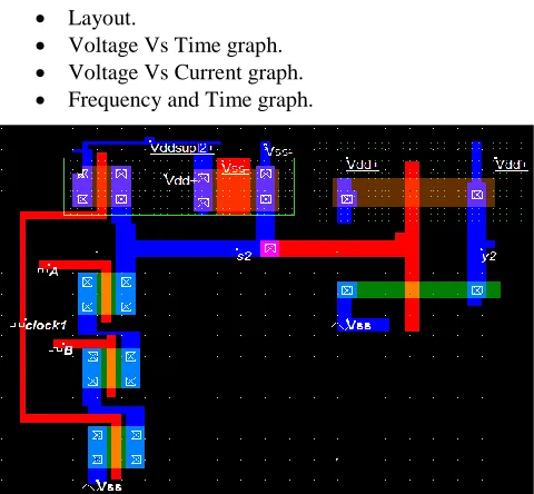
Layout design of feedback keeper logic:-
Firstly, we can design of feedback keeper logic in DSCH screen. For this we can used 1-PMOS, 2-NMOS, 1-Supply, 1-Ground, 1-Butten, 1-LED, 1-NOT gate,1-PDN and connecting wire that can used to give proper connection . Through this we can design of feedback keeper logic. After the completion of design it save in .MSK format.Now, we are open Micro wind screen and open saved file. It can generate Lay-out of design circuit, after simulation it can plot graph between:-
Layout.
Voltage Vs Time graph.
Voltage Vs Current graph.
Frequency and Time graph.
Fig. Layout design of feedback keeper logic
Fig. Simulation of Layout design of feedback keeper logic
v
ddFig V/I graph of feedback keeper
Parametric analysis table of feedback keeper:-
Through this table we can give the value of output current for feedback keeper. This table also shows that the feedback keeper improves the output current.
Parametric analysis table:
Parametric analysis table of feed back keeper
Parameter Output current (mA)
Value 0.0025
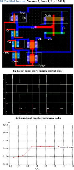
Pre-charge internal nodes:
A simple yet effective way to prevent the charge sharing problem is to pre-charge the internal nodes in the
[image:4.612.324.558.162.486.2] [image:4.612.50.290.437.659.2]International Journal of Emerging Technology and Advanced Engineering
Website: www.ijetae.com (ISSN 2250-2459,ISO 9001:2008 Certified Journal, Volume 5, Issue 4, April 2015)
486
An example dynamic 2-input AND gate using this technique is illustrated in Fig.4.5.1When all internal nodes are pre-charged, this technique is able to eliminate the charge sharing problem at the cost of using a large number of pre-charge transistors and the increased load capacitance on the clock net. Finally, it is noted that techniques based on pre-charging internal nodes alone are not very effective
[image:5.612.316.567.116.690.2]against external noises.
Fig. Pre-charging internal nodes
Layout design of Pre-charging internal nodes logic:-
Firstly, we can design Pre-charging internal nodes logic in DSCH screen. For this we can used 3-PMOS, 3-NMOS, 1-Supply, 1-Ground, 1-Butten, 1-LED, 1-NOT gate,1-PDN and connecting wire that can used to give proper connection . Through this we can design of Pre-charging internal nodes logic. After the completion of design it save in .MSK format.
Now, we are open Micro wind screen and open saved file. It can generate Lay-out of design circuit, after simulation it can plot graph between:-
Layout.
Voltage Vs Time graph.
Voltage Vs Current graph.
Frequency and Time graph.
[image:5.612.325.565.126.370.2]Fig Layout design of pre-charging internal nodes
Fig Simulation of pre-charging internal nodes
V
dd [image:5.612.51.285.230.429.2]International Journal of Emerging Technology and Advanced Engineering
Website: www.ijetae.com (ISSN 2250-2459,ISO 9001:2008 Certified Journal, Volume 5, Issue 4, April 2015)
487
Parametric analysis table of pre-charging internal nodes:-Through this table we can give the value of rise time, fall time and output current for pre-charging internal nodes. This table also shows that the pre-charging internal nodes to improves the output current.
Parametric analysis table:
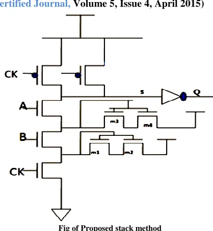
IV. PROPOSED METHODOLOGY
In stack technique, 1-MOS transistor is divided into two half size transistors. When these MOS transistors are turned off together, it induces reverse bias between them which results in the reduction of sub threshold leakage power. However, with increase in the number of transistors overall propagation delay of the circuit increases [12]. Using CMOS technology is basically for consuming less power. In this design criterion it focuses on sub threshold leakage power consumption and it also focuses on body biasing effect and stack effect. One of the main contributors for the static power consumption is sub threshold leakage current which is shown in the Figure i.e. the drain to source current when the gate voltage is smaller than the threshold voltage (Vt). As the technology feature size shrink sub current is
increases exponentially as the decrease of threshold voltage. Stacking transistor can reduce sub-threshold leakage. So it is called stacked effect. Where two or more stack transistors are turning off together, then result can reduce.
[image:6.612.336.545.117.344.2]In complex dynamic logic gates with large pull-down network, charge sharing between the dynamic node and the internal nodes in the pull-down network often results in forged gate switching. A simple yet efficient way to avoid the charge leakage problem is to use stack of transistors in the pull-down network. An example dynamic 2-input AND gate using this technique is illustrated in Fig. In this width of stack of transistors is less than
Fig of Proposed stack method
In this width of stack of transistors is less than width of other transistors , Like if we take width of other transistors as W, than the width of stacked transistors to be taken as w/2. After implementing this design on software we found
that found output current is more and delays found isless
Layout of propose stack method :-
Firstly, we can draw propose stack circuit in DSCH screen. For this we can used 2-PMOS, 7-NMOS, 1-Supply, 1-Ground, 1-Butten, 1-LED, and connecting wire that can used to give proper connection . Through this we can design propose stack circuit. After the completion of design it save in .MSK format.
Now, we are open Micro wind screen and open saved file. It can generate Lay-out of design circuit, after simulation it can plot graph between :-
Layout.
Voltage Vs Time graph.
Voltage Vs Current graph.
Frequency and Time graph.
Parametric analysis table of per charging internal node
Parameter Output current (mA)
International Journal of Emerging Technology and Advanced Engineering
Website: www.ijetae.com (ISSN 2250-2459,ISO 9001:2008 Certified Journal, Volume 5, Issue 4, April 2015)
[image:7.612.50.288.122.510.2]488
Fig Layout of propose stack methodFig Simulation of Propose stack method
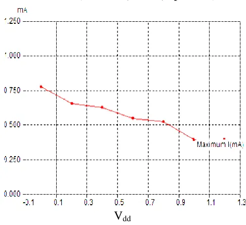
V
ddFig V/I graph of propose stack method
Parametric analysis table of propose stack:-
For the solution of this problem we can used a technique that is called Stack technique. Through this we can improve the Switching speed or response of design circuitry. This technique is also used to reduce leakage current that can improve static power also. Through this table we can give the value of rise time, fall time and output current. This table also shows that the stack technique improves the output current.
Parametric analysis table
Parametric analysis table of propose stack method
Parameter Output current (mA)
[image:7.612.323.566.125.347.2]International Journal of Emerging Technology and Advanced Engineering
Website: www.ijetae.com (ISSN 2250-2459,ISO 9001:2008 Certified Journal, Volume 5, Issue 4, April 2015)
489
V. EXPERIM RESULT
After implementing certain methods, we have found that stack method has proven to be decreasing rise time and fall time, further it has found that delay is also reduced compared to other techniques.
Comparative result analysis:
As we have compared different techniques of decreasing elements malfunctioning circuits like noise, charge leakage, charge sharing & delay. The comparison is shown in table. The comparison has clearly proved that proposed logic has proven advanced than other ones.
Comparative Parametric analysis table:
In this table we are giving output current values for all previous approaches and proposed stack technique. Through this table we compare output current and says whose technique is best all of them.
Cell Output current (mA) Source volt with NMOS 0.497
Source volt with PMOS 0.424
Feedback Keeper 0.0025
Pre-charging internal node 0.47
Proposed stack logic 0.559
VI. CONCLUSION
Noise or any unwanted signal when enters in a system malfunctions the system, there are various types of noise mainly Thermal noise, Flicker noise ,Voltage transition , etc. All these noises adversely affects the system, there could be certain measures , with the help of which we can decrease noise to a certain extent. Major factor which causes noise are charge leakage and charge sharing problems , thus by using stack transistors we can minimize charge leakage and charge sharing problem and hence minimize noise. The most commonly used dielectric is silicon–di-oxide ,But if we uses high K dielectric material we can minimize noise because the conventional silicon-di-oxide film is too thin e.g. 2nm, to minimize the tunneling current. Thus a slight modification could be done that is The Equivalent Oxide Thickness (EOT) is an essential terminology in high-k field, which indicates how thick a silicon oxide layer would need to be in order to produce the same effect as the high-k material being used. Because the conventional SiO2 film is so thin (e.g. 2 nm) to minimize the tunnelling current and the out diffusion of boron from the gate.
If we deposit high-k dielectric materials directly on silicon it results in a very poor interface, and which even has a large amount of defects. A critical solution of this
form of a thin SiO2 layer 0.5-0.7nm before deposition of
high-k oxide layer with this a high-quality interface between high-k oxides and silicon is restored. The degree to which Noise occurs within a circuit can to a great degree determine the reliability of a circuit. Designers should be versed in knowing about Noise, predicting the occurrences of Noise, and limiting the frequency of Noisy outputs. Ways of limiting Noise include using only one clock, using faster flip-flops, and decrease the asynchronous input frequency, and use synchronization hardware. These steps may easy be get by designers to increase the reliability of a circuit.
Charge sharing & charge leakage problem is
minimized.
Output current has been enhanced.
Delay has been reduced that means improve switching
response.
VII. FUTURE SCOPE
In this method we can improve the output current. In future we are having a target to improve rise time, fall time and power dissipation so in future we can develop a new method that can overcome this problem
REFERENCES
[1] Hailong Jiao, Student Member, and Volkan Kursun publish their paper on title "Reactivation Noise Suppression With Sleep Signal Slew Rate Modulation in MTCMOS Circuits" in IEEE transactions on very large scale integration (vlsi) systems, vol. 21, no. 3, march 2013.
[2] Kumar Yelamarthi, and Chien-In Henry Chen "Timing Optimization and Noise Tolerance for Dynamic CMOS Susceptible to Process Variations" IEEE transactions on semiconductor manufacturing, vol. 25, no. 2, may 2012.
[3] Massimo Alioto,Gaetano Palumbo, and Melita Pennisi "Understanding the Effect of Process Variations on the Delay of Static and Domino Logic" IEEE transactions on very large scale integration (vlsi) systems, vol. 18, no. 5, may 2010.
[4] Gaetano Palumbo, Melita Pennisi, Member. and Massimo Alioto "A Simple Circuit Approach to Reduce Delay Variations in Domino Logic Gates" IEEE transactions on circuits and systems iregular papers, vol.59, no.10, october 2012.
[5] You-Gang Chen, I-Chyn Wey, and An-Yeu (Andy) Wu “A New Noise-Tolerant Dynamic Circuit Design with Enhanced PDP Performance under Low SNR Environment” Graduate Institute of Electronics Engineering, National Taiwan University, Taiwan [6] Farzan Fallah Fujitsu Labs. of America, Inc. Advanced CAD
International Journal of Emerging Technology and Advanced Engineering
Website: www.ijetae.com (ISSN 2250-2459,ISO 9001:2008 Certified Journal, Volume 5, Issue 4, April 2015)
490
[7] Massimo Alioto,Gaetano Palumbo,and Melita Pennisi "Understanding the Effect of Process Variations on the Delay of Static and Domino Logic" IEEE transactions on very large scale integration (vlsi) systems, vol. 18, no. 5, may 2010. Implementation of charge leakage and sharing noise susceptible dynamic CMOS design.
[8] P. Magnone, F. Crupi, G. Giusi, C. Pace, E. Simoen, C. Claeys, Fellow, IEEE, L. Pantisano, D. Maji, V. Ramgopal Rao, Senior Member, IEEE, and P. Srinivasan “1/f Noise in Drain and Gate Current of MOSFETs With High-k Gate Stacks”.
[9] You-Gang Chen, I-Chyn Wey, and An-Yeu (Andy) Wu Graduate Institute of Electronics Engineering, National Taiwan University, Taiwan “A New Noise- Tolerant Dynamic Circuit Design with Enhanced PDP Performance under Low SNR Environment”
[10] E-238 Analog VLSI Circuits Dr. Navakanta Bhat ECE department Indian Institute of science Banglore 560012 August 2005.
[11] Razak Hossain “High Performance ASIC Design Using Synthesizable Domino Logic in an ASIC Flow” Cambridge University Press.