International Journal of Emerging Technology and Advanced Engineering
Website: www.ijetae.com (ISSN 2250-2459,ISO 9001:2008 Certified Journal, Volume 4, Issue 9, September 2014)
677
Implementation of UART with BIST Technique in
System-on-Chip (SOC)
G. Srilatha
1, D. Kavitha
2, G. Sanath Kumar
31M.Tech –VLSI (pursuing) in ASTRA, JNTUH University, Telangana, India. 2Internal Guide, Associate professor in ASTRA, JNTUH University, Telangana, India. 3External Guide, Dy Director of Training Department in CITD, Balanagar, Hyderabad, India. Abstract-- In today’s life the most Manufacturing processes
are extremely complex, including manufacturers to consider testability as a requirement to assure the reliability and the functionality of each of their designed circuits. One of the most popular test techniques is called Built-In-Self-Test (BIST). A Universal Asynchronous Receiver and Transmitter (UART) with BIST capability has the objectives of testing the UART on chip itself and no external devices are required to perform the test. This paper focuses on the VERILOG implementation of UART with BIST capability using SOC technology. This paper presents the architecture of UART with BIST which tests the UART for its correct ability. The whole design is simulated in cadence IUS and synthesized using RTL compiler and implemented on SOC encounter.
Keywords-- UART, BIST, SOC DFT, BRG, ATE.
I. INTRODUCTION
Universal Asynchronous Receiver and Transmitter (UART) is a kind of serial communication protocol; mostly used for short-distance, low speed, low-cost, data exchange between computer and peripherals. UARTs are used for asynchronous serial data communication by converting data from parallel to serial at transmitter with some extra overhead bits using shift register and vice versa at receiver. It is generally connected between a processor and a peripheral, to the processor the UART appears as an 8-bit read/write parallel port.
Built-In-Self-Test or BIST, is the technique of designing additional hardware and software features into integrated circuits to allow them to perform self-testing, i.e., testing of their own operation using their own circuits, thereby reducing dependence on external Automated Test Equipment (ATE)[6]. BIST is a Design-For-Testability (DFT) technique, because it makes the electrical testing of a chip easier, faster, more efficient, and less costly. The concept of BIST is applicable to just about any kind of circuit, so its implementation can vary as widely as the product diversity that it caters to.
Advantages of implementing BIST include: lower cost of test, since the need for external electrical testing using an ATE will be reduced, if not eliminated; better fault coverage, since special test structures can be incorporated onto the chip; shorter test times if the BIST can be designed to test more structures in parallel; easier customer support; and capability to perform tests outside the production electrical testing environment [6].
The rest of paper is as follows. The advantages of Verilog are highlighted in section II. Section-III describes the UART architecture along with algorithms. Section-IV describes the architecture of UART with BIST capability. Section-V describes the LFSR design. Section-VI illustrates the simulation results of each module using cadence IUS. In Section-VII finally the paper is concluded.
II. VERILOG IMPLEMENTATION
The detail design of systems at the gate and flip-flop level has become time consuming as the integrated circuit technology has become very complex [1]. In recent years this fact has motivated usage of hardware description language (HDL) in the design process of digital system. Verilog is used to describe and simulate the operation of variety of digital system which is ranging in complexity from a few gates to an interconnection of many complex integrated circuits. Advantages of verilog implementation includes: minimum cost and time, better design, faster time to market and increased flexibility [1].
III. UARTARCHITECTURE
International Journal of Emerging Technology and Advanced Engineering
Website: www.ijetae.com (ISSN 2250-2459,ISO 9001:2008 Certified Journal, Volume 4, Issue 9, September 2014)
678
Figure1. Frame Format for UART
The design of UART, shown in fig.2, has Baud Rate Generator (BRG), Transmitter and Receiver as its functional units. All these blocks are explained in brief in the rest of this section.
Figure2. UART Architecture
A. Baud Rate Generator
The baud rate generator is used to produce local clock signal which is much higher than the baud rate to the UART receiver and transmitter. The baud rate generator is actually a frequency divider. The frequency factor is calculated according to the given system clock frequency and requested baud rate. Assume that the system clock is 50MHZ, baud rate is 9600bps. Therefore the frequency coefficient (M) of baud rate generator is:
M = 50*10^6/9600Hz=5200
B. Transmitter
The transmitter section accepts parallel data, makes the frame of the data and transmits the data in serial form on the Transmitter output (TXOUT) terminal. Data is loaded from the inputs TXIN0-TXIN7 into the transmitter FIFO by applying logic high on the WR (write) input. If words less than 8 bits are used, only the least significant bits are transmitted.
FIFO is 16-byte register. When FIFO contains some data, it will send the signal to Transmitter Hold Register (THR), which is an 8-bit register. At a same time, if THR is empty it will send the signal to FIFO, which indicates that THR is ready to receive data from FIFO. If the Transmitter Shift Register (TSR), is empty it will send the signal to THR and it indicates that TSR is ready to receive data from THR. TSR is 11-bit register in which framing process occurs. In frame start bit, stop bit, and parity bit will be added. Now data is transmitted from TSR to TXOUT serially. The Transmitter diagram is shown in fig.3.
Figure3. UART Transmitter
C. Receiver
The transmitted data from the TXOUT pin is available on the RXIN pin. The received data is applied to the sampling logic block. The receiver timing control is used for synchronization of clock signal between transmitter and receiver.
International Journal of Emerging Technology and Advanced Engineering
Website: www.ijetae.com (ISSN 2250-2459,ISO 9001:2008 Certified Journal, Volume 4, Issue 9, September 2014)
679
[image:3.612.64.277.176.323.2]If the RXIN pin is held for long time than the frame time then there is a break in received data and break error occurs and BL bit is set. The Receiver diagram is shown in fig.4.
Figure 4. UART Receiver
IV. ARCHITECTURE OF UARTWITH BIST
The architecture proposes an 8-bit UART which operates at a baud rate of 9600bps with a status register to monitor the correctness of every received data byte and enhance the testability of circuit by the introduction of BIST module. The hardware architecture of the 8-bit UART with status register, incorporated with BIST module is explained in the following sections.
The architecture model has two major modules they are UART and BIST. Further in the UART, we have transmitter, receiver and baud rate generator. BIST has a control register, pattern generator and a comparator as shown in fig.5.
Figure.5. UART with BIST
For BIST, UART is set in an internal loop back mode (fig.5). This is used to test both the transmitter and receiver of the UART. This will loop back the serial data and transmit the data back to the receiver.
[image:3.612.332.556.365.496.2]For the BIST, the test pattern is generated by LFSR as mentioned in the next section and the pattern is loaded to the FIFO of the UART Transmitter. Each test byte is then padded with start, parity and stop bits and sent from transmitter and is looped back to receiver. The receiver will extract the data from frames received and loads to receiver FIFO. During this the status register flags will be set according to the error check. Then the Transmitter FIFO is compared with receiver FIFO to verify the transmitted data and received data are same. If FIFOs are with same data then BIST pass and bit-0 of control register is set to „1‟, else „0‟. 8-bit BIST control register is defined as below. The register helps in identifying the operation in which BIST failure occurred.
Table.1. BIST control register
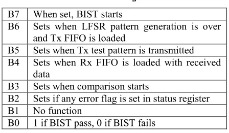
B7 When set, BIST starts
B6 Sets when LFSR pattern generation is over and Tx FIFO is loaded
B5 Sets when Tx test pattern is transmitted B4 Sets when Rx FIFO is loaded with received
data
B3 Sets when comparison starts
B2 Sets if any error flag is set in status register B1 No function
B0 1 if BIST pass, 0 if BIST fails
V. LFSRDESIGN
[image:3.612.59.280.492.639.2]International Journal of Emerging Technology and Advanced Engineering
Website: www.ijetae.com (ISSN 2250-2459,ISO 9001:2008 Certified Journal, Volume 4, Issue 9, September 2014)
[image:4.612.69.257.162.327.2]680
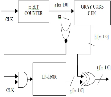
Figure.6 Low power test pattern generator
The m-bit counter is initialized with zeros and which generates 2m test patterns in sequence. A gray code generator and m-bit counter are controlled by common clock signal (CLK). The output of m-bit counter is applied as input to a NOR-gate structure and a gray code generator. When all the bits of counter output are zero, the NOR-gate output is one. Only when the NOR-gate output is one, the clock signal is applied to activate the LP-LFSR which generates the next sequence. The sequence generated from LP-LFSR is exclusive-ORed with sequence generated from gray code generator. The patterns generated from the Exclusive-OR array are the final output patterns.
VI. SIMULATION RESULTS
The Verilog HDL coding and simulation of the design are done in cadence IUS. The operating clock frequency used for simulation is 50MHz. The baud rate set is 9600bps. Data word length is 8-bits.
A. Simulation Results of Transmitter
The fig.7 shows the serial transmission of data and fig.8 shows the Schematic view of UART transmitter. Data transmitted is „11111111‟. The 8-bit data is loaded to transmit shift register and start, stop and parity bits are added to form the frame inside TSR and sent to TXD.
[image:4.612.324.568.205.501.2]When the reset is 0 and transmit is 1, the transmitter starts transmitting the data. i.e. the data start shifting out from the transmitter shift register. The serial transmission is observed at TXD pin along with frame format (1 logical low start bit, 8-bit data (LSB to MSB), parity bit and finally logical high stop bit).
Figure 7: Simulation results of UART transmitter
Figure 8: Schematic view of UART transmitter
B. Simulation Results of Receiver
International Journal of Emerging Technology and Advanced Engineering
Website: www.ijetae.com (ISSN 2250-2459,ISO 9001:2008 Certified Journal, Volume 4, Issue 9, September 2014)
[image:5.612.333.555.108.691.2]681
Figure 9: Simulation Results of UART receiver
Figure 10: Schematic view of UART Receiver
C. Simulation Results of UART module
The UART Transmitter accepts the parallel data and makes the frame of the data and transmits the data in serial form on TXOUT terminal. This serial output is taken as input for the Receiver and receiver sends the parallel data on RxData. Fig.11 shows the simulation of UART, fig.12 shows the Schematic view of UART module and fig.13 shows the internal block of UART which includes baud rate, transmitter and receiver as b0, t0 and r0 respectively.
Figure 11: Simulation Results of UART
Figure 12: Schematic view of UART module
[image:5.612.57.280.122.514.2]International Journal of Emerging Technology and Advanced Engineering
Website: www.ijetae.com (ISSN 2250-2459,ISO 9001:2008 Certified Journal, Volume 4, Issue 9, September 2014)
682
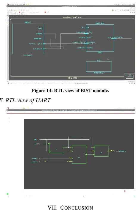
D. RTL view of BIST module
[image:6.612.50.280.207.563.2]The fig. 14 shows the RTL view of BIST module. The pattern generated by LFSR is transmitted from transmitter FIFO and received in receiver FIFO. The transmit FIFO is compared with the receive FIFO; if both the FIFOs are same hence the test status bit is set to „1‟.
Figure 14: RTL view of BIST module.
E. RTL view of UART
VII. CONCLUSION
This paper describes the architecture of UART with BIST technique which will test that the UART is working properly not. Working principle of this BIST technique has been tested by considering UART as a digital circuit test using cadence IUS and which can be implemented on SOC.
REFERENCES
[1] Idris, M.Y.I.; Yaacob, M.;, "A VHDL implementation of BIST
technique in UART design," TENCON 2003. Conference on Convergent Technologies for Asia-Pacific Region , vol.4, no., pp. 1450- 1454 Vol.4, 15-17 Oct. 2003.
[2] Fang Yi-Yuan; Chen Xue-jun; , "Design and Simulation of UART Serial Communication Module Based on VHDL," Intelligent Systems and Applications (ISA), 2011 3rd International Workshop on , vol., no., pp.1-4, 28-29 May 2011
[3] Prof Naresh Patel, Vatsal Patel, Vikas Patel,”VHDL Implementation
of UART with Status Register”, Sarvajanik College of Engg. And Technology.
[4] Prof. Rami Abielmona, “Project: UART Design”, for CEG 3150:
Digital Systems-II, fall 2004, November 24, 2004.
[5] Mohd.Yamani Idna Idris, Mashkuri Yaacob, Zaidi Razak,”A VHDL
Implementation of UART Design With BIST capability”, Faculty of Computer Science and Information Technology, University of Malaya,50603 Kuala Lumpur, Malaysia.\
[6] Shikha kakar, Balwinder Singh, Arun Khosla, ”Implementation of
BIST capability using LFSR technique in UART”, International Journal of Recent Trends in Engineering ,Vol 1, No. 3, May 2009,pp.301-304.
[7] Elmenreich, W.; Delvai, M.;, "Time-triggered communication with
UARTs," Factory Communication Systems, 2002. 4th IEEE International Workshop on, vol., no., pp. 97- 104, 2002J. Clerk Maxwell, A Treatise on Electricity and Magnetism, 3rd ed., vol. 2. Oxford: Clarendon, 1892, pp.68–73.
[8] Gallo, R.; Delvai, M.; Elmenreich, W.; Steininger, A.;, "Revision and verification of an enhanced UART," Factory Communication Systems, 2004. Proceedings. 2004 IEEE International Workshop on, vol., no., pp. 315- 318, 22-24 Sept. 2004.
[9] Norhuzaimin, J.; Maimun, H.H.;, "The design of high speed UART,"
Applied Electromagnetics, 2005. APACE 2005. Asia-Pacific Conference on, vol., no., pp.5 pp., 20-21 Dec. 2005.
[10] Himanshu Patel; Sanjay Trivedi; R. Neelkanthan; V. R. Gujraty; , "A
Robust UART Architecture Based on Recursive Running Sum Filter for Better Noise Performance," VLSI Design, 2007. Held jointly with 6th International Conference on Embedded Systems., 20th International Conference on, vol., no., pp.819-823, Jan. 2007.
[11] Yongcheng Wang; Kefei Song; , "A new approach to realize
International Journal of Emerging Technology and Advanced Engineering
Website: www.ijetae.com (ISSN 2250-2459,ISO 9001:2008 Certified Journal, Volume 4, Issue 9, September 2014)
683
AUTHOR‟S PROFILE
G. SRILATHA received B.Tech degree in ECE from Bhoj Reddy Engineering College for Women in 2012, pursuing M.Tech (2012-2014) in the stream of VLSI at (ASTRA) Aurora‟s Scientific, Technological and Research Academy, (Affiliated to JNTUH) Hyderabad.
Mrs. D. KAVITHA received M.Tech degree in VLSI from JNTUH in 2010, B.E degree in ECE from OU in 2003, Diploma in ECE from SBTET in 1998. Presently working as Associate professor in ASTRA, Hyd.
G. SANATH KUMAR Dy. Director