International Journal of Emerging Technology and Advanced Engineering
Website: www.ijetae.com (ISSN 2250-2459,ISO 9001:2008 Certified Journal, Volume 3, Issue 9, September 2013)
260
Comparative Analysis of Conventional CMOS and Energy
Efficient Adiabatic Logic Circuits
Gaurav Singh
1, Ravi Kumar
2, Manoj Kumar
Sharm31,2
Department of Electronics & Communication Engineering, IMS Engineering College Ghaziabad, UP.
3Department of Electronics & Communication Engineering, Vidya Enggineering college, bhagpat road, Meerut, UP.
Abstract--In recent years, low power circuit design has been an important issue in System on Chip (SoC) and VLSI design areas. Adiabatic logics, which dissipate less power than static CMOS logic, have been introduced as a promising new approach in low power circuit design. Adiabatic circuits are those circuits which work on the principle of adiabatic charging and discharging and which recycle the energy from output nodes instead of discharging it to ground. This paper proposes a Adder circuit based on energy efficient adiabatic logic, a simulative investigation on the proposed 1-bit full adder has been implemented with the proposed technique. In
this paper conventional complementary metal oxide
semiconductor (CMOS) and adiabatic adder circuits are analyzed in terms of power dissipation using 0.35UM technology.
Keywords--Low-power, adiabatic logic, Full adder, CMOS, Positive feed back adiabatic logic, 2PASCAL
I. INTRODUCTION
Very recently, it has been envisaged that demand for ultralow power systems has attracted many researcher’s interest in the development of technically acceptable low power VLSI design methodologies as compared to traditional age old strategies. In conventional CMOS circuits, power dissipation can be minimized by reducing the supply voltage, node capacitance, and switching activity to a certain extent but very nascent adiabatic computing has appeared as anaturally acceptable and very practical solution in low power VLSI systems. Several adiabatic logic families based onenergy recovery principle where all charge recovered back to power supply without heat generation have beenproposed & implemented earlier. The low-power requirements of present electronic systems have challenged the scientific research towards the study of technological, architectural and circuital solutions that allow a reduction of the energy dissipated by an electronic circuit. One of the main causes of energy dissipation in CMOS circuits is due to the charging and discharging of the node capacitances of the circuits, present both as a load and as parasitic. Such part of the total power dissipated by a circuit is called dynamic power.
In order to reduce the dynamic power, an alternative approach to the traditional techniques of power consumption reduction, named adiabatic switching, has been proposed in the last years. In such approach, the process of charging and discharging the node capacitances is carried out in a way so that a small amount of energy is wasted and a recovery of the energy stored on the capacitors is achieved. In literature, various kinds of adiabatic circuits proposed all of them can be grouped into two fundamental classes: fully adiabatic circuits and quasi-adiabatic or partial energy recovery circuits. In the first class, in particular working conditions can consume asymptotically zero energy for operation, the large area occupation and the design complexity make these circuits not competitive with traditional CMOS where as in second class circuits designed to recover large portion of the energy stored in the circuit node capacitances. This energy loss drawback however allows a good trade-off between circuit complexity and then area occupation.In this paper different circuit are presented, and comparison of conventional CMOS adder circuits [1][2][4][5][6], 2PASCAL [10] ,and also comparison of adiabatic families[3][7][8][9] is done. In this work we analyzed the performance of conventional and adiabatic adder circuit’s in-terms of power consumption.
This paper has been segmented into four sections. The section II describes the working adiabatic logic whereas Section III & IV are all about simulation results and conclusion.
II. ADIABATIC SWITCHING
In the following section conventional switching and adiabaticswitching analyzed in detail.
2.1 Conventional Switching
International Journal of Emerging Technology and Advanced Engineering
Website: www.ijetae.com (ISSN 2250-2459,ISO 9001:2008 Certified Journal, Volume 3, Issue 9, September 2013)
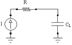
261 The equivalent circuits of CMOS logic for charging and discharging is shown in Fig.1. The expression for total power dissipation is given by-
Ptot = α .CL .V .Vdd. fclk + Isc .Vdd + Ile .Vdd (1)
Equation (1), the first term represents the dynamic power, where CLis the loading capacitance, fclkis the clock frequency, and α is the switching activity. In most cases, the voltage swing V is the same as the supply voltage Vdd however, in some logic circuits, the voltage swing on some internal nodes may be slightly less. The second term is due to the direct-path short circuit current Isc which arises when both the NMOS and PMOS transistors are simultaneously active, conducting current directly from supply to ground. Finally, leakage current Ile which can
[image:2.612.87.240.343.449.2]arise from substrate injection and sub threshold effects is primarily determined by fabrication technology considerations[11][12].
Figure 1 Conventional CMOS a) Charging b) Discharging
2.2 Adiabatic Switching
Adiabatic switching can be achieved by ensuring that the potential across the switching devices is kept arbitrarily small. This can be achieved by charging the capacitor from a time-varying voltage source or constant current source[12][13][14] as shown in Fig. 2. Here, R represents the on resistance of the PMOS network. Also note that a constant charging current corresponds to a linear voltage ramp. Assuming that the capacitance voltage VC is zero initially, the variation ofthe voltage as a function of time can be found as
Figure 2 Schematic for adiabatic charging process
Vc (t ) = Is .t / 2 (2)
Hence the charging current can be expressed as a function of VC and time t
Is = C.Vc(t) / 2 (3)
The amount of energy dissipated in the resistor R from t
= 0 to t = T can be found as
Ediss = R. ∫ T
Is 2 dt = R . Is2.T (4)
Combining (3) and (4), the dissipated energy during this charge-up transition can also be expressed as
Ediss = (RC/T).C. Vc2 (T) (5)
From (5) we can say that the dissipated energy is smaller than for the conventional case if the charging time T >>2RC and can be made small by increasing the charging time. A portion of the energy thus stored in the capacitance can also be reclaimed by reversing the current source direction, allowing the charge to be transferred from the capacitance back into the supply. Adiabatic logic circuits thus require non-standard power supplies with time-varying voltage, also called pulsed power supplies. The additional hardware overhead associated with these specific power supply circuits is one of the design trade-off. Practical supplies can be constructed by using resonant inductor circuits. But the use of inductors should be limited from integrated circuit point because of so many factors like chip integration, accuracy, efficiency etc. An alternative to using pure voltage ramps is to use stepwise supply voltage waveforms, where the output voltage of the power supply is increased and decreased in small increments during charging and discharging. Since the energy dissipation depends on the average voltage drop across the resistor by using smaller voltage steps the dissipation can be reduced considerably. The total dissipation using step wise charging is given by (6)
Etdiss = (1/n). C. Vdd2 / 2 (6)
Where n is number of steps used to charge up capacitance to Vdd.
[image:2.612.106.230.610.689.2]International Journal of Emerging Technology and Advanced Engineering
Website: www.ijetae.com (ISSN 2250-2459,ISO 9001:2008 Certified Journal, Volume 3, Issue 9, September 2013)
262 If any voltage difference between the two terminals of a switch exists when it is turned on, non-adiabatic loss occurs. The non-adiabatic loss, which is independent of the frequency of the power-clock, is proportional to the node capacitance and the square of the voltage difference. Several quasi-adiabatic logic architectures have been reported, such as ECRL, 2N-2N-2P, PFAL [13][14][15][16][17]etc.
III. CMOSINVERTER
Power dissipation in conventional CMOS circuits primarily occurs during the device switching. When the logic level in the system is “1,” there is a sudden flow of current through R.
Q = CL.Vdd is the charge supplied by the positive power
supply rail for charging CL to the level of Vdd. Hence, the
energy drawn from the power supply is Q·Vdd = CLVdd2[18]
. By assuming that the energy drawn from the power supply is equal to that supplied to CL, the energy stored in CL is said to be one-half the supplied energy, i.e., Estored = ( 1/2
)CLVdd2. The remaining energy is dissipated in R. The same
amount of energy is dissipated during discharging in the nMOS pull-down network when the logic level in the system is “0.” Therefore, the total amount of energy dissipated as heat during charging and discharging is
Etotal = Echarge + Edischarge
[image:3.612.348.541.347.500.2]= 0.5 CLVdd2 + 0.5 CLVdd2 = CLVdd2
Figure 3 Schematic of CMOS inverter
IV. PROPOSED POSITIVE FEEDBACK ADIABATIC LOGIC
INVERTER-PFAL
The structure of Positive Feedback Adiabatic Logic PFAL logic [19] [20] is shown in figure 4. Two n-trees realize the logic functions. This logic family also generates both positive and negative outputs.
The two major differences with respect to ECRL are that the latch is made by two PMOSFETs and two NMOSFETs, rather than by only two PMOSFETs as in ECRL, and that the functional blocks are in parallel with the transmission PMOSFETs. Thus the equivalent resistance is smaller when the capacitance needs to be charged. The ratio between the energy needed in a cycle and the dissipated one can be seen in figure 4. During the recovery phase, the loaded capacitance gives back energy to the power supply and the supplied energy decreases. The partial energy recovery circuit structure so called Positive Feedback Adiabatic Logic (PFAL) [21], has good robustness against technological parameter variations [22][23]. It is a dual rail circuit; the core of all the PFAL circuit is adiabatic amplifier, a latch made up by the two PMOS and two NMOS that avoids a logic level degradation on the output nodes. The two n-tree release the logic functions. The functional blocks are in parallel with P-MOSFETs and form a transmission gate.
Figure 4 PFAL Logic Circuit
V. 2PASCL
[image:3.612.55.275.422.610.2]International Journal of Emerging Technology and Advanced Engineering
Website: www.ijetae.com (ISSN 2250-2459,ISO 9001:2008 Certified Journal, Volume 3, Issue 9, September 2013)
263 1) Evaluation phase:
a)When the output node Y is LOW and the PMOS tree is turned ON, CL is charged through the PMOS
transistor, and hence, the output is in the HIGH state. b)When node Y is LOW and NMOS is ON, no
transition occurs. c) When the output node is HIGH and the PMOS is ON, no transition occurs. d) When node Y is HIGH and the NMOS is ON, discharging via NMOS and D2 causes the logic state of the output to be “0” [24].
2) Hold phase
a)When node Y is LOW and the NMOS is ON, no transition occurs.
[image:4.612.337.544.112.283.2]b)At the point when the preliminary state of the output node is HIGH and the PMOS is ON, discharging via D1 occurs.
Figure 5 2PASCAL
VI. ADDER IMPLEMENTATION
A basic cell in digital computing systems is the 1-bit full adder which has three bit inputs (A, B, and C) and two 1-bit outputs (sum and carry). The relations between the inputs and the outputs are expressed as
Sum = ABC + ABC + ABC + ABC (8a)
Carry = AB + BC + CA (8b)
6.1 Conventional adder
Conventional CMOS Implementation consists of two functional blocks pull-up and pull-down. Pull-up functional block is implemented with P-channel MOS transistors and pull-downfunctional block is implemented with N-channel MOS transistors. In order to get symmetrical structure (8a) is rearranged as (9) and sum and carry implementation is shown in Fig.7b.
Sum = ABC + (A + B + C)Carry (9)
Figure 6 Conventional Symmetrical CMOS Full Adder
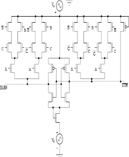
6.2 Proposed PFAL Adder circuit
A partially adiabatic logic family PFAL one-bit Full Adder block can be implemented as shown in the Figure 7( for SUM block) and Figure 8(for CARRY block) below, respectively.
Figure (7a) PFAL one-bit Full Adder( for SUM block)
[image:4.612.60.278.317.490.2] [image:4.612.381.510.373.529.2] [image:4.612.370.520.553.703.2]International Journal of Emerging Technology and Advanced Engineering
Website: www.ijetae.com (ISSN 2250-2459,ISO 9001:2008 Certified Journal, Volume 3, Issue 9, September 2013)
264 VII. SIMULATION RESULTS
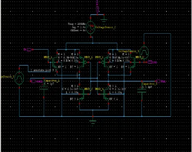
In order to estimate the power dissipation of the different circuits (CMOS inverter, PFAL , 2PASCAL, conventional full adder, proposed 1-bit full adder) presented in previous section we used power meter simulation model presented and RC model presented. The schematic diagram of the test setup to estimate the power dissipation is shown in fig below. All the circuits are designed and simulated using Tanner tools(S-edit, TSPICE) with 0.35um technology parameters. Figure 8 & 9 shows the simulation results of comparison of Conventional CMOS and energy efficient full adder adiabatic logic. Table. I gives power dissipation values under the operating conditions VDD=1.8V, CL=0.1pF
[image:5.612.68.267.385.625.2]and frequency 10MHz.Fig.12 shows the variation of power dissipation with the frequency for the different circuit implementations.
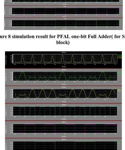
Figure 8 simulation result for PFAL one-bit Full Adder( for SUM block)
Figure 9 simulation result for PFAL one-bit Full Adder( for CARRY block)
VIII. POWER DISSIPATION RESULTS FOR VARIOUS
CIRCUIT
Table 1
IX. CONCLUSION
In this paper we analysed the power dissipation of various circuit shown in Table 1 and comparison of performance of different adiabatic logic adder circuits with traditional CMOS adder circuits. The analysis shows that designs based on adiabatic principle gives superior performance when compared to traditional approaches in terms of power even though their transistor count is high in some circuits so for low power and ultra low power requirements adiabatic logic is an effective alternative for traditional CMOS logic circuit design.
REFERENCES
[1] N. Zhuang and H.Wu, (1992) “A New Design of the CMOS Full Adder,” IEEE Journal of Solid-stateCircuits, Vol. 27, No. 5, pp 840-844.
International Journal of Emerging Technology and Advanced Engineering
Website: www.ijetae.com (ISSN 2250-2459,ISO 9001:2008 Certified Journal, Volume 3, Issue 9, September 2013)
265
[3] R.K. Yadav, A.K. Rana, Shweta Chauhan , Deepesh Ranka and Kamalesh Yadav (2011) “Adiabatic Technique for Energy Efficient Logic Circuits Design” Proceedings of ICETECT pp 776-780 [4] E .S .Chew, M.W. Phyu, and W.L. Goh (2009) “Ultra Low-Power
Full-Adder for Biomedical Applications” IEEE pp115-118. [5] C. H. Chang, J. Gu and M. Zhang, (2005) "A review of 0.18um full
adder performances for tree structured arithmetic circuits," IEEE Transactions on VLSI Systems, vol. 13, no. 6, pp. 686-695. [6] S. Goel, A. Kumar and M. A. Bayoumi,(2006) "Design of robust,
energy efficient full adders for deep-submicrometer design using hybrid CMOS logic style," IEEE Transactions on VLSI Systems, vol.I4, no.12, pp. 1309-1321.
[7] Dhireesha K and E John (2005) “Implementation of Low Power Digital Multipliers Using 10 Transistor Adder Blocks”, Journal of Low power Electronics, Vol 1 No.3 P 1-11.
[8] M.Alioto and G.Palumbo, (2000) “Performance Evaluation of Adiabatic Gates” IEEE Trans on Circuits and Systems-I, VOL. 47, NO. 9, pp 1297-1308.
[9] A Blotti. S Di Pascoli, R Saletti (2002) “A Comparison of Some Circuit Schemes for Semi-Reversible Adiabatic Logic” International Journal of Electronics. Vol. 89, No. 2, pp. 147–158.
[10] N. Anuar, Y. Takahashi, T. Sekine, “Two phase clocked adiabatic static CMOS logic,” proc. IEEE SOCC 2009, Oct. 2009, pp. 83-86. [11] A. Chandrakasan, S. Sheng and R. Brodersen, (1992)“Low-power
CMOS digital design,” IEEE Journal of Solid State Circuits, Vol. 27, No 4, pp. 473-484.
[12] S.Kang and Y.Leblebici (2003), CMOS Digital Integrated Circuits - Analysis and Design, McGraw- Hill.
[13] W.C. Athas, L. Svensson, J.G. Koller, N.Tzartzanis and E.Y.Chou (1994), “Low-power Digital Systems Based on Adiabatic-switching Principles,” IEEE Transactions on VLSI Systems Vol. 2, No. 4, pp. 398-407.
[14] A.G.Dickinson and J.S.Denker,(1995) "Adiabatic Dynamic Logic," IEEE Journal of Solid-state Circuits, Vol. 30 No.3, pp 311-315. [15] J. Fischer, E. Amirante, A. B. Stoffi, and D. S. Landsiedel, (2004)
“Improving the positive feedback adiabatic logic family,” in Advances in Radio Science, pp. 221–225.
[16] N. Anuar, Y.Takahashi, and T. Sekine, (2009) “Fundamental logics based on two phase clocked adiabatic static logic” Proceedings of IEEE ICECS pp. 503–506.
[17] S. Kim, C.H. Ziesler, and M.C. Papaefthymiou, (2005) “Charge-recovery computing on silicon,” IEEE Trans. Computers, vol. 54, no. 6, pp. 651–659.
[18] J. Marjonen, and M. Aberg, “A single clocked adiabatic static logic – a proposal for digital low-power applications,” J. VLSI signal processing, vol.27, no.27, Feb.2001, pp.253-268.
[19] Vetuli, A., Di Pascoli, S., Reyneri, L.M.: Positive feedback in adiabatic logic. Electronics Letters, Vol. 32, No. 20, Sep. 1996, pp. 1867ff.
[20] Atul Kumar Maurya, Ganesh Kumar, “Energy Efficient Adiabatic Logic for Low Power VLSI Applications” 2011 International Conference on Communication Systems and Network Technologies. [21] A. Vetuli, S. Di Pascoli, and L.M. Reyneri, “Positive feedback in
adiabatic logic, Electron.Lett”vol.32, Sept. 1996, pp.1867- 1869. [22] A. Blotti, M. Castellucci, and R. Saletti, “Designing carry lookahead
adders with an adiabatic logic,” standard-cell library,” in proc. 12th Int. Workshop PATMOS, Seville, Spain, Sept. 2002, pp. 118-127. [23] E. Amirante, A. Bargagli-Stoffi, J. Fisher, G. Iannaccone, and
D.Schmitt-Landsiedel, “Variations of the power dissipation in adiabatic logic gates.” In proc. 11th Int. Workshop PATMOS, Yverdon-Les_Bains, Switzerland, Sept. 2001, pp. 7 – 10.