N A N O E X P R E S S
Open Access
Low-damage direct patterning of silicon oxide
mask by mechanical processing
Shojiro Miyake
*and Shohei Yamazaki
Abstract
To realize the nanofabrication of silicon surfaces using atomic force microscopy (AFM), we investigated the etching of mechanically processed oxide masks using potassium hydroxide (KOH) solution. The dependence of the KOH solution etching rate on the load and scanning density of the mechanical pre-processing was evaluated. Particular load ranges were found to increase the etching rate, and the silicon etching rate also increased with removal of the natural oxide layer by diamond tip sliding. In contrast, the local oxide pattern formed (due to mechanochemical reaction of the silicon) by tip sliding at higher load was found to have higher etching resistance than that of unprocessed areas. The profile changes caused by the etching of the mechanically pre-processed areas with the KOH solution were also investigated. First, protuberances were processed by diamond tip sliding at lower and higher stresses than that of the shearing strength. Mechanical processing at low load and scanning density to remove the natural oxide layer was then performed. The KOH solution selectively etched the low load and scanning density processed area first and then etched the unprocessed silicon area. In contrast, the protuberances
pre-processed at higher load were hardly etched. The etching resistance of plastic deformed layers was decreased, and their etching rate was increased because of surface damage induced by the pre-processing. These results show that etching depth can be controlled by controlling the etching time through natural oxide layer removal and mechanochemical oxide layer formation. These oxide layer removal and formation processes can be exploited to realize low-damage mask patterns.
Keywords:Nanofabrication; Mechanochemical processed layer; Atomic force microscopy; Natural oxide layer
Background
In nanotechnology, nanoelectric devices and nanomachines can be manufactured by manipulating atoms and molecules [1]. Nanofabrication is one of the most important aspects in the development of nanotechnology. Scanning probe microscopy (SPM) is useful for the nanofabrication of nanometer-scale engineering materials and devices [2] and can be used to realize atomic-scale fabrication. Various at-tempts have also been made to use SPM techniques for the local modification of surfaces [2-4]. In particular, the local oxidation technique is expected to allow the fabrication of electric devices on the nanometer scale [5-7]. The oxide layers formed by this technique can function as a mask dur-ing the etchdur-ing step or can be used directly as an insulatdur-ing barrier [7]. In this method, oxidizing agents contained in surface-adsorbed water drift across the silicon oxide layer
under the influence of a high electric field, which is pro-duced by application of a voltage to the SPM probe.
Mechanical processing methods that transcribe a tool locus can produce three-dimensional nanoprofiles with high precision by exploiting the tribological properties of the tool geometry and workpiece [8,9]. If profile processing using mechanical action can be achieved at nanometer scales, the degrees of freedom of the materials that can be used and the range of profiles and sizes of the objects that can be processed will be greatly increased [10-13]. There-fore, the applications of nanofabrication can be expected to be significantly extended through such novel processes [8-13].
Meanwhile, processing methods combining both mech-anical and chemical actions have been widely used to ma-chine high-quality surfaces with high precision [14]. Mechanochemical polishing (MCP) uses mechanical energy to activate chemical reactions and structural changes. The processing of highly flat surfaces with few defects has been * Correspondence:[email protected]
Department of Innovative System Engineering, Nippon Institute of Technology, 4-1 Gakuendai, Miyashiro-machi, Saitama 345-8501, Japan
made possible by this method. Recently, the so-called chemical-mechanical polishing (CMP) has been applied to the fine processing of electronic devices [15]. Further, a complex chemical grinding approach that combines chem-ical KOH solution etching and mechanchem-ical action has been studied [16]. These combined mechanochemical processing methods can achieve high-precision and low-damage ma-chining, simply by using mechanical action to promote re-actions with atmospheric gas and surface adsorption layers.
Atomic force microscopy (AFM) is a useful technique for mechanical nanofabrication [8-10]. Mechanical friction methods have been used for the fabrication of silicon nano-structures on H-passivated Si (100) substrate [17], and the so-called maskless [18,19] or friction-induced nanofabrica-tion [20-22] has also been proposed. However, the mask patterns formed by these methods are mechanically pro-duced at higher load and stress, damaging the mask sur-faces and creating an oxidation layer that decreases the etching rate achieved with KOH solution. As a result, these damages remain on the processed surfaces [18-22].
In our previous study, we proposed a lower damage direct patterning of oxide layers by mechanical process-ing. Sliding of an AFM diamond tip on a silicon surface forms protuberances under ambient conditions [23-25]. Proper mechanical action without plastic deformation by a sliding diamond tip on a silicon surface results in local mechanochemical oxidation with low damage [23-26]. The resulting oxide masks can be used for
pattern transfer during selective wet etching processes [24-28].
Subsequently, by changing the diamond tip sliding scan-ning density, we realized the control of the etching rate of a silicon surface by KOH solution. We also evaluated the de-pendence of etching depth on KOH solution etching time [26]. An approach combining mechanical and electrical processes, such as an AFM technique that simultaneously uses a mechanical load and bias voltage, could be developed in the future. Reports on electrical and mechanical nano-processing have indicated that this complex approach can produce more electrically resistant layers [29].
In this study, we attempted to fabricate a nanometer-scale etching mask pattern with low damage and evalu-ate the chemical resistance properties of the mechanic-ally processed areas. First, we removed the natural oxide layer by diamond tip sliding at low load and then in-creased the etching rate with KOH solution. Then, at higher load, we formed an etching resistance layer using mechanochemical oxidation. We fabricated protuber-ances with and without plastic deformation by mechan-ical processing. Finally, the surfaces were processed at low load and scanning density to remove the natural oxide layer. The dependence of the KOH solution etch-ing depth of these processed areas on etchetch-ing time was also investigated.
Methods
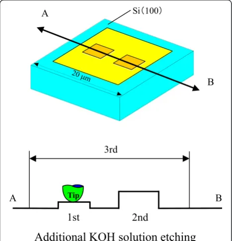
[image:2.595.58.290.88.369.2]The specimens were n-type Si (100) wafers. The samples were exposed in a clean atmosphere to allow their
Si(100)
Figure 1Mechanical pre-processing method.
A
B Si 100
1st
2nd
A B
Additional KOH solution etching
3rdTip
[image:2.595.305.539.468.711.2]surfaces to become covered with a natural oxide layer less than 2 nm thick. First, mechanical processing was performed using diamond tip sliding with an AFM under atmospheric conditions at room temperature and humidity ranging between 50% and 80%.
Dependence of KOH solution etching on load and scan density of mechanical pre-processing
We clarified the conditions under which the etching rate increased after mechanical pre-processing due to the removal of the natural oxide layer. To evaluate the dependence of the KOH solution etching of the mech-anically pre-processed area on the applied load and scanning density, diamond tips were directly slid on the
Si (100) using the AFM, and square areas were proc-essed as shown in Figure 1. The changes in the profiles of the processed areas were observed for a light applied load and an expanding scanning range. The Si (100) specimens were driven with the diamond tip at various load conditions. Scanning was performed 128, 256, and 512 times on a 4 × 4μm2area. To realize protuberance formation and plastic deformation, 100 ± 10 nm radius diamond tips were selected [23].
KOH solution etching of the pre-processed silicon sub-strate with 10 wt% KOH solution at 20°C ± 3°C was per-formed on the AFM apparatus. After etching, the specimen was washed with distilled water, and the profile changes caused by the etching were then evaluated at the
15
10
10
5 5
15 0
100 200
nm
m 20
20
(a)
(c) (b)
83.95 10.01
82.51
26.38
A A’
B B’
1 N
2 N
4 N
6 N
*Processing conditions
Number of samples: Left: 128 Processed area: 44 2
5.0
m
-100
0
10.0 15.0
0 nm
5.0
m
-100
100
0
10.0 15.0
0 nm
100
20.0
[image:3.595.71.538.273.717.2]20.0
same positions using the same diamond tip as the process-ing tool.
Dependence of additional KOH solution etching on etching time
Three types of mechanical pre-processing were per-formed, as shown in Figure 2. For the first and second, the silicon surfaces were processed at 10- and 40-μN load at 1 × 1 μm2, respectively. Diamond tip sliding at 10-μN load and 256 scanning number produced protu-berance. At 40-μN load, the processed area protuber-ated, and plastic deformation began [27,28]. Under these load conditions, the processed layers prevented KOH solu-tion etching. For the third type of pre-processing, the
sample was slid at 1.5-μN load and 256 scans in a 5 × 5μm2area. Finally, the processed samples were etched with 10 wt% KOH solution at 20°C ± 3°C for 10, 25, 30, and 40 min. Changes in the topography of the sample during the etching process were observed by tip scanning at less than 0.3μN over an area of 15 × 15μm2.
Results and discussion
Dependence of KOH solution etching on mechanical pre-processing owing to the removal of the natural oxide layer
To clarify the mechanism responsible for the increase in the etching rate on the removal of the natural oxide layer, the mechanical pre-processing was performed at
15
10
10
5 5
15 0
100 200
nm
m 20
20
50.48
1.526 50.40
82.51
(a)
(b)
(c)
A A’
B B’
1 N
2 N
4 N
6 N
*Processing conditions
Number of samples: Left: 256 Processed area: 44 2
2
5.0
m
-100
0
10.0 15.0
0
100
nm
5.0
m
-100
0
10.0 15.0
0
100
nm
20.0
[image:4.595.70.539.271.715.2]20.0
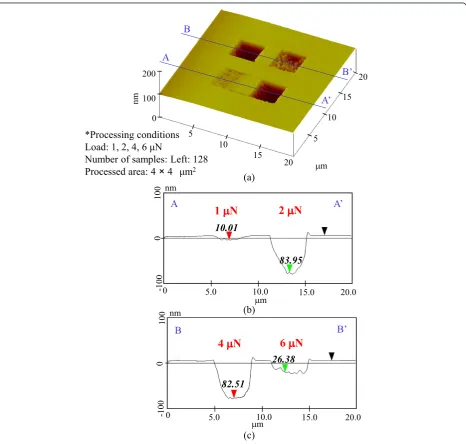
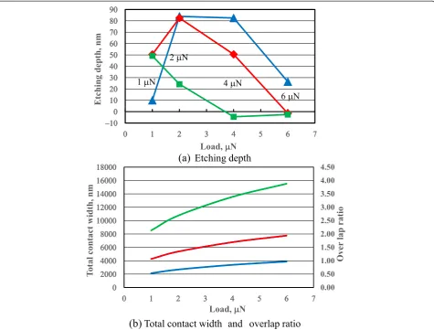
1-, 2-, 4-, and 6-μN load. The dependence of the etching profile on the pre-processing load at 128 scans is shown in Figure 3. The etching depths of the samples pre-processed at 1- and 2-μN load were 10 and 84 nm, respectively. At 4-μN load, the etching depth was satu-rated at 83 nm. However, the etching depth decreased to 26.3 nm at 6-μN load. Thus, the greatest etching depths were obtained at the 2- and 4-μN-load pre-processed areas.
Furthermore, for 256 scans, the etching depths were 50 nm at 1-μN load, 83 nm at 2-μN load, 50 nm at 4-μN load, and 0 nm at 6-μN load, as shown in Figure 4. The largest etching depth, 83 nm, was obtained in the areas pre-processed at 2-μN load. Figure 5 shows the etching
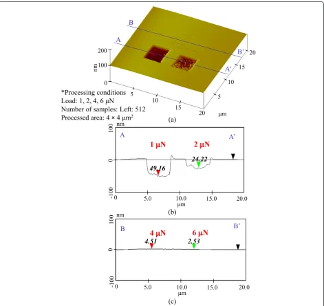
profiles of pre-processed areas scanned 512 times. The greatest etching depth obtained after 512 scans was 50 nm at the lowest load of 1μN.
Figure 6a shows the dependence of etching depth on the pre-processed load. Under these conditions, the un-processed areas were negligibly etched. A load range within which the etching depth increased existed for every scanning number, and these load ranges tended to increase as the number of scans decreased. The contact pressure and contact diameter were evaluated using the Hertzian equation. At 1 and 6μN, the contact pressures were 6.9 and 12.5 GPa, respectively.
The scanning density decreased with the scanning cycle number. The total contact sliding width can be
15
10
10
5 5
15 0
100 200
nm
m 20
20
4.51 2.53
49.16 24.22
(a)
(b)
(c)
A A’
B B’
1 N
2 N
4 N
6 N
*Processing conditions
Number of samples: Left: 512 Processed area: 4 2
5.0
m
-100
0
10.0 15.0
0
100
nm
5.0
m
-100
0
10.0 15.0
0
100
nm
20.0
[image:5.595.67.539.270.715.2]20.0
evaluated from the product of the contact diameter and scan number. Then, to evaluate the overlap ratio, the total contact width is divided by the scanning width. For example, at 6-μN load, the Hertzian contact diameter is nearly 30.3 nm; therefore, the total contact width for 128 scans was 30.3 × 128 nm and the overlap ratio was nearly 0.97, as shown in Figure 6b. In this case, the total contact width was smaller than the scanning width. The natural oxide layer formed on the Si surface was re-moved at low scan number conditions; overlap of the sliding contact area appeared to produce an etching-resistant layer.
Owing to the removal of the natural oxide layer, 512 scans at 1-μN load also increased the etching rate. Pro-cessing at higher loads of 4 and 6 μN increased the amount of mechanochemical oxidation owing to the high density of the scanning and thus decreased the etching depth. At 512 scans, the total contact width was larger than the scanning width, so the contact area over-lapped. Pre-processing at low load and scanning density efficiently removed the natural oxide layer by
mechanical action while also mechanochemically gener-ating a thin oxide layer because of the sliding overlap.
To clarify the etch properties of pre-processed areas at higher load, the etching profiles obtained at 8-, 10-, 15-, and 20-μN load after 256 scans were evaluated as shown in Figure 7. In these cases, etching grooves could not be de-tected in any of the processed areas. The heights of all of the processed areas were slightly greater than those of the unprocessed areas. Thus, the effect of any increases in etch-ing rate resultetch-ing from the removal of the natural oxide layer could not be obtained. This is conceivable because mechanochemical oxidization increases at higher load, resulting in improved resistance towards etching with KOH solution.
To compare the resistances of the natural oxide layer and the mechanochemically generated oxide layer to etching, we extended the etching time by 5 min. Figure 8 shows the etching profiles of pre-processed areas at 2-, 4-, 8-, and 15-μN loads. In this case, etching grooves were observed in pre-processed areas at 2 and 4 μN. In contrast, the heights of the pre-processed areas at 8 and
0.00 0.50 1.00 1.50 2.00 2.50 3.00 3.50 4.00 4.50
0 2000 4000 6000 8000 10000 12000 14000 16000 18000
0 1 2 3 4 5 6 7
Load, µN
−10 0 10 20 30 40 50 60 70 80
0 1 2 3 4 5 6 7
Etching depth,
nm
Load, µN
1µN
2µN
4µN
6µN
[image:6.595.61.537.89.450.2](a)
Etching depth
15 μN were higher than that of the unprocessed area. This is conceivable because the areas pre-processed at 8-and 15-μN load had better etching resistance towards KOH solution than that of the natural oxide layer. The etched sil-icon surfaces were very rough because the etching rate changed over different features on the surface, such as areas of damage, oxide, and adsorbates.
Therefore, with 256 scanning cycles, mechanical pre-processing at a load of 1 to 4 μN was effective in in-creasing the etching rate. Over 8-μN load, mechanical pre-processing was effective in forming an etch-resistant layer on the Si surface.
To clarify the mechanism of the mechanical removal and formation of this etch-resistant layer, the surface contact stress was evaluated using the boundary element method [27]. The dependences of the maximum principal and shear stresses on load were estimated for 100-nm-radius diamond tips. The 1- to 4-μN-load range corresponds to a contact pressure of 6.9 and 10.9 GPa. Therefore, it can be con-cluded that this contact pressure range is suitable for the removal of the natural oxide layer on a silicon surface at low-density scanning.
Silicon fractures under tensile stress at a certain load. In maximum tensile stress areas, silicon bond breakage
1.87 1.19
1.17 0.63
15
10
10
5 5
15
0
25 50
nm
μm 20
20
A A’
B B’
*Processing conditions Load: 8 ,10, 15, 20 μN Number of samples: Left: 256 Processed area: 44 μm2
8
µ
N
10
µ
N
15
µ
N
20
µ
N
(a)
(b)
(c)
5.0
µm
-250
0
10.0 15.0
0
250
nm
20.0
5.0
-250
0
10.0 15.0
0 nm
20.0
250
[image:7.595.66.538.86.540.2]µm
appears to stem from tensile stress caused by diamond tip friction [27]. Therefore, the reaction of silicon may take place at the rear edge of the sliding contact area where the elongation stress is the highest. At loads of over 8 μN, protuberance height increased rapidly at 13.8-GPa contact pressure and 1.8-GPa tensile stress. Therefore, this protuberance-related phenomenon oc-curred through a mechanochemical reaction where ad-sorbates, such as water and oxygen, reacted with the silicon. The local destruction of interatomic bonds seems to increase at over 6 μN because of the concen-trated stress and reaction of the newly formed surface
with surrounding materials. This boundary load that in-creases and dein-creases the etching depth is nearly 6 μN. At this load, the contact pressure and tensile stress are 12.5 and 1.5 GPa, respectively.
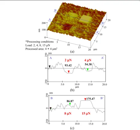
Additional KOH solution etching of processed protuberances with and without plastic deformation
As mechanical pre-processing, protuberances with and without plastic deformation were processed at 10- and 40-μN loads. It was found that less surface damage oc-curred than that due to plastic deformation during the nanoprocessing on Si. The shear stress was evaluated to
86.87 175.47 93.42 54.38
(a)
(b)
(c)
2
µµ
N
4
µ
N
8
µ
N
15
µ
N
A A’
B B’
0 100 200
nm
20 10
5
15
µm 15
10
5
20
5.0
µm
-250
0
10.0 15.0
0
250
nm
20.0
5.0
-250
0
10.0 15.0
0
250
nm
20.0 *Processing conditions
[image:8.595.71.538.89.524.2]Load: 2, 4, 8, 15 μN Processed area: 44 μm2
estimate the plastic deformation of the silicon, and the effect of the evaluated contact stress on protuberance height and groove depth was studied [27,28].
The presence of a mechanochemical local oxide layer prevented KOH solution etching. Protuberance heights increased until the tensile stress reached 4.5 GPa and then decreased with load. At this peak height, the max-imum shear stress attained was more than 8 GPa. This suggests that mechanochemical processing using a 100-nm-radius diamond tip is load dependent when the shear stress exceeds the strength of silicon, inducing a plastic deformation of several nanometers. Additional
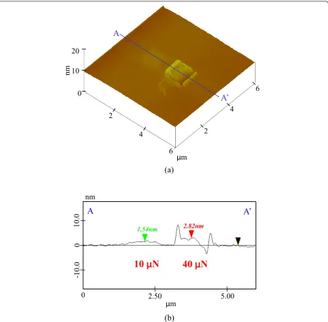
KOH solution etching was performed on the processed silicon to evaluate the chemical properties of the proc-essed area. The topography and cross-sectional profiles of a silicon sample pre-processed with a 100-nm-radius diamond tip at loads of 10 and 40 μN were obtained by scanning at 1.5μN over an area of 6 × 6μm2as shown in Figure 9. At 10-μN load, a 1.5-nm-high protuberance was mechanochemically generated by the sliding of the dia-mond tip. In contrast, at 40μN, the height of the protuber-ance reached 3 nm as shown in Figure 2, while plastic deformation produced a groove at the end of the scanning area. The natural oxide layer was removed under the
1.5-10
0
2
4
6
2
4
6
nm
µ
m
20
(a)
(b)
A
A’
1.54nm 2.82nm
A
A’
µ
m
-10.0
0
2.50
5.00
0
10.
0
nm
[image:9.595.65.538.249.713.2]10
µ
N
40
µ
N
μN load at 6 × 6μm2scanning area and 256 scanning cy-cles. At nearly 10-μN load, the 100-nm-radius tip produced protuberances of nearly 1.5 nm through silicon oxidation. However, the maximum shear stress increased beyond the yield criterion at nearly 40-μN load, resulting in silicon plastic deformation and a subsequent change in profile. In this condition, the height of the processed area was as much as 3 nm higher than that of the area processed at
10-μN load, and surface damages such as dislocations were in-creased in number.
To understand the dependence of the relative etching depth on etching time, the pre-processed and unpro-cessed areas were etched with KOH solution for 10, 15, 20, 25, 30, and 40 min. No significant change in the
topography of the surface was observed even after 10-and 15-min etching. The heights of the protuberances were slightly increased to 2.3 and 3.4 nm at 10 and 40
μN, respectively.
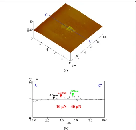
Figure 10 shows the topography and cross-sectional profiles of the processed surface after 20-min KOH etch-ing. The square groove of the 6 × 6μm2area processed at 1.5-μN load was slightly etched. Although the depth of this groove was 1 nm or less, the roughness of the processed surface was slightly increased. Meanwhile, the area pre-processed at 10 and 40μN was not etched.
[image:10.595.63.539.261.714.2]Figure 11 shows the etching profile of pre-processed areas after 25 min. The etching depth of the area pre-processed at 1.5-μN load was significantly increased to
more than 110 nm. This rapid increase in etching depth was due to the removal of the natural oxide layer by the low-load pre-processing. In contrast, the changes in the profiles of the areas pre-processed at 10 and 40μN, and the basal plane of the unprocessed areas, were very small. The natural oxide layer worked as an etching mask at 25 min. While the heights of the pre-processed areas were exactly the same as those before etching, the area pre-processed at 40-μN load was enlarged by the plastic deformation.
Figure 12 shows the topography and cross-sectional pro-files of the pre-processed areas after 30-min etching. The
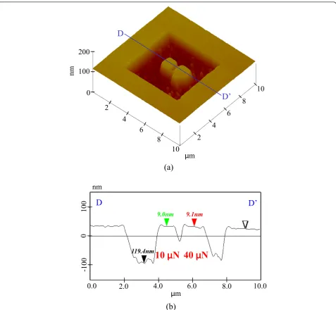
etching also advanced in the unprocessed area. The etching depth of the area processed at 1.5 μN progressively creased to 210 nm, while that of the unprocessed area in-creased to 140 nm. This implied that only the high-loaded processed area was not etched because of the mechano-chemical oxide layer. The height obtained at 10-μN load was slightly higher than that at 40-μN load.
Figure 13 shows the etching profile of pre-processed areas after 40-min etching. The etching depths of both the low-load processed and unprocessed areas were ap-proximately 530 nm. In contrast, the areas processed at high loads of 10 and 40 μN were not etched. This
100
0
2
6
8
2
6
10
nm
µ
m
200
4
10
4
8
D
D’
9.0nm 9.1nm
119.4nm
D
D’
µ
m
-100
0
nm
100
(a)
(b)
2.0
8.0
0.0
4.0
6.0
10.0
[image:11.595.60.538.272.712.2]10
µ
N 40
µ
N
experimentally confirmed that high-loaded processed protuberate areas show superior etching resistance to-wards KOH solution due to formation of a high-density oxide layer.
Figure 14 shows the dependence of relative etching depth on KOH solution etching time. The standard plane is the unprocessed area. The plane heights of the areas pre-processed at 10- and 40-μN load from the standard plane are denoted as A and B. The corre-sponding height of the area pre-processed at 1.5-μN load is C. Between 10 and 20 min, there was little change in the topography of each area. From 25- to 30-min etching, it was observed that the etched depths sig-nificantly increased in the 1.5-μN-load pre-processed
area. However, etching was hardly observed in the 10-and 40-μN-load pre-processed areas. Etching of the un-processed area was hardly observed until 25 min. After 30-min etching, the unprocessed area was progressively etched owing to the removal of the natural oxide layer.
From 35 to 40 min, the etching depths of both the un-processed and 1.5-μN-load pre-processed areas were lar-ger than those of the areas processed at higher load. The area mechanically pre-processed at higher load exhibited resistance to etching owing to mechanochemical oxida-tion layer formaoxida-tion.
The difference between the heights of the 10-μN uni-form protuberance and the 40-μN protuberance with plastic deformation can be evaluated as A-B. Without
250
0
5
15
10
nm
µ
m
500
10
5
15
E
E’
70.24nm
139.7nm 146.3nm
E
E’
µ
m
-250
0
nm
250
(a)
(b)
2.0
8.0
0.0
4.0
6.0
10.0
[image:12.595.65.539.87.526.2]10
µ
N 40
µ
N
etching, the height of the area pre-processed at 10-μN load was lower than that at 40μN. When the KOH solu-tion etching time was increased, A-B was nearly 3 nm until 20 min. The heights of the areas were similar in value at 25 min. In contrast, at 30- and 35-min etching time, the height of the 10-μN load area was higher than that at 40 μN. These results show that the etching rate of the area pre-processed at 40-μN load was larger than that at 10 μN. This is deduced to be because the area pre-processed with plastic deformation at 40-μN load was more easily etched due to damage compared with the uniform protuberance pre-processed at 10μN.
Figure 15 shows a model of etching depth dependence on KOH solution etching time for pre-processed areas. As shown in Figure 15b, with an increase of etching time, by the removal of the natural oxide layer, the
1.5-μN-load pre-processed area was etched at first. The etching rate increased with KOH solution etching time under processing at low load and scanning density.
However, as shown in Figure 15c, the two areas proc-essed at higher load and scan density were not etched because of their thick oxide layers. These thick oxide layers, which were mechanochemically formed on the areas processed at higher load, prevented the KOH
250
0
5
20
15
5
20
10
nm
µ
m
500
10
15
(a)
(b)
F
F’
535.5nm
539.9nm
14.3nm
F
F’
µ
m
-0.50
0
10.0
15.0
0
0.
50
µ
m
5.0
20.0
[image:13.595.63.539.89.532.2]10
µ
N 40
µ
N
solution etching and thereby decreased the etching rate. From these results, the etching rate is controllable by the removal of the natural oxide layer and direct oxida-tion by mechanical acoxida-tion. Grooves with various depths can be obtained using this etching rate control.
Conclusions
To realize the nanofabrication of a Si substrate, the etching depths obtained with KOH solution were con-trolled using mechanical pre-processing under various loads and scanning density conditions. Removal and formation of the oxide etching mask was performed on silicon surfaces using atomic force microscopy.
Areas mechanically pre-processed at 1- to 4-μN load exhibited an increased KOH solution etching rate due to the removal of the natural oxide layer by the mech-anical action. The dependence of etching depth on pre-processing load and scanning density was clarified. At every scanning density, there were certain load ranges within which the etching depth increased. In contrast,
protuberances with a thick oxide layer produced by mechanical pre-processing at higher load suppressed etching. This mechanochemical oxide layer had super-ior etching resistance to that of the natural oxide layer.
Protuberances were processed on the Si surfaces under stress conditions both lower and higher than that where plastic deformation occurs. These processed areas were hardly etched by the KOH solution. For pro-tuberances with plastic deformation, the damaged layers were more easily etched than those without plastic deformation. Protuberance formation without plastic deformation by mechanical pre-processing can realize less damaged mask patterning. Additionally, areas at pre-processed low load and scanning density were easily etched. This implies that the various profiles obtained were possibly fabricated by the changing load and scanning density of the mechanical pre-processing and by additional KOH solution etching. With the removal of the natural oxide layer and formation of a mechanochemi-cal oxide layer without plastic deformation, the etching
−200
−100
0
100
200
300
400
500
600
700
800
0
5
10
15
20
25
30
35
40
Rel
at
ive et
chi
n
g
dept
h,
nm
Etching time, min
40µN 10µN
1.5 µN
C
B
A
A−B
(A−B)× 100
40µN (B)
10µN (A)
[image:14.595.60.539.88.442.2]1.5 µN (C)
depth can be controlled by changing the etching time. This therefore allows us to fabricate low-damage grooves of vari-ous depths.
Competing interests
The authors declare that they have no competing interests.
Authors' contributions
SM carried out the nanofabrication studies, participated in the
nanoprocessing using atomic force microscopy, and drafted the manuscript. SY carried out and evaluated the Si nanoprocessing experiment and helped to draft the manuscript. All authors read and approved the final manuscript.
Acknowledgements
This research was performed with the help of our graduate students at Nippon Institute of Technology.
Received: 4 April 2014 Accepted: 17 May 2014 Published: 29 May 2014
References
1. Drexler KE:Nanosystems: Molecular Machinery, Manufacturing, and
Computation.New York: Wiley; 1992.
2. Marrian CRK:Technology of Proximal Probe Lithography.SPIE Optical Engineering: Bellingham; 1993.
3. Eigler DM, Schweizer EK:Positioning single atoms with a scanning tunneling microscope.Nature1990,344:524–526.
4. Mamin HJ, Rugar D:Thermomechanical writing with an atomic force microscope tip.Appl Phys Lett1992,61:1003–1005.
5. Dagata JA, Schneir J, Harary HH, Evans CJ, Postek MT, Bennett J:
Modification of hydrogen-passivated silicon by a scanning tunneling microscope operating in air.Appl Phys Lett1990,56(20):2001–2003. 6. Nagahara LA, Thundat T, Lindsay SM:Nanolithography on semiconductor
surfaces under an etching solution.Appl Phys Lett1990,57(3):270–272. 7. Heim M, Eschrich R, Hillebrand A, Knapp HF, Cevc G, Guckenberger R:
Scanning tunneling microscopy based on the conductivity of surface adsorbed water.J Vac Sci Technol B1996,14(2):1498–1502.
8. Miyake S:Atomic-scale wear properties of muscovite mica evaluated by scanning probe microscopy.App Phys Lett1994,65:980–982.
9. Miyake S:1 nm deep mechanical processing of muscovite mica by atomic force microscopy.App Phys Lett1995,67(20):2925–2927. (a)
(b)
(c)
1st 2nd
Removal of natural oxide layer
Natural oxide layer Tip
Tip
[image:15.595.57.539.89.493.2]Thick oxidized layer caused by KOH solution etching Damage layer
10. Miyake S, Ishii M, Otake T, Tsushima N:Nanometer-scale mechanical processing of muscovite mica by atomic force microscope.J Jpn Soc Prec Eng1997,63(3):426–430.
11. Miyake S, Otake T, Asano M:Mechanical processing of standard rulers with one-nanometer depth of muscovite mica using an atomic force microscope.J Jpn Soc Prec Eng1999,65(4):570–574.
12. Miyake S, Kim J:Nanoprocessing of carbon and boron nitride nanoperiod multilayer films.Jpn J Appl Phys2003,42(3B):L322–L325.
13. Miyake S, Matsuzaki K:Mechanical nanoprocessing of layered crystal structure materials by atomic force microscopy.Jpn J Appl Phys2002,
41(9):5706–5712.
14. Karaki T, Miyake S, Watanabe J:Facilitation mechanism of polishing rate in chemical polishing of Si single crystals: a study on mechano-chemical polishing (2nd report).J Jpn Soc Prec Eng1980,46(3):331–337. 15. Kaufman FB, Thompson DB, Broadie RE, Jaso MA, Guthrie WL, Pearson DJ,
Small MB:Chemical–mechanical polishing for fabricating patterned W metal features as chip interconnects.J Electrochem Soc1991,
138(11):3460–3465.
16. Miyake S, Nakata H, Watanabe J, Kuroda H:Face grinding of silicon wafer with resin bonded fine grained diamond wheel.J Jpn Soc Prec Eng1982,
48(9):1206–1212.
17. Lee HT, Oh JS, Park SJ, Ha JS, Park KH, Yu HJ, Koo JY:Nanometer-scale lithography on H-passivated Si (100) with an atomic force microscope in
air.J Vac Sci Tech A1997,15(3):1451–1454.
18. Chen L, Morita N, Ashida K:Maskless pattern formation which used alkaline etching and nano-scale cutting by using friction force microscope.J Jpn Soc Prec Eng2000,66:23–27.
19. Ashia K, Chen L, Morita N:New maskless micro-fabrication technique of single-crystal silicon using the combination of nanometer-scale machining and wet etching.InProceedings of the Second Euspen
International Conference: May 27–31 2001.Turin. Bedford: Euspen; 2001:78–81.
20. Yu BJ, Dong HS, Qian LM, Chen YF, Yu JX, Zhou ZR:Friction-induced nanofabrication on monocrystalline silicon.Nanotechnology2009,
20:303–465.
21. Guo J, Song CF, Li XY, Yu BJ, Dong HS, Qian LM, Zhou ZG:Fabrication mechanism of friction-induced selective etching on Si(100) surface.
Nanoscale Res Lett2012,7:152–161.
22. Yu BJ, Qian LM:Effect of crystal plane orientation on the friction-induced nanofabrication on monocrystalline silicon.Nanoscale Res Lett2013,
8:137–144.
23. Miyake S, Kim J:Microprotuberance processing of silicon by diamond tip scanning.J Jpn Soc Prec Eng1999,65(12):1788–1792.
24. Miyake S, Kim J:Nano protuberance and groove processing of silicon by diamond tip sliding.The Institute of Electrical Engineers of Japan:
Transactions on Sensors and Micromachines2000,120-E(7):350–356.
25. Miyake S, Kim J:Fabrication of silicon utilizing mechanochemical local oxidation by diamond tip sliding.Jpn J Appl Phys2001,40:L1247–L1249. Part 2, no. 11B.
26. Miyake S, Kim J:Increase and decrease of etching rate of silicon due to diamond tip sliding by changing scanning density.Jpn J Appl Phys2002,
41:L1116–L1119.
27. Kim J, Miyake S:Nanometer scale protuberance and groove processing of silicon by mechano-chemical action and its application of etching mask.
J Jpn Soc Prec Eng2002,68(5):695–699.
28. Miyake S, Kim J:Nanoprocessing of silicon by mechanochemical reaction using atomic force microscopy and additional potassium hydroxide solution etching.Nanotechnology2005,16:149–157.
29. Miyake S, Zheng H, Kim J, Wang M:Nanofabrication by mechanical and electrical processes using electrically conductive diamond tip.J Vac Sci
Tech B2008,26(5):1660–1665.
doi:10.1186/1556-276X-9-269
Cite this article as:Miyake and Yamazaki:Low-damage direct patterning of silicon oxide mask by mechanical processing.Nanoscale Research Letters20149:269.
Submit your manuscript to a
journal and benefi t from:
7Convenient online submission 7Rigorous peer review
7Immediate publication on acceptance 7Open access: articles freely available online 7High visibility within the fi eld
7Retaining the copyright to your article