International Research Journal of Engineering and Technology (IRJET)
e-ISSN: 2395 -0056 Volume: 03 Issue: 05 | May-2016 www.irjet.net p-ISSN: 2395-0072© 2016, IRJET | Impact Factor value: 4.45 | ISO 9001:2008 Certified Journal
| Page 2605
Design and Implementation of 32-bit ALU with 16 operations using
Reversible Logic Gates
DEEPA.G
1, MADHURI.E
2, MALASHREE.S
3, MAMATHA.K
4SUPRIYA.K.V
5UG Student, Department of Electronics and Communication Engineering, Dr.T.T.I.T, K.G.F, India1, 2, 3, 4. Assistant Professor, Department of Electronics and Communication Engineering, Dr.T.T.I.T, K.G.F, India5
---***---Abstract
-Reversible logic is one of the emerging technologies
having promising applications in quantum computing. This paper will deal with the design of a 32 bit reversible Arithmetic Logic Unit (ALU) with 16 operations is presented by making use of Double Peres gate, Fredkin gate, Toffoli gate, DKG gate and NOT gate. A new VLSI architecture for ALU using reversible logic gates is proposed.
ALU is one of the most important components of CPU that can be part of a programmable reversible computing device such as a quantum computer. A first single bit reversible ALU is designed and then 32 single bit ALU’s are cascaded together taking carry out of ALU performing LSB operation as an input to carry in of ALU performing next LSB operation. Design is implemented and verified in Xilinx.
Keywords- Low power ALU, Reversible gates, DPG, DKG,
Fredkin, Toffoli, Feynman.
I. INTRODUCTION
Now-a-days, the electronic systems are an integral part of a human’s life. As technology develops, the complexity of the system also increases. This gives rise to increase in power consumption, which is a great issue faced by the world today.
Energy dissipation due to information loss in high technology circuits and systems constructed using irreversible hardware was demonstrated by R. Landauer in the year 1960. According to Landauer’s [5] principle, the loss of one bit of information lost will dissipate kTln2 joules of energy where, k is the Boltzmann’s constant, T is the absolute temperature. In 1973, Bennett [6] showed that in order to avoid kTln2 joules of energy dissipation in a circuit it must be built from reversible circuits. Reversible circuits (gates) have the same number of inputs and outputs and there is a one to one mapping between vectors of inputs and outputs. Thus the vector of input states can be always uniquely reconstructed from the vector of output states.
1.1 The Arithmetic Logic Unit (ALU)
ALU is essentially the heart of a CPU. Different kinds of computers have different ALU’s but all of the ALU’s contain arithmetic unit and logic unit, which are the basic structures. This allows the computer to add, subtract, and to perform basic logical operations such as AND, OR etc.
1.2 Reversible Logic Gates
A function is reversible if each input vector produces a unique output vector. Reversible logic is of growing importance to many future computer technologies. It is not possible to realize quantum computing without implementation of reversible logic. The main purposes of designing reversible logic are to decrease quantum cost, depth of the circuits and the number of garbage outputs. The reversible circuits form the basic building block of quantum computers as all quantum operations are reversible. The two main constraints of reversible logic circuits are:-
[1] Fan-out not possible.
[2] Feedback or loops not allowed.
A reversible logic circuit should have the following salient features:
[1] Use minimum number of reversible gates.
[2] Use minimum number of garbage outputs.
[3] Use minimum number constant inputs.
1.2.1 NOT Gate
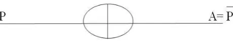
[image:1.595.321.551.594.638.2]The simplest Reversible gate is NOT gate and is a 1*1 gate. The Reversible 1*1 gate is NOT Gate with zero Quantum Cost is as shown in the Figure 1.1. If input is A then output is P=A
Figure 1.1: NOT Gate
1.2.2 FEYNMAN Gate
© 2016, IRJET | Impact Factor value: 4.45 | ISO 9001:2008 Certified Journal
| Page 2606
Figure 1.2: Feynman gate1.2.3 TOFFOLI Gate
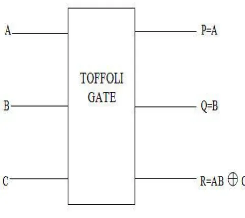
[image:2.595.36.544.67.302.2]Toffoli gate is a 3*3 gate 1with inputs (A, B, C) and outputs P=A, Q=B, R=AB XOR C. It has quantum cost of 5 and garbage outputs of 2. It is also called as CCNOT gate. It was invented by Tommaso Toffoli, is a universal reversible logic gate, which means that any reversible circuit can be constructed from Toffoli gates [6].
Figure 1.3: Toffoli gate
1.2.4 FREDKIN Gate
Fredkin gate which is a 3*3 gate with inputs (A, B, C) and outputs P=A, Q=A'B+AC, R=AB+A'C. It has Quantum cost 5 [6].
Figure 1.4: Fredkin gate
1.2.5 DPG Gate
[image:2.595.313.551.400.576.2]Double Peres gate which is a 4*4 gate having inputs (A, B, C) and outputs P = A;Q = A XOR B; R = AB XOR C.
Figure 1.5: Double Peres Gate
It has Quantum cost four. Some of the 3x3 gates are designed for implementing some important combinational functions in addition to the basic gates. If the input is A, B, C, D then output is P, Q, R, S.
1.2.6 DKG Gate
[image:2.595.45.286.453.667.2]International Research Journal of Engineering and Technology (IRJET)
e-ISSN: 2395 -0056 Volume: 03 Issue: 05 | May-2016 www.irjet.net p-ISSN: 2395-0072© 2016, IRJET | Impact Factor value: 4.45 | ISO 9001:2008 Certified Journal
| Page 2607
input A=1, then it works as a reversible Full subtractor. Its [image:3.595.313.567.95.472.2]Quantum cost is 6.
Figure 1.6: DKG Gate
II. LITERATURE SURVEY
Gordon. E. Moore in 1965 predicted that the numbers of components on the chip will double every 18 months. Initially he predicted only for 10 years but due to growth in the integrated circuit technology his prediction is valid till today
In the year 1994 Shor did a remarkable research work in creating an algorithm using reversibility for factorizing large number with better efficiency when compared to the classical computing theory. In 2010 Lihui Ni, Zhijin Guan, and Wenying Zhu described general approach to construct the Reversible full adder and can be extended to a variety of Reversible full adders with only two Reversible gates [4].
V. Rajmohan and Dr. V. Ranganathan implemented counters using reversible logic. The synchronous and asynchronous counter designs have the applications in building reversible ALU, reversible processor etc. This work forms an important move in construction of large and complex reversible sequential circuits for quantum computers [2].
III. PROPOSED WORK
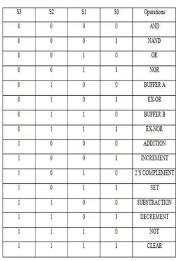
ALU has 2 parts, 1st which has Double Peres Gate as base of the circuit and is selected when select line s3 is zero. The operations performed here are buffer, AND, OR, NAND, NOR, EX-OR, and EX-NOR. 2nd part has DKG Gate as base of the circuit and is selected when select line s3 is one. The operations performed here are add, increment, 2’s complement, set, subtract, decrement, not, and clear. The operations selected depending on various select lines are shown in the table 3.1.
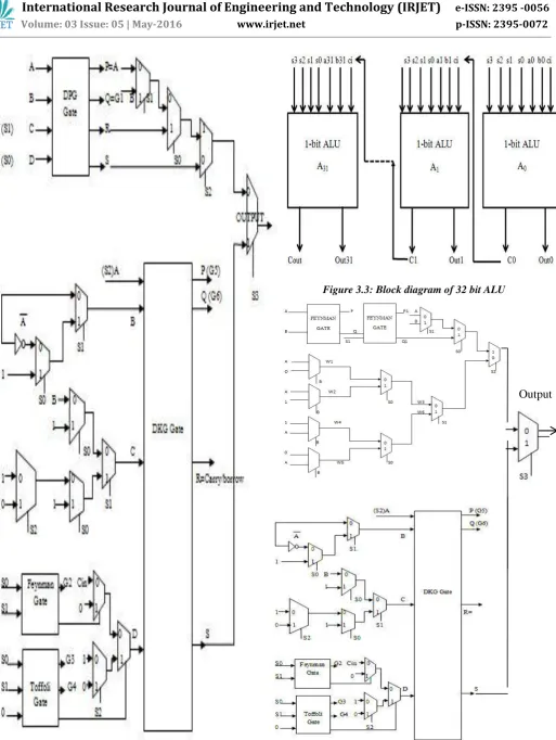
[image:3.595.58.267.142.335.2]The 2:1 Multiplexer is designed using Fredkin gate when we make A as select line and (B & C) as input. B orC is selected depending on A is 0 or 1 respectively. The block diagram is shown in figure 3.1.
Figure 3.1: 2x1 MUX
[image:3.595.311.556.549.688.2]© 2016, IRJET | Impact Factor value: 4.45 | ISO 9001:2008 Certified Journal
| Page 2608
Figure 3.2: Block diagram of One bit ALUFigure 3.3: Block diagram of 32 bit ALU
Figure 3.4: Block diagram of Modified One bit ALU
International Research Journal of Engineering and Technology (IRJET)
e-ISSN: 2395 -0056 Volume: 03 Issue: 05 | May-2016 www.irjet.net p-ISSN: 2395-0072© 2016, IRJET | Impact Factor value: 4.45 | ISO 9001:2008 Certified Journal
| Page 2609
IV. SIMULATION RESULT
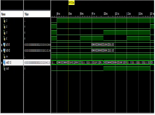
[image:5.595.65.560.62.467.2]The figure 4.1 shows the result for 1 bit ALU design for the input combinations 00, 01, 10 and 11.
Figure 4.1: Result for 1 bit ALU
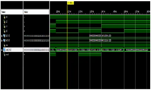
[image:5.595.36.297.157.314.2]The Figure 4.2 shows the result of first 4 operations (AND, NAND, OR and NOR). These operations are selected depending on select lines s3-s0 as shown in table 1.
Figure 4.2: Result for 1st 4-operations (AND, NAND, OR
and NOR)
Table 1
The Figure 4.3 shows the result of next 4 operations (BUFFER A, EX-OR, BUFFER B and EX-NOR). These operations are selected depending on select lines s3-s0 as shown in table 2.
Figure 4.3: Result for 2nd 4-operations (BUFFER A,
[image:5.595.316.552.342.441.2]EX-OR, BUFFER B and EX-NOR)
Table 2
The Figure 4.4 shows the result of next 4 operations (ADD, INCREMENT, 2’S COMPLEMENT and SET) these operations are selected depending on select lines s3-s0 as shown in table 3.
Figure 4.4: Result for 3rd 4-operations (ADD,
[image:5.595.37.289.388.509.2] [image:5.595.308.559.515.701.2]© 2016, IRJET | Impact Factor value: 4.45 | ISO 9001:2008 Certified Journal
| Page 2610
Table 3 [image:6.595.36.289.327.476.2]The Figure 4.5 shows the result of next 4 operations (SUBSTRACTION, DECREMENT A, NOT and CLEAR) these operations are selected depending on select lines s3-s0 as shown in table 4.
Figure 4.5: Result for 4th 4-operations (SUBSTRACTION,
DECREMENT A, NOT and CLEAR)
Table 4
V. CONCLUSION
In the present paper the proposed 32-bit ALU is designed using reversible logic gates such as Double Peres gate, DKG gate, Toffoli gate, Feynman gate. The multiplexers are designed using Fredkin gate. The main aim of the design in this paper is to improve the ALU.
Parameters
32-Bit ALU
32-Bit
Modified
ALU
Power
166.38mW
42.38mW
Delay
44.312ns
40.512ns
Levels of
logic
68%
67%
VI. BIBLIOGRAPHY
[1] C. H. Bennett, “Logical reversibility of computation”,
IBM J. Research and Development, 17, pp. 525 – 532, November1973.
[2] Feynman, R., “Quantum mechanical computers”
Optics, News, and pp.: 11-20 11, 1985.
[3] Fredkin, E. and T. Toffolli, “Conservative logic”, Intl.
J. Theoretical Phy., 21, pp.: 219-253, 1982.
[4] Lihui Ni, Zhijin Guan, and Wenying Zhu, “A General
Method of Constructing the Reversible Full-Adder”,
Third International Symposium on Intelligent Information Technology and Security Informatics, pp.109-113, 2010 5
[5] R. Landauer, “Irreversibility and heat generation in
the computing process”, IBM J. Research and Development, 5(3), pp.: 183-191, 1961.
[6] Toffoli T, “Reversible computing”, Technical Memo