2018 3rd International Conference on Computational Modeling, Simulation and Applied Mathematics (CMSAM 2018) ISBN: 978-1-60595-035-8
A Method of Camera Link Image Data Processing Based on FPGA
Shi-feng WANG
No. 50. Yongding Road, Haidian District, Beijing, China
Keywords: Camera Link image, Data processing, FPGA.
Abstract. Camera Link is based on the development of Channel Link Technology. The data is transmitted using low voltage differential signal (LVDS). It has some advantages, such as fast speed, strong anti-interference ability and so on. Camera Link is widely used in the field of robot vision applications. FPGA integrates rich gate circuit resources and has the advantages of high speed, which makes it suitable for processing parallel data. In this paper, a Camera Link image data processing method based on FPGA is proposed, which is verified by simulation and has been successfully applied to practical projects.
Introduction
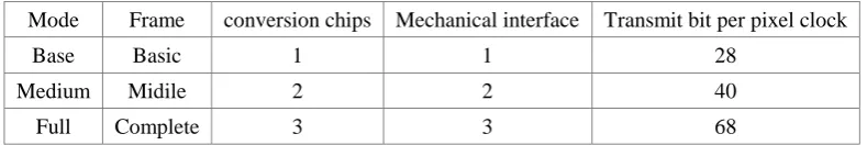
[image:1.595.101.496.479.545.2]Camera Link is a serial communication protocol in the field of machine vision application. It is based on the development of Channel Link technology and uses low voltage differential signal LVDS transmission. There are four kinds of camera signals: power signals, video data signals, camera control signals and serial communication signals. The video data signals are the core of Camera Link, including 1 pairs of differential clock and 4 pairs of serial differential data. The Camera Link conversion chip converts 4 pairs of differential data into parallel data, and parallel data includes 24 bit data, frame synchronization, row synchronization, data synchronization and image pixel clock. There are three modes of video transmission: Base, Medium and Full. The conversion chips, interfaces and data bits for each pixel clock transmission under the three modes are shown in the following table.
Table 1. Three modesTable headings.
Mode Frame conversion chips Mechanical interface Transmit bit per pixel clock
Base Basic 1 1 28
Medium Midile 2 2 40
Full Complete 3 3 68
FPGA (Field Programmable Gate Array) is a chip that can change the internal routing and logic by programming. It integrates logic block, layout and routing resources, configurable IO port, clock management unit, RAM memory, DSP module and other resources. It is widely used in video image preprocessing because of its fast processing speed and high capability of data processing in parallel.
The data output of Camera Link is in parallel, and FPGA stores the data in the FIFO, the processor reads the data out by detecting the state of FIFO, and then processes, displays, or compares the data.
System Structure
Peripheral
DATA1_P DATA1_N DATA2_P DATA2_N DATA3_P DATA3_N DATA4_P DATA4_N
CLK_P CLK_N
Camera Link Conversion
chip
DATA[23..0]
FVAL LVAL
DVAL
CLK_OUT
FPGA DSP
[image:2.595.135.464.75.181.2]Data Address Control
Figure 1. System constitution.
Chip Selection
We choose the DS90CR286A of National Semiconductor as the Camera Link convert chip. The chip can convert 4 serial LVDS signals to 28 bit parallel TTL data output, and the pixel clock can reach 66MHz.
We choose the XC7A200T-1FBG676I of Xilinx as the FPGA, which has 215k logic unit, 13Mb RAM block and 500 programmable IO ports. It has the advantages of low power consumption and fast speed, and can realize serial and parallel conversion of video signals.
Besides, we use DSP of TI as processor. The capacity of FIFO is small, so the DSP will read the data out when the data in the FIFO reaches a specified number. The DSP will receive a interrupt signal and calculate and display a frame of data according to the number of rows and columns when a frame of data is transmit.
Signal Connections
The signal of the system peripheral to the converter chip is 4 pairs of LVDS data plus 1 LVDS clocks. The rate range of the data line is 140~462Mbps, the clock frequency range is 20~66MHz. In this design, the pixel clock is 30MHz.
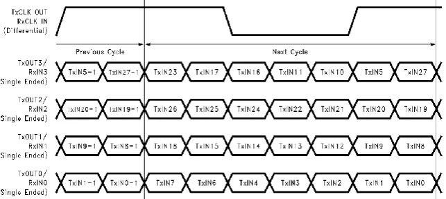
The DS90CR286A chip converts serial data to parallel data to FPGA, and the output data includes 24 bit data, FVAL (frame synchronization signal), LVAL (line synchronization signal), DVAL (data effective signal), and CLK_OUT (pixel clock). The correspondence of 4 LVDS serial data converting to parallel data are shown in the following figure.
The data transmission between DSP and FPGA are through EMIF bus, including control bus, address bus and data bus.
Figure 2. Correspondence of the serial and parallel data.
FPGA Design
Timing
[image:2.595.137.459.534.678.2]and the CLK_OUT is the pixel clock signal. The convert chip outputs data on the falling edge of the clock, and FPGA locks data on the data bus on the rising edge of the clock. It contains 640 clock cycles each row, and 480 rows each frame.
CLK_OUT LVAL
640 CLK_OUT周期
FVAL
480个LVAL
[image:3.595.88.499.117.176.2]LVAL
Figure 3. Timing of the Camera Link convert chip.
FPGA Code
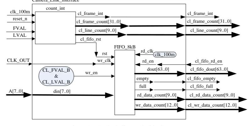
[image:3.595.88.512.260.506.2]The signals of Camera Link interface module are shown in table 2.
Table 2. The signals of Camera Link interface module.
Name I/O Bit width Meaning others
clk_100m I 1 Clock 100MHz
reset_n I 1 Reset Active low
FVAL I 1 frame synchronization Active high
LVAL I 1 line synchronization Active high
CLK_OUT I 1 pixel clock 30MHz
A I 8 parallel data in
cl_frame_int O 1 frame finish int
cl_frame_count O 32 frame count
cl_line_count O 10 line count
cl_fifo_rd_en I 1 fifo read enable Active high
cl_fifo_dout O 64 fifo data output
cl_fifo_empty O 1 fifo empty Active high
cl_fifo_full O 1 fifo full Active high
cl_rd_data_count O 10 fifo read time count
cl_wr_data_count O 13 fifo write time count
FVAL, LVAL, CLK_OUT and A[7..0] are the output signals of the conversion chip, and the timing is show in figure 3 .Other signals are connected to other modules inside the FPGA.
[image:3.595.95.495.555.757.2]FVAL LVAL CLK_OUT clk_100m reset_n count_int FIFO_8kB rst wr_clk wr_en din[7..0] rd_clk rd_en dout[63..0] empty full rd_data_count[9..0] wr_data_count[12..0] cl_frame_int cl_frame_count[31..0] cl_line_count[9..0] cl_fifo_rd_en cl_fifo_dout[63..0] cl_fifo_empty cl_fifo_full cl_rd_data_count[9..0] cl_wr_data_count[12..0] cl_frame_int cl_frame_count[31..0] cl_line_count[9..0] Camera_Link_interface clk_100m CL_FVAL_B & CL_LVAL_B cl_fifo_rst A[7..0]
Figure 4. The block diagram inside the FPGA.
The module generates the interrupt signal, the reset signal and the counting signals. The input signals are clock of 100MHz, reset signal, frame synchronization signal, the row synchronization signal. There are four output signals. The cl_frame_int signal is interrupt signal after the completion of transmission of one frame. It is low in usual state, when the falling edge of FVAL is detected, the cl_frame_int signal goes high for 8 clock as the interrupt for DSP. The DSP reads the data out and processes the data when the DSP receives the interrupt signal. The signal cl_frame_count is count for frame, it increases for one when the falling edge of FVAL is detected. The signal cl_line_count is the count for line, it increases for one when the falling edge of FVAL is detected. The signal cl_fifo_rst is the reset signal of the FIFO, which is active high. The signal goes high for one clock to reset the FIFO in order to clear the old data when the falling edge of FVAL is detected.
The FIFO solves the problem of the clock domain crossing. The data goes into FIFO with the pixel clock first, and then the data is read in the clock domain of 100MHz. The signal rst is the reset signal of the FIFO, which is generated by the module count_int, and it reset the FIFO at the beginning of every frame. The signal wr_en is the result of the AND operation of FVAL and LVAL. The signal wr_clk is the pixel clock. The signal din[7..0] is the output data A[7..0] of the conversion chip. The signal rd_clk is the main clock of FPGA, which is 100MHz. The others signals, including rd_en, dout[63..0], empty, full, rd_data_count[9..0], wr_data_count[9..0], are connected to the other modules in FPGA.
Simulation and Application
Simulation
[image:4.595.124.474.421.775.2]The simulation of the program is done to verify the function. The waveform of the signals cl_fifo_rst, cl_line_count[9..0], cl_frame_int, cl_frame_count[31..0] are shown in the following figures.
Figure 5. The waveform of signal cl_fifo_rst.
Figure 6. The waveform of signal cl_line_count[9..0].
Figure 8. The waveform of signal cl_frame_count[31..0].
Application
The method is used in the project. The infrared camera of 640*480 pixel is used as peripheral, and the cup full of hot water as the observed object. The output signals are divided into two, and one goes to the standard test instrument, and the other goes to the system. The connection diagram of the
instruments is shown in figure 9 and the result is shown in figure 10.
Cup
Infrared camera 640*480
Standard Instrument
The FPGA+DSP system
Figure 9. The connection diagram of the instruments.
Figure 10. The image comparison between the standard instrument and the system.
The system can implement the function of data processing and storage of Camera Link interface according to the result shown in figure 10.
Summary
A method of data processing of Camera Link based on FPGA is put forward in this article. The image data is converted form serial to parallel and stored in FIFO of FPGA, the DSP read the data out and process the data. The method has a certain application value in engineering practice.
References
[1] Xiaoyang Wang, Huixin Zhang, Qian Yang, Yongsheng Sun, Design of Camera Link protocol and FPGA digital image signal source, J. Network and Communication Engineering. 7 (2008) 59-61.
[2] Yanbin Chen, Gang Jin, Design of DSP+FPGA high speed real-time digital image processing system based on Camera Link standard, J. Modern scientific instruments. 6(2010) 61-63.
[3] Chunping Peng, L.B. Adams, An image acquisition and processing system based on Camera Link interface. J. Electronic design and Application. 3(2009).
[image:5.595.127.468.341.471.2][5] Ning Li, Junfa Wang, High speed data acquisition system based on Camera Link. J. Infra-red. 7(2005) 32-39.

![Figure 8. The waveform of signal cl_frame_count[31..0].](https://thumb-us.123doks.com/thumbv2/123dok_us/263959.1026574/5.595.127.468.341.471/figure-the-waveform-of-signal-cl-frame-count.webp)
