www.arpnjournals.com
POWER SHARING ANALYSIS OF A NEW MODIFIED MULTI-INPUT
INTERLEAVED BOOST CONVERTER BASED ON H-BRIDGE CELLS
Y.M. Buswig, W.M. Utomo,Z A. Haron, and A.A Bakar
Department of Electrical Power Engineering, Faculty of Electrical and Electronic Engineering, University Tun Hussein Onn Malaysia, 86400 Parit Raja, Batu Pahat, Johor, Malaysia.
E-mail: [email protected]
ABSTRACT
In this paper, a new modified multi-input boost converter is proposed using H-bridge cells as building blocks and uncoupled inductors in parallel using interleaved technique as ripple reduction method. The objectives of this paper are to design a high ripple reduction and a high-performance multi-input boost converter. Different operating modes and the switch realization of the new converter are obtained. The modes of operation based on the status of the four switches. The proposed multi-input boost converter is composed of two inputs source that accommodated with some extra semiconductors, inductances and diodes to form the interleaving technique as proposed method. The proposed concept has been investigated through simulation using the MATLAB/Simulink environment. The simulation results confirm the validity of the proposed method, which can be seen as a promising new topology that ensure multi-input converter suitable for renewable energy applications.
Keywords: Multi-Input Converter Interleaving Technique H-bridge Cells
INTRODUCTION
Nowadays, Multiple-input DC-DC converters are playing a significant role in interfacing and diversification of different energy sources. The single DC-DC converters are connected to electric sources like battery, fuel cell, wind power and other renewable energy with (V-I) features and the outputs can be combined with dc bus in both parallel or series (Valenciaga and Puleston, 2005) , (Kumar and Ikkurti, 2011), (Wang and Nehrir, 2008), (Jiang and Fahimi, 2011), (Dobbs and Chapman, 2003).
Therefore, several energy sources can be consolidated either in parallel (Tao et al, 2006)(Gummi and Ferdowsi 2010)(Chen et al. 2006) or in series(Ahmadi & Ferdowsi,2012),(Kumar and Jain, 2012), (Nami et al. 2010)(Shen and Yang, 2013) with the electric connected multiple-input converter topologies. However, the main restrictions of the input source topologies connected in parallel are the compulsory of the input voltage source to be asymmetrical and at one time, only one input source can provide energy to the load to obviate energy from the conjugation effect.
Series connecting the input sources are necessary to provide energy simultaneously. Therefore, in series configurations, by using an individual diode, each input source can avoid the other input source to form a parallel connection, which increases numbers of components (Ahmadi et al. 2013)(Li et al. 2010)(Kwasinski, 2009).
Nevertheless, these configurations have weaknesses such as expensive, huge and complicated in design. It also minimizes the efficiency and accuracy of the whole system. Consequently, a single converter with multiple inputs has been introduced, replacing the multiple single input converters.
Multiple-input converters offer uncomplicated and more consolidated styling as well as reducing cost and the systems complexity. Moreover, the efficiency of power distribution reinforces reliability at the regulated output voltage (Dobbs and Chapman 2003) (Tao et al. 2006).
Various isolated and non-isolated topologies on multiple-input converters have been presented (Tao et al.
2006) (Chen et al. 2002) (Patra et al. 2012) (Liu and Chen 2009). Electric-connected circuits belong to the non-isolated topologies while the magnetic-connected circuit belongs to those isolated topologies.
In the magnetic-connected circuit, the energy conversion transformation from sources to load is executed using flux technique and the time domain multiplexing (Matsuo et al. 1993). Thence, the necessity of the extra Peripheral circuitry and the transformer requirement make the magnetic-connected circuit complicated, huge, and expensive as well as increasing the circuit parameters dependency(Dobbs and Chapman, 2003)(Zhao et al. 2008)(Khaligh et al. 2009) while electric-connected circuit has a modular structure, reduces cost and is not using transformer, thus making this non-isolated circuit more attractive and greatly reduces the matter associated with magnetic-connected circuit..
PROPOSED MODIFICATION FOR MULTI-INPUT BOOST DC-DC CONVERTER
The operation principle of multi-input DC-DC converter is based on the essential of DC-DC converter. The essential operation of the basic DC-DC converter is to charge the passive elements of the converter during a specific period of time and then discharge the stored energy of the passive element through load during the remaining period of time over a single switching cycle. In the single-input DC-DC converter, power flow from single-input source to the load can be controlled by controlling charging and discharging of the inductor.
Similarly, in multi-input DC-DC converters, the inductors can be charged by multiple input voltage sources instead of one source depend on a suitable switching technique that connects or disconnects multiple-input sources to the inductor individually or simultaneously.
building blocks with uncoupled inductors in parallel using interleaved technique as ripple reduction are proposed in boost operation mode in order to reduce the ripple of input current as well as output current, and increase performance of the proposed multi-input converter system.
A simple outline of the proposed modified multi-input interleaved boost DC-DC converter using H-bridge cells with interleaving technique is shown in Figure 1.
Figure 1: Outline of a proposed modified multi-input interleaved boost DC-DC converter
DERIVATION OF THE PROPOSED MULTI-INPUT CONVERTER USING H-BRIDGE CELL
[image:2.612.320.551.49.250.2]Topology introduced in Figure 1 hereafter named multi-input interleaved boost DC-DC converter, resembles the topology of an interleaved boost converter with two inputs voltage sources. By replacing H-bridge cells in proposed converter with their circuit topology, one would obtain Figure 2. Four modes of operation that occur under unidirectional power flow are depicted in Figure 3 up to Figure 6.
V S1
i S1
S
8
-
+
V
2V
1
i S5
V
S2-
+
S
3
S
2
V L2
+ -
i
S2
+
-VL1 S
11
S
12
i L
+
-VO R C S10 S
9
i
L1 iL2
i
S6
-
+
S6S
5
V S5
S
7
S
4
V
S6 S1
-
+
[image:2.612.73.303.172.301.2]i O
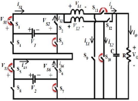
Figure 2:The schematic circuit of the proposed multi-input converter using cascaded H-bridge cells.
Mode 1- (S1,S3, S6,S7, S9& S12: on)
[image:2.612.317.548.351.521.2]In this mode, input source V1 supplies the energy to the load and inductor L2 while inductor L1 starts charging. Thus, the source V1 can operate individually as depicted in Figure-3
Figure 3: Derivation circuit of the mode 1
Mode 2- (S1, S3, S5, S7, S10& S11: on)
In this mode both of input sources (V1 and V2) supply the energy to the load and inductor L1, while inductor L2 starts charging. Thus, both the sources can operate simultaneously as depicted in Figure 4.
Figure 4: Derivation circuit of the mode 2
Mode 3- (S1, S3, S5, S7, S9 & S12: on)
[image:2.612.71.287.447.611.2]S3 S2
∆IL1
∆IL2
S4
Time
d1
d3
d4 d4
d2
d3 d2
d3
d4 d1
T3,4 S1
State of switches
Inductor s current
A V 1
L1
V2
L2
t2 t4 t5
V1+V 2
L2
V1+V 2
L1 t3 t1
[image:3.612.71.298.68.240.2]IIN=IL1+IL2 Figure 5: Derivation circuit of the mode 3
Mode 4- (S2, S3, S5, S7, S10 & S11: on)
In this mode, input source V2 supplies the energy to the load and inductor L1 while inductor L2 starts charging. Thus, the source V2 can operate individually as depicted in Figure 6.
Figure 6: Derivation circuit of the mode 4
SWITCH INVESTIGATION OF THE PROPOSED MULTI-INPUT CONVERTER
As a result of operation modes circuits of the proposed converter that in the unidirectional power flow, switches S4 and S8 are not used at all so they can be eliminated from the circuit. Also switches S3 and S7 are always on so they can be shorted. Residual switches S1, S2, S5, and S6 can be replaced by diodes or transistors considering the following explanation. If the power flows through the inductors are considered to be unidirectional, IL1and IL2is always positive.
As switch S2 conducts positive current and opposes negative voltage, it can be replaced by a diode D1 and as switch S1 conducts positive current and positive voltage it can be replaced by a transistor. Similarly, S6 can be replaced by a diode D2, and S5 can be replaced by a transistor. As switches S9 and S10 conduct positive current and positive voltage they can be replaced by transistors.
[image:3.612.317.537.116.252.2]Also, as switch S11 and S12 conduct positive current and opposes negative voltage it can be replaced by a diode D3 and D4 respectively. So the final circuit that is obtained is shown in Figure-7.
Figure 7:Final derived circuit of the proposed multi-input converter using cascaded H-bridge cells
OPERATING PRINCIPLE OF THE PROPOSED MULTI-INPUT DC-DC CONVERTER
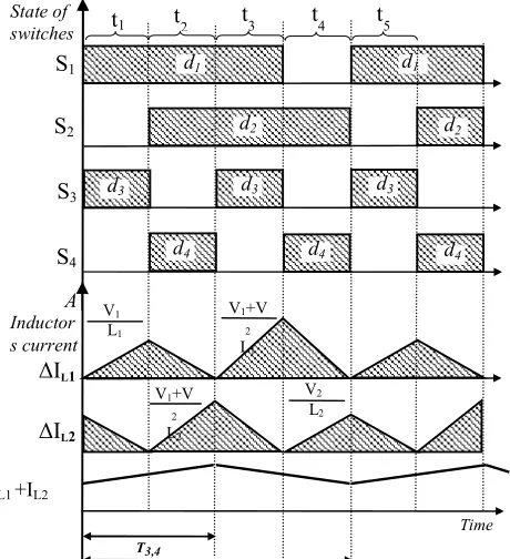
The gate pulses of the switches for the proposed multi-input converter have been purposely assumed that the duty cycle of S1, S2, S3 and S4 denoted as d1, d2, d3, and d4 respectively. The pulse modulation of the switches and change in inductors current waveforms of proposed multi-input converter are shown in Figure 8. Where T3,4represents the switching frequency of interleaving switches S3 and S4.
[image:3.612.71.296.326.500.2] [image:3.612.318.548.427.679.2]The switching conditions in different operations modes are shown in Figure9 up to Figure 12, and described as follow:
Equivalent circuit of mode 1
Referring to the Figure-9, during T1, the inductor current, and the capacitor voltage during T1 can be computed as given in equations (1), (2), and (3):
D4
S3 S4 D1
D2 S2
L2
+
V1
V2
L1
C
+
D3
S1
- L
O A D
Figure 9: Operating mode-1 at time T1.
1 1 1
L V dt diL
= (1)
2 2
1 2
L V L V dt
diL = − C (2)
RC
V C I dt
dV C = L2 − O (3)
Equivalent circuit of mode 2
Referring to the Figure-10, during T2, the inductor current, and the capacitor voltage during T2 can be computed as given in equations (4), (5), and (6):
Figure 10: Operating mode-2 at time T2.
1 1
2 1
1 ( )
L V L
V V dt
diL = + − C (4)
2
2 1
2 ( )
L V V dt
diL = + (5)
RC
V C I dt
dVC = L1 − O
(6)
Equivalent circuit for mode 3
Referring to the Figure 11, during T3, the inductor current, and the capacitor voltage during T3 can be computed as given in equations (7), (8), and (9):
Figure 11:Operating mode-3 at time T3.
2 2
2 1
2 ( )
L V
L V V
dt
diL C
− +
= (7)
1
2 1
1 ( )
L V V dt
diL = + (8)
RC
V C I dt
dVC = L2 − O
(9)
Equivalent circuit for mode 4
Referring to the Figure 12, during T4, the inductor current, and the capacitor voltage during T4 can be computed as given in equations (10), (11), and (12):
Figure 12:Operating mode-4 at time T4.
2
2 2
L V dt
diL = (10)
1 1
2 1
L V L V dt
diL = − C (11)
RC
V C I dt
dVC = L1 − O (12)
VOLTAGE TRANSFER RATIO OF THE PROPOSED MULTI-INPUT CONVERTER
Explained analysis for boost mode of operation is carried out in continuous conduction mode (CCM) under steady-state condition. In the analysis, switching loss and a resistive drop of passive components are considered to be negligible.
1 3 3
t = t = d
2 4 4
t = t = d
1 2 3 1
t + t + t = d
2 3 4 2
t + t + t = d
Where T represents the time period of the switching patterns as expressed in equation (13)
(13)
According to the volt-second balance theory, average inductor voltage over a single switching period should be zero:- 0 0 T i L L t d
Average inductor voltage L
d
v
=
∫
= = (14)
Assume that the current waveforms had reached a steady state condition. Thus, by analyzing the waveforms for IL1 and IL2 of the switching cycle for different working states based on Figure 8, can be written the following equations:-
1 1 1 2 3 1 2 2 3
1 2 3 4
1 1 1 1 1 1
( ) 1 ( ) 1
( ) ( ) ( ) ( )
0
2 2
iL O O
t
d V V V V d V V V V d
t t t t
d L L L L L L
− −
+ +
= + − + + − =
(15)
2 1 4 1 2 1 2 4 2
1 2 3 4
2 2 2 2 2 2
( ) ( )
( ) 1 ( ) ( ) 1 ( )
0
2 2
iL O O
t
d V V d V V V V V d V
t t t t
d L L L L L L
− + + −
= − + + − + =
(16)
(17)
3 3
1 1 2 1 2 2
1 2 3 4
1 1 1 1 1 1
1 4 1 2 1 2 4 2
1 2 3 4
2 2 2 2 2 2
( ) 1 ( ) 1
( ) ( ) ( ) ( )
2 2
( ) ( )
( ) 1 ( ) ( ) 1 ( )
0
2 2
i L total O O
t
O O
d V V V V d V V V V d
t t t t
d L L L L L L
V V
V d V V V V d V
t t t t
L L L L L L
− − + + = + − + + − − + + − + − + + − + =
(18)
In principle, equations (15)-(18) can be solved to find Vout. Even so, in order to simplify the calculation, it is assumed that L1=L2=L and d3=d4=d3,4. After some algebraic manipulations and solving equation derived from (18). The expression of the output voltage of the proposed multi-input converter shown as the in equation (19)
1 1 2 2
3 .4
(1 9 )
(1 )
O u t
V d V d
V d + = − SIMULATION RESULTS
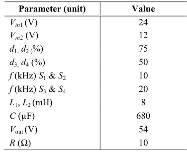
A multi-input converter with double inductance interleaved scheme has been considered for the simulation study in boost operation mode. A simulation model of the proposed converter using MATLAB Simulink is shown in Figure 13. All the results have been analyzed for matched sources and mismatched sources with continuous current mode under steady condition. A fixed frequency switching strategy had been selected to present the results of the simulation study. All the simulation parameters are given in Table-1.
[image:5.612.80.225.67.147.2]Figure 13: Simulation model circuit of proposed multi-input interleaved boost converter
Table-1 Powerstage parameters of the designed converter
Parameter (unit) Value
Vin1 (V) 24
Vin2 (V) 12
d1,d2 (%) 75
d3, d4 (%) 50
f (kHz) S1 & S2 10 f (kHz) S3 & S4 20
L1, L2 (mH) 8
C (µF) 680
Vout (V) 54
R (Ω) 10
Simulation results of switching signals, inductors voltage , inductors currents, input voltage sources and output voltage for boost mode of operation in case mismatched sources when voltage sources Vin1=24V and Vin2= 12V are shown in Figure14 up to Figure 17.
1 2 3 4
t + + + =t t t T
0 2
1+ = =
t total L i t L i t L i d d d d d d L2 D1 D2 D3 D4 L1
C R Load
[image:5.612.334.522.431.584.2]0.201 0.2011 0.2012 0.2013 0.2014 -1
0 1 2
S
3
0.201 0.2011 0.2012 0.2013 0.2014
-1 0 1 2
Time
S
4
0.201 0.2011 0.2012 0.2013 0.2014
-1 0 1 2
S
1
Iout
0.201 0.2011 0.2012 0.2013 0.2014
-1 0 1 2
S
[image:6.612.300.549.51.286.2]2
Figure 14: Switching signals of switches S1, S2, S3 and S4; [d1 = d2
=0.75; d3 =d4 = 0.5]
0.201 0.2011 0.2012 0.2013 0.2014
-50 0 50
V
L
2
0.201 0.2011 0.2012 0.2013 0.2014
4.6 4.8 5 5.2
IL
1
0.201 0.2011 0.2012 0.2013 0.2014
4.6 4.8 5 5.2
Time
IL
2
0.201 0.2011 0.2012 0.2013 0.2014
-50 0 50
V
L
1
Iout
Figure 15: Inductors voltage (VL1 and VL2) ;Switching signals of
switches S3 and S4 ;[d3 = d4 = 0.5]
As shown in Figure 15, the simulation results when the input voltage sources are mismatched: at time (t1), the inductor L1 was charged by 24V (i.e. VL1=V1) when the inductor L2 was discharged (i.e. VL2= V1–VO) and for time (t2), the inductor L2 was charged by 36 V (i.e. VL2 = V1+V2) when the inductor L1 was discharged (i.e. VL1=V1+V2 –VO) ; for time period (t3) the inductor L1 was charged by 36 V(i.e. VL1=V1+V2) when the 'inductor L2 was discharged (i.e. VL2=V1 + V2 –VO), and for time (t4) the inductor L2 was charged by 12 V (i.e. VL2= V2) when the inductor L1 was discharged (i.e. VL1=V2 –VO) and reached its initial position.
In Figure 16, the simulation results shown that the input current ILin is the sum of both inductor currents IL1 and IL2. As the inductor’s ripple currents are out of phase as shown in Figure 15, they have a capability to cancel each other and decrease the input ripple current as well as output current ripple due to the interleaved boost inductors.
0.201 0.2011 0.2012 0.2013 0.2014
52 54 56
V
o
u
t
0.201 0.2011 0.2012 0.2013 0.2014
9.6 9.8 10
Time
IL
in
0.201 0.2011 0.2012 0.2013 0.2014
18 20 22 24 26 28
V
in
1
0.201 0.2011 0.2012 0.2013 0.2014
8 10 12 14 16
V
in
[image:6.612.71.309.67.251.2]2
Figure 16: Voltage input source (Vin1 and Vin2); output voltage
(Vout); total input inductor current (IL1+ IL2)
0 0.05 0.1 0.15 0.2 0.25
20 22 24 26 28
V
in
1
0 0.05 0.1 0.15 0.2 0.25
8 10 12 14
V
in
2
0 0.05 0.1 0.15 0.2 0.25
0 20 40 60 80
V
o
u
t
0 0.05 0.1 0.15 0.2 0.25
0 2 4 6 8
Time
Io
u
t
Figure 17: Voltage input sources (Vin1 and Vin2) ;output voltage
Vout ;output current Iout
In Figure 17, simulation results proved the capability of the proposed multi-input converter to regulate output voltage when is commanded 54V based on the voltage transfer ratio equation of the proposed converter that proved previously.
CONCLUSION
In this paper a new modified multiple-input interleaved boost converter is proposed. Different operating modes and the switch realization of the new multi-input converter are explined. Operating principle of the proposed multi-input converter and its voltage transfer ratio are obtained.
[image:6.612.71.300.288.499.2] [image:6.612.316.553.326.533.2]interleaving technique as ripple reduction. Obviously, as shown in simulation results, the proposed multi-input converter has been simulated with uncoupled inductors interleaving topology as ripple reduction. Thus, the results shown the charging and discharging of inductors can be observed by variation in voltage across inductors and rise and fall in inductors current.
Consequently, the main feature of this topology is that the voltage stress of each switch is one-half of the voltage stresses of the switches in the single inductor implementation. Furthermore, the input currents of input voltage sources are distributed evenly through the two boost inductors so that the ripples in input current as well as the output current have been reduced greatly.
In addition, the simulation results proved that the proposed multi-input converter able to sharing different amount of power from individual sources while meeting power demand of the load at regulated output voltage. As a final point, the structure of the proposed multiple-input interleaved boost converter using the concept of double inductance interleaved technique is interesting in reducing ripple and increasing the performance and efficiency for renewable energy applications.
REFERENCE
Ahmadi, R. and Ferdowsi, M. (2012). Double-Input Converters Based on H-Bridge Cells: Derivation, Small-Signal Modeling, and Power Sharing Analysis. IEEE Transaction on Circuits and Systems, 59(4), pp.875--888.
Ahmadi, R., Zargarzadeh, H. and Ferdowsi, M. (2013). Nonlinear power sharing controller for a double-input H-bridge-based buckboost-buckboost converter. IEEE Transactions on Power Electronics, 28(5), pp.2402--2414.
Chen, Y., Liu, Y. and Lin, S. (2006). Double-Input PWM DC / DC Converter for High/Low-Voltage Sources. IEEE Trans.Power Electronics,53(5), pp.1538--1545.
Chen, Y.M., Liu, Y.C. and Wu, F.Y. (2002). Multi-input dc/dc converter based on the multiwinding transformer for renewable energy applications. IEEE Transactions on Industry Applications, 38(4), pp.1096–1104.
Dobbs, B.G. and Chapman, P.L. (2003). A multiple-input DC-DC converter topology. IEEE Power Electronics Letters, 99(1),pp. 6–9.
Gummi, K. and Ferdowsi, M. (2010). Double-input DC-DC power electronic converters for electric-drive vehiclestopology exploration and synthesis using a single-pole triple-throw switch. IEEE Transactions on Industrial Electronics, 57(2), pp.617--623.
Jiang, W. and Fahimi, B.( 2011). Multiport power electronic interface-concept, modeling, and design. IEEE Transactions on Power Electronics, 26(7), pp.1890--1990.
Khaligh, A., Cao, J. and Lee, Y.-J.(2009). A Multiple-Input DC–DC converter topology. In IEEE Transactions on Power Electronics. pp. 862--868.
Kumar, L. and Jain, S. (2012). A novel multiple input DC-DC converter for electric vehicular applications. IEEE Transportation Electrification Conference and Expo, pp.0--5.
Kumar, S. and Ikkurti, H.P. (2011). Design and control of novel power electronics interface for battery-ultracapacitor hybrid energy storage system. International Conference on Sustainable Energy and Intelligent Systems, pp.236--241.
Kwasinski, A .(2009). Identification of feasible topologies for multiple-input DC-DC converters. IEEE Transactions on Power Electronics, 24(3), pp.856–861.
Li, Y. (2010). Synthesis of multiple-input DC/DC converters. IEEE Transactions on Power Electronics, 25(9), pp.2372--2385.
Liu, Y.C. and Chen, Y.M.(2009). A systematic approach to synthesizing multi-input DC-DC converters. IEEE Transactions on Power Electronics, 24(1), pp.116–127.
Matsuo, H. (1993). Characteristics of The Multiple-Input DC-DC Converter. In IEEE Transactions on Industrial Electronics. pp. 115--120.
Nami, a. (2010). Multi-output DC–DC converters based on diode-clamped converters configuration: topology and control strategy. IET Power Electronics, pp.197--208.
Patra, P., Patra, A. and Misra, N.(2012). A single-inductor multiple-output switcher with simultaneous buck, boost, and inverted outputs. IEEE Transactions on Power Electronics, 27(4), pp.1936--1951.
Shen, C.L. and Yang, S.H. (2013). Multi-input converter with MPPT feature for wind-pv power generation system. International Journal of Photoenergy,2013.
Tao, H. (2006). Family of multiport bidirectional DC-DC converters. IEE Proceedings-Electric Power Applications, 153(3), pp.451--458.
Valenciaga, F. and Puleston, P.F.(2005). Supervisor control for a stand-alone hybrid generation system using wind and photovoltaic energy. IEEE Transactions on Energy Conversion, 20(2), pp.398--405.
Wang, C. and Nehrir, M.H.(2008). Power management of a stand-alone wind/photovoltaic/fuel cell energy system. IEEE Transactions on Energy Conversion, 23(3), pp.957--967.
![Figure 14: Switching signals of switches =0.75; S1, S2, S3 and S4; [d1 = d2 d3 =d4 = 0.5]](https://thumb-us.123doks.com/thumbv2/123dok_us/8762907.894881/6.612.71.300.288.499/figure-switching-signals-of-switches-s-s-s.webp)
