International Journal of Emerging Technology and Advanced Engineering
Website: www.ijetae.com (ISSN 2250-2459, ISO 9001:2008 Certified Journal, Volume 7, Issue 11, November 2017)
Case Studies of Various FPGA based BIST, ATPG, Processor
and Memory Testing
Manjula C
1, Dr. D. Jayadevappa
21
Assistant Professor, EEE Dept., The Oxford College of Engineering, Bangalore, India
2Professor, Electronics & Instrumentation Dept., JSSATE, Bangalore, India
Abstract- I have undertaken in depth case studies (CS) into very important & popular research work on FPGA based Built In Self Test (BIST), Logic Simulator, ATPG, Fault Detection and Emulation, TPG, Test scan, Frequency synthesizer, Multiple clock generation, Memory testing & RISC processor testing covering their various block diagram, architecture, functionality, approaches, modules, strategies etc.,- which all are nearest research to my ongoing work.
Keywords- ATE, BIST, ATPG, Multiple clock, FPGA based memory and processor Testing etc.
I. INTRODUCTION
High quality testing leads to reliable products. In electronic product life cycle, design time: testing time is 1:6 and hence testing has become more important than the design itself. It is a most important but thankless function in any work flow. As a part of my ongoing research, on Development of FPGA based Automatic Test Equipment (ATE), I have published a survey paper covering testing, types of testing, Testing principle, Levels, types, Process, VLSI or Chip testing, Automatic Test equipment (ATE) – configuration, evolution, three case studies of FPGA interfaced with ATE, FPGA generating ATG for ATE & FPGA used with PC scope for VLSI / Chip testing etc.
CS 1: Analysis of Test Sequence Generators for Built-In Self-Test Implementation
K Jamal and P.Srihari -
Test Sequence Generator (TSG) plays a key role in BIST
implementation producing long, unpredictable key
sequences to be applied to CUT to detect faults.
Generation of appropriate stimuli is called TSG or TPG. Due to certain limitations in ATE, the main functions of external test are moved into the chip and such DFT technique is generally known as BIST. All techniques used for IC testing uses TPG and performance is analyzed using key parameters like power, time and area [1].
Fig.1: BIST Architecture involving all the four essential modules
My Inference: BIST test architecture with CUT output response analyzer and TSG is indicated and inferred. Importance of TSG with key parameter power, time and area is understood.
CS2- A Method to Generate Tests for Combinational Logic Circuits using an Ultrahigh-speed Logic Simulator
Fumiyasu Hirose, Koichiro Takayama, and Nobuaki Kawato –
International Journal of Emerging Technology and Advanced Engineering
Website: www.ijetae.com (ISSN 2250-2459, ISO 9001:2008 Certified Journal, Volume 7, Issue 11, November 2017)
My Inference: I understood the importance of various test patterns to be generated by searching the inputs to expose output faults. This method will be useful in high volume production environment of large circuits.
CS3: ATPG Method with a Hybrid Compaction Technique for Combinational Digital Systems
Abdul Rafay Khatri, Ali Hayek, and Josef Borcsok –
In this paper, TPG with a new simple hybrid (dynamic and static) compaction technique for combinational logic circuits and systems is presented. The test procedure requires a deliberate introduction of faults in the System under Test (SUT) [3].
Fig.3: Block diagram of the proposed approach
My Inference:ATPG method is used with a simple hybrid compaction scheme. Using ATPG number of test vectors is improved and leads to efficient memory utilization. Three fault models are tested and patterns are found individually.
CS4: DESIGN AND TESTING OF COMBINATIONAL LOGIC CIRCUITS USING BUILT IN SELF TEST SCHEME FOR FPGAs
Nagaraj S Vannal, Saroja V Siddamal, Shruti V Bidaralli and Mahalaxmi S Bhille –
BIST architecture with fault and without fault in Circuit under Test is compared for parameters such as area, memory, delay time and memory utilization. TPG generates the test patterns for CUT.
It is the dedicated circuit or a microprocessor. The patterns may be generated in pseudorandom or deterministically [4].
Fig.4: Basic block diagram of a BIST
My Inference: My ATE setup and architecture is derived from the proposed BIST architecture suggested by this author. This paper also indicates the importance of TPG in BIST, leading to lesser memory usage with or without fault.
CS5: Enhancing Fault Emulation of Transient Faults by Separating Combinational and Sequential Fault Propagation
Ralph Nyberg, Johann Heyszl and Dietmar Heinz –
In this paper, author has proposed a fault emulation environment capable of injecting simple and multiple transient faults in sequential as well as combinational logic. To reduce the hardware overhead of fault emulation three steps are used - 1) fault injection in combinational cells 2) fault propagation in sequential circuit 3) FPGA based fault emulation for single and multiple faults [5].
International Journal of Emerging Technology and Advanced Engineering
Website: www.ijetae.com (ISSN 2250-2459, ISO 9001:2008 Certified Journal, Volume 7, Issue 11, November 2017)
Fig.5: The FPGA-based fault emulator for SEUs and MEUs
CS6: A Method for Test Pattern Generation of Combinational Circuits Using Ordinary Algebra
Zubair Ahmed –
This paper introduces ordinary algebra to express the truth value of a logic function. The algebraic expressions are based on switching variables that take the values 0, 1 or unspecified. These algebraic expressions when used in conjunction with Boolean difference equation generate test patterns for logic circuits [6].
Fig.6: Example circuit for test pattern generation
My Inference:This TPG method is complete because it will find a test set for a fault or otherwise prove the fault to be
CS7: VLSI Implementation of Low Power Scan Based Testing
Shashank Ukey, Shubhangi Rathkanthiwar and Sandeep Kakde –
Power consumption becomes a barrier in testing of any combinational circuit during test mode as in its normal mode of functioning enormous power dissipation seriously affects the chip reliability. Many techniques are proposed to lower the test power. In scan based design, rippling transition created by test patterns shifting along the scan chain not only raises power loss but also offers spurious switching activities in the combinational circuits or logic [7].
Fig.7: Generic Architecture of Scan Testing
My Inference: The above figure shows the generic architecture of scan testing that is intended to load the power due to TPG during testing using scan gating method in both combinational and scan cells. This technique can be used for BIST and other scan based techniques. It also signifies TPG’s impact on test power consumption and chip reliability.
CS8: A methodology to design efficient BIST test pattern generator
Chih-Ang Chen and Sandeep K. Gupta –
This paper describes a new technique to design efficient test Pattern Generator (TPG) for BIST. The proposed technique identifies compatible circuit inputs that can be connected to the same TPG stage in the test mode [8].
International Journal of Emerging Technology and Advanced Engineering
Website: www.ijetae.com (ISSN 2250-2459, ISO 9001:2008 Certified Journal, Volume 7, Issue 11, November 2017)
Fig.8: BIST TPG model
NR9: Design of Low Power Test Pattern Generator for Built In Self-Test (BIST) Circuits
Arun Kumar –
External testing has become more difficult with modern day design and technology. BIST is excellent solution to solve this testing problem. A modern low power test pattern generator includes a linear feedback shift register (LFSR), called LP-TPG, which reduces the average and peak power of a digital circuit during test. The test patterns generated by LP-TPG are more than conventional LFSR. The objective of having intermediate patterns is to reduce the internal activities of primary inputs which decreases the switching activities in the circuit under test (CUT), and power consumption [9].
Fig.9: BIST
My inference: This paper presents a complete BIST architecture with a new low power LFSR to reduce the average and peak power of a digital circuit during the testing mode. By increasing the correlation between the test pattern in circuit, the switching activity in the circuit under test therefore reduces the power consumption by 22% than conventional LFSR.
CS10: A BIST Circuit for Fault Detection Using Recursive Pseudo-Exhaustive Two Pattern Generator
K. Nivitha and Anita Titus –
In this paper, pseudo-exhaustive testing is proposed. Two TPG is used to provide high fault coverage. Testing for delay and sequential faults require two-pattern tests. In two-pattern testing all possible combinations of the test vectors are applied to the circuit under test [10].
Fig.10: Recursive pseudo exhaustive two pattern generator
My Inference: In this paper, the main advantage of the BIST is that the circuits having different cone sizes are tested at a time leading to the increase in the speed of the BIST. TPG algorithm leads to GPET and RPET state tables.
CS11: Diophantine Frequency Synthesizer Design for Time keeping Systems
Paul P. Sotiriadis and Gregory L. Weaver –
Diophantine Frequency Synthesis (DFS), a number-theoretic approach to the design of very high resolution frequency synthesizers, was introduced in 2006. This paper focus on the implementation of nested DFS architectures targeting microphase-type applications for precision timekeeping systems. The synthesizers generate their output from a 10MHz reference standard. Such synthesizers are essential to accomplishing precision frequency correction in timekeeping systems [11].
International Journal of Emerging Technology and Advanced Engineering
Website: www.ijetae.com (ISSN 2250-2459, ISO 9001:2008 Certified Journal, Volume 7, Issue 11, November 2017)
Fig.11: Three-PLL frequency-offset DFS scheme.
CS12: Implementation of Direct Frequency Synthesizer for Multiple Frequency Clock Generation
Long Huang, Deping Huang and Jinghong Chen –
This paper presents a low-jitter and high output frequency resolution direct frequency synthesizer (DFS) with phase interpolator (PI) based fractional divider (PIFD) for multiple frequency clock generation. Compared to conventional DFS, the proposed architecture offers higher frequency resolution, higher maximum frequency, better phase noise and jitter performance, as well as higher switching speed [12].
Fig.12: Proposed direct frequency synthesizer
Fig.13: Sequence chart of the PI-based fractional-N divider
My Inference: The author has proposed direst frequency synthesizer architecture. PI based fractional divide to generate low jitter high resolution frequency output with phase interpolator for multiple clock frequency generation.
CS13: A multiple frequency clock generator using wide operation frequency range phase interpolator
Wei-Bin Yang, Chi-Hsiung Wang, Sheng-Shih Yeh and Chao-Cheng Liao –
This paper presents a multiple frequency clock generator that is composed of the wide operation frequency range phase interpolator and the phase combiner. The wide operation frequency range phase Interpolator is developed using a delay-time-adjustment phase interpolator (DTAPI) circuit with various oscillation frequencies for different clock domain applications. The phase combiner generates multiple clock frequencies through various phase combination inputs generated by the preceding proposed phase interpolators [13].
International Journal of Emerging Technology and Advanced Engineering
Website: www.ijetae.com (ISSN 2250-2459, ISO 9001:2008 Certified Journal, Volume 7, Issue 11, November 2017)
Fig.15: Simulation output waveforms of the multi-frequency outputs.
My Inference: The author has proposed in figure multiple frequency clock extractors with the multiple output frequency division of single frequency with better slew rate control. Our FSB is designed on similar line.
CS14: A Programmable Divider with Wide Division Range Applied in an FMCW Frequency Synthesizer
Wu Dan and Wei Li –
In this paper, author has architecture of TSPC programmable frequency divider with extended division range which is applied in FMCW frequency synthesizer is proposed. Due to the problems that the conventional programmable divider cannot operate at the boundary of the dividing ratio, in the paper, improvement and simplification have been done to solve the problems existing in the traditional circuits which works at 3.03~3.33GHz and the division range is 12~20 [14].
Fig.16: Proposed architecture of programmable divider
My Inference: The author has proposed frequency synthesizer using programmable divider to generate multiple frequency from single frequency. Similar programmable strategy I have used in FSB.
CS15: An FPGA-based ATE Extension Module for Low-Cost Multi-GHz Memory Test
D.C. Keezer, T.H. Chen, T. Moon, D. T. Stone cypher, H.W. Choi, S.Y. Kim and H. Yoo –
This paper describes an ATE extension module that enables a low-cost test system to be applied to advanced (multi-GHz) memories. The target application is for testing memories with data rates above 3.2Gbps. This paper presented a prototype memory test board, expandable to 64 high-speed bidirectional I/O, for testing up to 5.0Gbps [15].
International Journal of Emerging Technology and Advanced Engineering
Website: www.ijetae.com (ISSN 2250-2459, ISO 9001:2008 Certified Journal, Volume 7, Issue 11, November 2017)
My Inference: The author proposes FPGA based memory test board to implement low cost ATE to test memories. The figure 17.1 proposes the test setup and figure 17.2 suggest four channel PIN electronics drivers and multiple DUT channels. This paper illustrates how FPGA based ATE can be used for memory testing.
CS16: FPGA Implementation of Memory Design and Testing
K.L.V. Ramana Kumari, M. Asha Rani and N. Balaji-
Memories are complex design structures due to bigger size and higher levels of integration with reduction in manufacturing cost testing cost increases. Testing guarantee fault free memory. Testing algorithms needs to be optimized to reduce the testing time [16].
Fig.18: Principle of memory testing
My Inference:The author has proposed in the figure, RAM testing methodology using pattern generator. This reinforces the importance of DPG in VLSI and memory testing. This paper illustrates how Xilinx FPGA can be used for implementing memory testing circuits with generator.
CS17: A configurable test-processor for board-level testing
J.-H. Meza Escobar, S. Ostendorff and H.-D. Wuttke-
The ROBSY approach is able to autonomously generate highly flexible FPGA-based test instruments for structural testing of printed circuit boards (PCBs). FPGA based ROBSY test system was used to test interconnection in memory, processor and for free board level testing [17].
Fig.19: Schematic view of test system
International Journal of Emerging Technology and Advanced Engineering
Website: www.ijetae.com (ISSN 2250-2459, ISO 9001:2008 Certified Journal, Volume 7, Issue 11, November 2017)
Characteristics of AD-HOC AND GENERIC FPGA TEST INSTRUMENTS
My inference:Figure indicates FPGA based BTS which is used to test RAM, processor and interconnection to develop FPGA based ATE. A similar strategy I may use to test memories using FPGA based ATE.
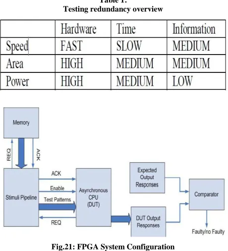
CS18: FPGA Implementation of an Asynchronous Processor with Both Online and Offline Testing Capabilities
Nikolaos Minas, Matthew Marshall, Gordon Russell and Alex Yakovlev–
[image:8.612.329.557.312.496.2]The processor uses a Concurrent Error Detection (CED) scheme to identify transient errors [18].
Table 1:
Testing redundancy overview
Fig.21: FPGA System Configuration
My inference: The implementation of an asynchronous processor on an FPGA showed a reduction in power consumption of 35%, as well as a reduction in area of 4% when compared with the synchronous equivalent. It also shows that power and area can be reduced by 40% and 9% respectively for the asynchronous CED system. FPGA based RISC processor based ATE is used to conduct both online and offline asynchronous testing to substitute conventional synchronous ATE.
CS19: On the in-field functional testing of decode units in pipelined RISC processors
Bernardi, R. Cantoro, L. Ciganda, E. Sanchez, M. Sonza Reorda, S. De Luca, R. Meregalli and A. Sansonetti –
The paper proposes a strategy to obtain high coverage figures on the decode unit of pipelined RISC processors. Result demonstrates SBST approach provides 90% coverage struck at fault while instruction based coverage approach gives 70% coverage [19].
My Inference: This author in figure has used 17 different patterns to generate various instructions to test RISC processor. Similar processor testing strategy using various test patterns is planned in my research.
Fig.22: MARCH 1 ON THE OPERANDS
II. KEY FINDINGS OF SURVEY
In general, there are two kinds of ATEs, one is dedicated and other is Universal. In Dedicated ATE, all input-output patterns are compacted, stored in a database & compared with the expected outputs [1] and Working/Not Working Condition of the Circuits can be indicated by LEDs or 7-Segment Display.
[image:8.612.54.284.316.569.2]International Journal of Emerging Technology and Advanced Engineering
Website: www.ijetae.com (ISSN 2250-2459, ISO 9001:2008 Certified Journal, Volume 7, Issue 11, November 2017)
Like Dedicated and Universal ATEs, there are two more types of ATEs namely: External and Embedded ATEs. In External ATEs, readily available ICs can be tested outside the ATE using bread board. Embedded ATEs consists of Built in Self Test along with Pattern Generator and Logic Analyzer; all these Components can be built inside the ATE and additional circuits can also be tested using this kind of ATEs.
Based on the above mentioned in-depth literature survey, almost none of the Researcher or Research work has ever attempted to design develop and implement a WIRELESS UNIVERSAL DIGITAL SOC ATE, using FGPA Design Methodology, which has several advantages, useful applications. Hence, my Research work is technically justifiable & worth all the best efforts that I have put in last 4 years.
III. CONCLUSION
All the above important authoritative work, which I have discussed in this paper as case studies are very closest to my ongoing research on Design, Simulation, Modeling and Implementation of FPGA based Digital ATE. I am very thankful to all the above researchers who have motivated and contributed immensely to my research design and research methodologies in their respective ways. I will be publishing my research experiment work with results in my upcoming papers.
REFERENCE PAPERS
[1] K Jamal and P.Srihari, “Analysis of Test Sequence Generators for Built-In Self-Test Implementation”, 2015 International Conference on Advanced Computing and Communication Systems (ICACCS -2015), Jan. 05 – 07, 2015, Coimbatore, INDIA
[2] Fumiyasu Hirose, Koichiro Takayama, and Nobuaki Kawato, “A Method to Generate Tests for Combinational Logic Circuits using an Ultrahigh-speed Logic Simulator”, 1988 International Test Conference
[3] Abdul Rafay Khatri, Ali Hayek, and Josef Borcsok, “ATPG Method with a Hybrid Compaction Technique for Combinational Digital Systems”, SAI Computing Conference 2016, London, UK
[4] Nagaraj S Vannal, Saroja V Siddamal, Shruti V Bidaralli and Mahalaxmi S Bhille, “DESIGN AND TESTING OF COMBINATIONAL LOGIC CIRCUITS USING BUILT IN SELF TEST SCHEME FOR FPGAs”, Fifth International Conference on Communication Systems and Network Technologies, 2015 [5] Ralph Nyberg, Johann Heyszl and Dietmar Heinz, “Enhancing Fault
Emulation of Transient Faults by Separating Combinational and Sequential Fault Propagation”, GLSVLSI ’16, May 18 - 20, 2016, Boston, MA, USA
[6] Zubair Ahmed, “A Method for Test Pattern Generation of Combinational Circuits Using Ordinary Algebra”, International Journal of Computer and Information Technology (2279 – 0764) Volume 01– Issue 01, September 2012
[7] Shashank Ukey, Shubhangi Rathkanthiwar and Sandeep Kakde, “VLSI Implementation of Low Power Scan Based Testing”, International Conference on Communication and Signal Processing, April 6-8, 2016, India
[8] Chih-Ang Chen and Sandeep K. Gupta, “A methodology to design efficient BIST test pattern generator”, International test conference, IEEE 1995
[9] Arun Kumar, “Design Of Low Power Test Pattern Generator For Built In Self-Test (Bist) Circuits”, International Journal of Technical Research and Applications, Volume 4, Issue 3 (May-June, 2016) [10] K. Nivitha and Anita Titus, “A BIST Circuit for Fault Detection
Using Recursive Pseudo-Exhaustive Two Pattern Generator”, International Journal of Modern Engineering Research (IJMER), Vol.2, Issue.3, May-June 2012 pp-676-681
[11] Paul P. Sotiriadis and Gregory L. Weaver, “Diophantine Frequency Synthesizer Design for Timekeeping Systems”, Hindawi Publishing Corporation International Journal of Navigation and Observation Volume 2008
[12] Long Huang, Deping Huang, and Jinghong Chen, “Implementation of Direct Frequency Synthesizer for Multiple Frequency Clock Generation”, IEEE 2014
[13] Wei-Bin Yang, Chi-Hsiung Wang, Sheng-Shih Yeh and Chao-Cheng Liao, “A multiple frequency clock generator using wide operation frequency range phase interpolator”, Microelectronics Journal 44 (2013)
[14] Wu Dan and Wei Li, “A Programmable Divider with Wide Division Range Applied in An FMCW Frequency Synthesizer”, IEEE 2015 [15] D.C. Keezer, T.H. Chen, T. Moon, D. T. Stonecypher, H.W. Choi,
S.Y. Kim and H. Yoo, “An FPGA-based ATE Extension Module for Low-Cost Multi-GHz Memory Test”, 20th IEEE European Test Symposium (ETS),2015
[16] K. L.V. Ramana Kumari, M. Asha Rani and N. Balaji, “FPGA Implementation of Memory Design and Testing”, 7th International Advance Computing Conference (IACC), IEEE 2017
[17] J.-H. Meza Escobar, S. Ostendorff and H.-D. Wuttke, “A configurable test-processor for board-level testing”, Euromicro Conference on Digital System Design, IEEE 2016
[18] Nikolaos Minas, Matthew Marshall, Gordon Russell and Alex Yakovlev, “FPGA Implementation of an Asynchronous Processor with Both Online and Offline Testing Capabilities”, 14th IEEE International Symposium on Asynchronous Circuits and Systems, IEEE 2008