International Journal of Emerging Technology and Advanced Engineering
Website: www.ijetae.com (ISSN 2250-2459,ISO 9001:2008 Certified Journal, Volume 4, Issue 8, August 2014)
471
Low-Power and Low-Area Dual Dynamic Node Hybrid
Flip-Flop Featuring Efficient Embedded Logic for Low Power
CMOS VLSI Circuits Using 120nm Technology
Meghana Pelleti
1, T. Krishna Murthy
2, K. Neelima
31PG Scholar, 2,3Assistant Professor, Dept. of ECE, Sree Vidyanikethan Engineering College, Tirupathi
Abstract—In this paper, a new dual dynamic node hybrid flip-flop (DDFF) and a novel embedded logic module (DDFF-ELM) based on DDFF are introduced. The DDFF offers power and area reduction when compared to the conventional flip-flops. The main aim of DDFF-ELM is to reduce pipeline overhead which arises due to the pipeline setup time, propagation delay and clock skew. It gives an area, power and speed efficient method to incorporate complex logic functions into the flip-flop. The performance comparisons are made in 120nm technology by using Digital Schematic and Microwind. And also here, DDFF and DDFF-ELM are compared with other flip-flop designs by implementing a 4-b Johnson Counter. Here the performance improvements indicate that proposed designs are well suited for modern high performance designs.
Keywords—Flip-flops, high-speed, low-power, embedded logic, leakage power, DDFF, pipeline overhead.
I. INTRODUCTION
Technology is moving forward from low scale integration to large scale and VLSI. The speed is also increasing from megahertz (MHz) to gigahertz (GHz). With the continuous advancing process of technology and speed of operation, the system requirements are also rising up. In deep-pipelined architectures, pushing the speed additional up demands a lower pipeline overhead. This overhead is the latency related to the pipeline elements, like the flip-flops and latches. Intensive work has been dedicated to improve the performance of the flip-flops within the past few decades . Latches and flip-flops are the basic elements for storing information. One latch or flip-flop can store one bit information. The main difference between latches and flip-flops is that for latches, their outputs are constantly affected by their inputs as long as the enable signal is asserted. In other words, when they are enabled, their content changes immediately when their inputs change. Flip-flops have their content change only either at the rising or falling edge of the enable signal. This enable signal is usually the controlling clock signal.
After the rising or falling edge of the clock, the flip-flop content remains constant even if the input changes.
Among all the types of flip-flops and latches, mostly D Flip-flop latches are used. They are often called as level-sensitive because their output follows their inputs as long as they are enabled. They are transparent during this entire time when the enable signal is asserted. There are situations when it is more useful to have the output change only at the rising or falling edge of the enable signal, which is usually the controlling clock signal.
In this paper, different types of flip-flop architectures are compared. They are Power PC 603, Hybrid Latch Flip-flop (HLFF), Semi-dynamic Flip-flop (SDFF), Conditional Data Mapping Flip-flop (CDMFF), and Cross Charge Control Flip-flop (XCFF). In general HLFF and SDFF are classic high performance flip-flops. They are having hybrid architecture, that has combined advantages of both dynamic and static structures. In addition, SDFF has a capability of incorporating logic very efficiently, because unlike the true single phase latch (TSPC), only one transistor is driven by the data input. This helps in reducing the pipeline overhead. All these flip-flops are aiming at reduction of power, delay and area. The disadvantages in the above flip-flops are reduced in DDFF and DDFF-ELM.
A recent paper introduced, in which a flip-flop architecture named Cross Charge Control Flip-flop (XCFF), which has advantages over SDFF and HLFF in terms of both power and speed. There are some disadvantages in XCFF like large hold-time requirement, redundant power dissipation, large power consumption and susceptibility to charge sharing at the internal dynamic nodes.
International Journal of Emerging Technology and Advanced Engineering
Website: www.ijetae.com (ISSN 2250-2459,ISO 9001:2008 Certified Journal, Volume 4, Issue 8, August 2014)
472
The performance of modern high performance flip-flops are compared with that of DDFF.
The remaining paper is divided as follows. Here Section II describes different types of flip-flop architectures and disadvantages of the existing flip-flop architectures and challenges in achieving high performance. In Section III, the proposed DDFF architecture and its operation, design and working principle are provided. Section IV details the proposed ELM. Finally in Section V, we conclude with the results and improvements of the proposed flip-flop designs over the existing modern high performance designs.
II. ANALYSIS OF DIFFERENT TYPES OF FLIP-FLOP
ARCHITECTURES
The flip-flop designs are basically grouped as static and dynamic design styles. The master-slave designs include, transmission gate based master-slave flip-flop and the Power PC 603 master-slave latch.
Figure.1. Power PC 603 Flip-Flop.
Here Power PC means Performance Optimization With Enhanced RISC Performance Computing. They dissipate comparatively low power and they are also having low clock-to-output (CLK-Q) delay. In synchronous systems, the latching elements have the delay overhead which is expressed by the data-to-output (D-Q) delay rather than CLK-Q delay. Here, D-Q delay is the combination of CLK-Q delay and the setup-time of the flip-flop. But the static designs lack the low D-Q delay due to their large positive setup-time, and also most of them are susceptible to flow through resulting from CLK overlap.
Power PC 603 (Figure. 1) is one of the most efficient classic static structures. The advantages of Power PC include low-power keeper structure and low latency direct path. The keeper structure in the circuit saves the leakage power. Latency is the time to complete a single instruction from start to finish. The large D-Q delay resulting from the positive setup-time is one of the disadvantages of this design. The large data and CLK node capacitances make the design inferior in performance. Despite among all these cons, static designs still remain as low power solution when the speed is not considered as a primary concern.
The dynamic flip-flops includes the modern high performance flip-flops. They are divided into purely dynamic designs and pseudo-dynamic structures. The distinctive performance improvements are achieved by having an internal precharge structure and a static output. They are called as the semi-dynamic or hybrid structures because of having a dynamic frontend and a static output. HLFF (Figure.2) and SDFF (Figure.3) fall under this category. Here the CLK overlaps to perform the latching operation.
Figure.2. Hybrid Latch Flip-Flop (HLFF).
International Journal of Emerging Technology and Advanced Engineering
Website: www.ijetae.com (ISSN 2250-2459,ISO 9001:2008 Certified Journal, Volume 4, Issue 8, August 2014)
473
Figure.3. Semi-Dynamic Flip-Flop (SDFF).
SDFF is the fastest classic hybrid structure, but it has high power consumption because of the large CLK load as well as the large precharge capacitance. Its speed is high when compared to that of the HLFF.
In conventional semi-dynamic designs, the major sources of power dissipation are the redundant data
transitions and large precharge capacitance. The
Conditional Data Mapping Flip-Flop (CDMFF) which is present in Figure. 4. is the most efficient attempt to reduce the redundant data transitions in the flip-flop.
Figure.4. Conditional Data Mapping Flip-Flop (CDMFF).
CDMFF uses an output feedback structure to conditionally feed the data to the flip-flop which reduces overall power dissipation by eliminating unwanted transitions when a redundant event is predicted. Considerable speed performance is there, since there are no added transistors at the output node, similar to that of the HLFF.
The presence of the conditional structures in the critical path increase the hold time requirement and D-Q delay of the flip-flop. The CDMFF circuit is bulky and cause an increase in power dissipation at higher data activities due to the additional transistors added for the conditional circuitry.
In a wide variety of designs, the large precharge capacitance results due both the output up and the pull-down transistors are driven by the prcharge node. Most of the capacitance at this precharge node is due to the transistors being driving large output loads. This drawback is considered in the design of XCFF (Figure. 5).
Figure.5. Cross Charge Control Flip-Flop (XCFF).
XCFF reduces the power dissipation by splitting the dynamic node into two, each one separately driving the output pull-up and pull-down transistors. The total power consumption is almost reduced without any degradation in speed because, only one of the two dynamic nodes is switched during one clock cycle. XCFF has a comparatively lower CLK driving load. The major drawback of this design is that, the redundant precharge at node X2 and X1 for data patterns containing more 0s and 1s respectively. Due to the conditional shutoff mechanism, the large hold time requirement appears, and a low to high transition in the CLK when the data is low, causes charge sharing at node X1. This charge sharing can trigger erroneous transition at the output, unless the inverter pair INV1-2 is carefully skewed. The problem of charge sharing becomes very high when complex functions are embedded into the design.
III. PROPOSED DDFFARCHITECTURE
International Journal of Emerging Technology and Advanced Engineering
Website: www.ijetae.com (ISSN 2250-2459,ISO 9001:2008 Certified Journal, Volume 4, Issue 8, August 2014)
474
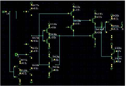
[image:4.612.48.290.175.340.2]So, called as dual dynamic. As it is having dynamic frond end and static output, it is hybrid in nature. So this is the reason for calling this flip-flop as DDFF (Figure. 6).
Figure.6. Dual Dynamic Node Hybrid Flip-Flop (DDFF).
In DDFF, node X1 is pseudo-dynamic with a weak inverter acting as a keeper. Node X2 is purely dynamic when compared to XCFF. Here we provide unconditional shutoff mechanism at the frontend where as conditional shutoff mechanism in XCFF. The DDFF operates in two phases:
1) The Evaluation Phase, when CLK is high, and 2) The Precharge Phase, when CLK is low.
The actual latching occurs in evaluation phase during 1-1 overlap of CLK and CLKB. If D is high (prior to this overlap period), node X1 is discharged from NM0-2, this switches the cross coupled inverter pair INV1-2 which causes node X1B to high and output QB discharge through NM4. For low level, node X1 retained by inverter pair INV1-2, for the rest of evaluation phase no latching occurs. Node X2 is held held high throughout evaluation period by pMOS transistor PM1. As CLK falls low, the circuit enters in the precharge phase and node X1 pulled high through PM0, switching the state of INV1-2. During this period node X2 is not actively driven by any transistor, it stores the charge dynamically. The outputs at node QB and
maintain their voltage levels through INV3-4.
If D is low i.e zero (prior to the overlap period), node X1 remains high and node X2 pulled low through NM3 as the CLK goes high. Thus, node QB is charged high through PM2 and NM4 is held off. At the end of the evaluation phase, as the CLK falls low, node X1 remains high and X2 stores the charge dynamically.
The circuit exhibits negative setup time due to the short transparency period defined by the 1-1 overlap of CLK and CLKB allows the data to be sampled even after the rising edge of the CLK before CLKB falls low. The minimum time period before the CLK edge is setup time and the minimum time period after the CLK edge is the hold time, where the data should be stable so that proper sampling is possible. Here setup time and hold time depend on the CLK overlap period.
IV. PROPOSED ELM
[image:4.612.323.564.350.527.2]As earlier we mentioned, the major advantage of the SDFF is the capability to incorporate the complex logic functions efficiently. The efficiency in terms of speed and area can be predicted from the fact that an N-input function can be realized in appositive edge triggered structure using a pull-down network (PDN) consisting of N transistors as shown in Figure. 7.
Figure.7. SDFF-ELM
This embedded structure offers a very fast and small implementation. Although SDFF is capable of offering efficiency in terms of speed and area, it is not a good solution as far as power consumption is concerned. So we consider SDFF with embedded logic for comparative purposes.
International Journal of Emerging Technology and Advanced Engineering
Website: www.ijetae.com (ISSN 2250-2459,ISO 9001:2008 Certified Journal, Volume 4, Issue 8, August 2014)
[image:5.612.50.289.136.294.2]475
Figure.8. Proposed DDFF-ELM
In the proposed model, the transistor driven by the data input is replaced by the PDN and the clocking scheme in the frontend is changed. The reason for this in clocking is the charge sharing, which becomes uncontrollable as the number of nMOS transistors in the stack increases. The same reason makes XCFF also incapable of embedding complex logic functions. As the size and number of the stacked nMOS transistor increases, the charge sharing becomes uncontrollably large.
Here by using the above flip-flops a Johnson up-down counter can be designed and the results are compared accordingly.
[image:5.612.321.566.136.229.2]Figure.9. Johnson Counter Using SDFF
[image:5.612.318.571.374.587.2]Figure.10. Johnson Counter Using XCFF
Figure.11. Johnson Counter Using DDFF
From the above Figures. 9, 10, and 11, Johnson Counter is designed with the help of SDFF, XCFF and DDFF respectively. All the results are compared with respect to counter.
V. RESULTS
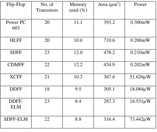
[image:5.612.47.289.455.637.2]The performance comparisons of the all flip-flops are given in the below table.
TABLE I
PERFORMANCE COMPARISON OF VARIOUS FLIP-FLOPS
Flip-Flop No. of
Transistors
Memory used (%)
Area (µm2) Power
Power PC 603
20 11.1 393.2 0.300mW
HLFF 20 10.6 710.6 0.206mW
SDFF 23 12.0 478.2 0.210mW
CDMFF 22 12.2 454.9 0.202mW
XCFF 21 10.2 367.6 51.626µW
DDFF 18 9.5 305.1 18.084µW
DDFF-ELM
23 8.4 287.3 16.531µW
SDFF-ELM 22 8.8 316.4 73.442µW
[image:5.612.49.290.456.534.2]International Journal of Emerging Technology and Advanced Engineering
Website: www.ijetae.com (ISSN 2250-2459,ISO 9001:2008 Certified Journal, Volume 4, Issue 8, August 2014)
[image:6.612.48.291.114.436.2]476
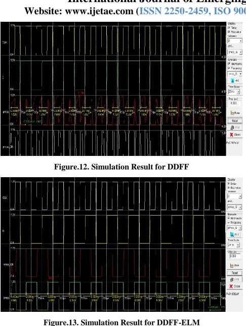
Figure.12. Simulation Result for DDFF
Figure.13. Simulation Result for DDFF-ELM
From the above results we can notice the performance improvements in DDFF and DDFF-ELM.
By using these flip-flops, as earlier mentioned Johnson Counter is designed. The performance comparisons for these counter is given below in the Table II.
Table II
Performance Comparision Of Flip-Flops With Johnson Counter
Flip-Flop No. of
Transistors
Memory
Used (%)
Area (µm2) Power
(mW)
SDFF 92 33.5 1378.3 0.542
XCFF 84 30.5 1200.9 0.114
DDFF 72 27.7 1034.5 0.104
From the above table we can notice that the power and area are reduced in DDFF when compared to the other flip-flops.
VI. CONCLUSION
In this paper, a new low power and low area DDFF and a novel DDFF-ELM were proposed. The proposed DDFF eliminates the redundant power dissipation present in XCFF. Comparison of the proposed flip-flop with the other flip-flops showed that it exhibits lower power dissipation along with area and speed performances. The efficiency of the flip-flop and the ELM were further highlighted using Johnson up-down counter. It was proven that the proposed architectures are well suited for modern high performance designs where area, delay overhead and power dissipations are of major concern.
REFERENCES
[1] Kalarikkal absel, Lijo Manuel, and R. K. Kavitha, “Low-Power Dual Dynamic Node Pulsed Hybrid Flip-Flop Featuring Efficient Embedded Logic” in IEEE VLSI Transactions (Volume:21 Issue:9) pp. 1693-1704.
[2] Ahmed Sayed and Hussain Al-Assad, 2011, „Low-Power Flip-Flops: Survey, Comparative Evaluation and a New Design, IACSIT International Journal of Engineering and Technology, Vol.3, No.3. [3] Ismail.S.M. and Islam.F.T.,2012,‟Low Power design of Johnson
Counter using clock gating‟ International Conference on Computer and Information Technology (ICCIT),pp 510-517.
[4] G. Gerosa, S. Gary, C. Dietz, P.Dac, K. Hoover, J. Alvarez, H.Sanchez, P. Ippolito, N. Tai, S. Litch, J. Eno, J. Golab, N. Vanderschaaf, and J. Kahle, “A 2.2 W, 80 MHz superscalar RISC microprocessor,” IEEE J. Solid-State Circuits, vol. 29, no. 12, pp. 1440-1452, Dec. 1994.
[5] C. K. Teh, M. Hamada, T. Fujita, H. Hara, N. Ikumi, and Y. Oowaki, “Conditional data mapping flip-flops for low-power and high-performance systems,” IEEE Trans. Very Large Scale Integr.(VLSI) Syst., vol. 14, no. 12, pp. 1379-1383, Dec, 2006.
[6] P. Zhao, T . K. Darwish, and M. A. Bayoumi, “High- Performace and low-power conditional discharge flip-flop,”IEEE Trans. Very Large Scale Integr. (VLSI) Syst., Syst., vol. 12, no .5, pp. 477-484, May 2004.
[7] S. H. Rasouli, A. Khadermzadesh, A. Afzali-Kusha, and M. Nourani, “Low-Power Single- and double-edge-triggered flip-flop for high-speed applications,” Proc. Inst. Elect. Eng. Circuits Devices Syst., vol. 152, no. 2, no. 2, pp. 118-122, Apr. 2005.
[8] A. Ma and K. Asanovic, “A double-pulsed set- conditional-reset flipflop,” Laboratory for Computer Science, Massachusetts Inst. Technology, Cambridge, Tech. Rep. MIT-LCS-TS-844, May 2002. [9] H. Mahmoodi, V. Tirumalashetty, M. Cooke, and K. Roy, “Ultra