DPV 11 serial synchronous
interface technical manual
EK-DPV11-TM-002
1st Edition, July 1980
2nd Printing (Rev), November 1980
Copyright © 1980 by Digital Equipment Corporation
All Rights Reserved
The material in this manual is for informational pur-poses and is subject to change without notice.
Digital Equipment Corporation assumes no responsi-bility for any errors which may appear in this manual.
Printed in U.S.A.
This document was set on DIGITAL's DECset-8000 computerized typesetting system.
The following are trademarks of Digital Equipment Corporation, Maynard, Massachusetts:
DIGITAL DEC PDP DECUS UNIBUS DECLAB
DECsystem-IO DECSYSTEM-20 DIBOL
EduSystem VAX VMS
MASSBUS OMNIBUS OS/8 RSTS RSX
lAS
CHAPTER 1
1.1 1.2 1.3 1.4 1.5 1.5.1 1.5.2 1.5.3 1.6 1.7
CHAPTER 2
2.1 2.2 2.3 2.4 2.4.1 2.4.2 2.5
CHAPTER 3
3.1 3.2 3.3 3.3.1 3.3.2 3.3.3 3.3.4 3.3.5 3.4 3.4.1 3.4.2 3.5
CONTENTS
Page
INTRODUCTION
SCOPE ... 1-1 DPVll GENERAL DESCRIPTION ... 1-1 DPVll OPERATION ... 1-2 DPVll FEATURES ... 1-2 GENERAL SPECIFICATIONS ... 1-2 Environmental Specifications ... 1-2 Electrical Specifications ... 1-3 Performance Parameters ... 1-3 DPVll CONFIGURATIONS ... 1-3 EIA STANDARDS OVERVIEW ... 1-3
INSTALLATION
INTRODUCTION ... 2-1 UNPACKING AND INSPECTION ... 2~1
PRE-INSTALLATION REQUIREMENTS ... 2-1 INSTALLATION ... 2-6
Verification of Hardware Operation ... 2-7 Connection to External Equipment/Link Testing ... 2-8 TEST CONNECTORS ... 2-8
REGISTER DESCRIPTIONS AND PROGRAMMING INFORMATION
CHAPTER 4 4.1 4.2 4.2.1 4.2.1.1 4.2.1.2 4.2.1.3 4.2.1.4 4.2.1.5 4.2.1.6 4.2.1.7 4.2.1.8 4.2.1.9 4.2.1.10 4.2.2 4.2.2.1 4.2.2.2 4.3 4.3.1 4.3.1.1 4.3.1.2 4.3.1.3 4.3.1.4 4.3.2 4.3.2.1 4.3.2.2 4.3.3 4.3.3.1 4.3.3.2 4.3.3.3 4.3.4 4.3.5 4.3.6 4.3.7 4.3.8 4.3.9 4.3.10 CHAPTERS 5.1 5.2 5.3 5.4 5.5 5.5.1 5.5.2 5.5.3 5.5.3.1 5.5.3.2 5.5.3.3
CONTENTS (Cont)
Page
TECHNICAL DESCRIPTION
INTRODUCTION ... 4-1 FUNCTIONAL DESCRIPTION ... 4-1 Logic Description ... 4-1 Bus Transceivers ... 4-1 Read/Write Control ... 4-1 USYNRT and Bidirectional Buffer ... 4-1 Receive Control and Status Register ... 4-1 Transmit Control and Status Register ... 4-1 Interrupt Logic ... 4-3 Data Set Change Logic ... 4-3 Clock Circuit ... 4-3 EIA Level Converters ... 4-3 Charge Pump ... 4-3 General Operational Overview ... 4-3 Receive Operation ... 4-3 Transmit Operation ... 4-5 DETAILED DESCRIPTION ... 4-5 Bus Transceivers ... 4-5 Address Selection ... 4-5 Address Decode ... 4-6 Bus Data Transfers ... 4-6 Vector Generation ... 4-6 Read/Write Control Logic ... 4-6 Register Decode ... 4-6 USYNRT Control ... 4-7 USYNRT, RXCSR and PCSCR ... 4-7 USYNRT ... 4-10 Receive Control and Status Register ... 4-10 Parameter Control and Character Length Register ... 4-10 Interrupt Logic ... 4-10 Data Set Change Circuit. ... 4-11 Clock Circuit ... 4-11 USYNRT Timing ... 4-12 EIA Receivers ... 4-12 EIA Drivers ... ... ... ... ... ... 4-12 Maintenance Mode ... ... ... ... ... .... ... .... ... ... ... 4-12
MAINTENANCE
APPENDIX A A.1 A.2 A.3 A.4 A.4.1 A.4.2 A.S APPENDIXB APPENDIXC C.l C.2 C.3 C.4 C.S C.6 C.7 C.8 C.9 APPENDIXD GLOSSARY Figure No. 1-1 2-1 2-2 2-3 2-4 3-1 3-2 3-3 3-4 3-S 3-6 4-1 4-2 4-3 4-4 4-S A-I
CONTENTS (Cont)
Page
DIAGNOSTIC SUPERVISOR SUMMARY
INTRODUCTION ... A-I VERSIONS OF THE DIAGNOSTIC SUPERVISOR ... A-I LOADING AND RUNNING A SUPERVISOR DIAGNOSTIC ... A-I SUPERVISOR COMMANDS ... A-3 Command Switches ... A-4 Control/Escape Characters Supported ... A-4 THE SETUP UTILITy... A-S
USYNRT DESCRIPTION
IC DESCRIPTIONS
GENERAL ... C-l DC003 INTERRUPT CHIP ... C-l DC004 PROTOCOL CHIP ... C-3 DCOOS BUS TRANSCEIVER CHIP... C-3 26LS32 QUAD DIFFERENTIAL LINE RECEIVER ... C-6 8640 UNIBUS RECEIVER... C-6 8881 NAND ... C-6 9636A DUAL LINE DRIVER ... C-6 9638 DUAL DIFFERENTIAL LINE DRIVER ... C-6
PROGRAMMING EXAMPLES
ILLUSTRATIONS
Title Page
DPVll System ... 1-1 DPVll Jumper Locations ... 2-4 H32S9 Turn-Around Test Connector ... 2-8 RS-423-A with H32S9 Test Connector ... 2-10 H3260 On-Board Test Connector ... 2-11 DPVll Register Configurations and Bit Assignments ... 3-3 Receive Control and Status Register (RXCSR) Format ... 3-4 Receive Data and Status Register (RDSR) Format. ... 3-8 Parameter Control Sync/Address Register (PCSAR) Format. ... 3-11 Parameter Control and Character Length Register
(PCSCR) Format ... 3-13 Transmit Data and Status Register (TDSR) Format ... 3-17 DPVll Block Diagram ... 4-2 Simplified Functional Diagram ... 4-4
Figure No.
B-1
B-2 C-l C-2 C-3 C-4
C-5 C-6 C-7 C-8
Table No.
2-1 2-2 2-3 2-4 2-5 3-1 3-2
3-3 3-4
3-5
3-6 4-1 4-2 5-1 C-l C-2 C-3
ILLUSTRATIONS (Cont)
Title Page
Terminal Connection Identification Diagram
(2112517-0-0 Variation) ... B-2 5025 Internal Register Bit Map (2112517-0-0 Variation) ... B-3 DC003 Logic Symbol ... C-l DC004 Simplified Logic Diagram ... C-4 DC005 Simplified Logic Diagram .... ... ... ... ... ... C-7 26LS32 Terminal Connection Diagram and Terminal
Indentification ... C-9 8640 Equivalent Logic Diagram ... C-l 0 8881 Pin Identification ... C-l 0 9636A Logic Diagram and Terminal Identification ... C-ll 9638 Logic Diagram and Terminal Identification ... C-12
TABLES
Title Page
Configuration Sheet ... 2-1 Vector Address Selection ... 2-5 Device Address Selection ... 2-6 Voltage Requirements ... 2-7 H3259 Test Connections ... 2-9 DPV11 Registers ... 3-1 Receive Control and Status Register (RXCSR) Bit
Assignments ... 3-5 Receive Data and Status Register (RDSR) Bit Assignments ... 3-8 Parameter Control Sync/Address Register (PCSAR)
Bit Assignments ... 3-11 Parameter Control and Character Length Register
PREFACE
This manual was written to satisfy the needs of Field Service and Educational Service Training per-sonnel.
It contains the following categories of information.
• General description including features, specifications, and configurations
• Installation
• Programming
• Technical Description
• Maintenance
The manual also contains four appendixes which include diagnostic information, integrated circuit de-scriptions, and programming examples.
1.1 SCOPE
CHAPTER 1
INTRODUCfION
This chapter contains introductory information about the DPVll. It includes a general description, and a brief overview of the DPVll operation, features, general specifications, and configurations.
1.2 DPV11 GENERAL DESCRIPTION
The DPVll is a serial synchronous line interface for connecting an LSI-II bus to a serial synchronous modem that is compatible with EIA RS-232-C interface standards and EIA RS-423-A and RS-422-A electrical standard~. EIA RS-422-A compatibility is provided for use in local communications only (timing and data leads only). The DPVll is intended for character-oriented protocols such as BISYNC, byte count-oriented protocols such as DDCMP, or bit-oriented data communication protocols such as SDLC. The DPVl1 does not provide automatic error generating and checking for BISYNC.
The DPVll consists of one double-height module and may be connected to an EIA RS-232-C modem by a BC26L-25 (RS-232-C) cable.
The DPVll is a bus request device only and must rely on the system software for service. Interrupt control logic generates requests for the transfer of data between the DPVll and the LSI-II memory by means of the LSI-II bus. (Figure 1-1 shows the DPVll system.)
CJ)
~
co I
CJ)
....J
DPV11
CPU
MEM
BC26L- 25
TELEPHONE
RS-232-C t - -L_1 N_E _ _ ., MODEM
Figure I-I DPVll System
1.3 DPVll OPERATION
The DPVll is a double-buffered program interrupt interface that provides parallel-to-serial conversion of data to be transmitted and serial-to-parallel conversinn of received data. The DPVll can operate at speeds up to 56K b/s.* It has five 16-bit registers which can be accessed in word or byte mode. These registers are assigned a block of four contiguous LSI-II bus word addresses that start on a boundary with the low-order three bits being zeros. This block of addresses is jumper-selectable and may be located anywhere between 1600008 and 1777768. Two of these registers share the same address. One is accessed during a read from the address, the other during a write to the address. For a detailed descrip-tion of each of the five registers, refer to Chapter 3. These registers are used for status and control information as well as data buffers for both the transmitter and receiver portions of the DPVll.
1.4 DPVll FEATURES Features of the DPVll include:
• Full-duplex or half-duplex operation
• Double-buffered transmitter and receiver
• EIA RS-232-C compatibility
• All EIA RS-449 Category I modem control
• Partial Category II modem control to include incoming call, test mode, remote loopback, and local loop back
• Program interrupt on transitions of modem control signals
• Operating speeds up to 56K bls (may be limited by software or CPU memory)
• Software-selectable diagnostic loopback
• Operation with bit-, byte count-, or character-oriented protocols
• Internal cyclic redundancy check (CRC) character generation and checking (not usable with BISYNC)
• Internal bit-stuff and detection with bit-oriented protocols.
• Programmable sync character, sync insertion, and sync stripping with byte count-oriented protocols.
• Recognition of secondary station address with bit-oriented protocols.
1.5 GENERAL SPECIFICATIONS
This paragraph contains environmental, electrical, and performance specifications for the DPVll.
1.5.1 Environmental Specifications
The DPVll is designed to operate in a Class C environment as specified by DEC Standard 102 (ex-tended).
Operating Temperature Relative Humidity
50 C (41 0 F) to 600 C (140 0 F)
10% to 90% with a max. wet bulb temperature of 280 C (820 F) and a min. dew point of 20 C (360 F)
1.5.2 Electrical Specifications
The DPVll requires the following voltages from the LSI-II bus for proper operation.
+ 12 V at 0.30 A max. (0.15 A typical) +5 V at 1.2 A max. (0.92 A typical)
The interface includes a charge pump to generate a negative voltage required to power the RS-423-A drivers.
The DPVll presents 1 ac load and 1 dc load to the LSI-II bus.
1.5.3 Performance Parameters
Performance parameters for the DPVll are listed as follows.
Operating Mode
Data Format
Character Size
Max. Configuration
Max. Distance
Max. Serial Data Rates
1.6 DPVll CONFIGURATIONS
Full or half-duplex
Synchronous BISYNC, DDCMP, and SDLC
Program-selectable (5-8 bits with character-oriented protocols and 1-8 bits with bit-oriented protocols)
16 DPVll modules per LSI-II bus
15 m (50 ft) for RS-232-C. 61 m (200 ft) for RS-423-AjRS-422-A (Distance is directly dependent on speed, and 200 ft is a suggested average. See RS-449 specifica-tion for details.)
56K bjs (May be less because of software and memory refresh limitations.)
There are two DPVll configurations, the DA and the DB.
DPVII-DA
Unbundled version consists of: M8020 module
Module Configuration Sheet (EK-DPVII-CG) DPVII-DB
Bundled version consists of: M8020 module
H3259 turn-around connector BC26L-25 cable
DPVll User Manual (EK-DPVII-UG) LIB kit (ZJ314-RB)
Field Maintenance Print Set (MP00919)
Turn-around connectors, cables and documentation may be purchased separately.
1.7 EIA STANDARDS OVERVIEW (RS-449JRS-232-C)
For this reason, RS-449 standard has been developed to replace RS-232-C. It maintains a degree of compatibility with RS-232-C to accommodate an upward transition to RS-449.
The most significant difference between RS-232-C and RS-449 is in the electrical characteristics of signals used between the data communication equipment (DCE) and the data terminal equipment (DTE). The RS-232-C standard uses only unbalanced circuits, while the RS-449 uses both balanced and unbalanced electrical circuits. The specifications for the types of electrical circuits supported by RS-449 are contained in EIA standards RS-422-A for balanced circuits and RS-423-A for unbalanced circuits. These new standards permit much greater transmission speed and will allow greater distance between DTE and DCE. The maximum transmission speeds supported by RS-422-A and RS-423-A circuits vary with cable length; the normal speed limits are 20K bls for RS-423-A and 2M bls for RS-422-A, both at 61 m (200 feet).
2.1 INTRODUCTION
CHAPTER 2
INSTALLATION
This chapter provides all the information necessary for a successful installation and subsequent check-out of the DPVll. Included are instructions for unpacking and inspection, pre-installation, installation and verification of operation.
2.2 UNPACKING AND INSPECfION
The DPVll is packaged in accordance with commercial packing practices. Remove all packing mate-rial and verify that the following are present.
M8020 module
H3259 turn-around connector BC26L-25 cable
DPVll User Manual (EK-DPVII-UG) LIB kit (ZJ314-RB)
Field Maintenance Print Set (MP00919)
Inspect all parts carefully for cracks, loose components or other obvious damage. Report damages or shortages to the shipper immediately, and notify the DIGITAL representative.
2.3 PRE-INSTALLATION REQUIREMENTS
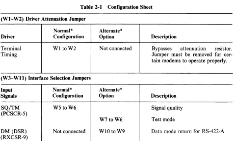
Table 2-1 (Configuration Sheet) provides a convenient, quick reference for configuring jumpers.
Table 2-1 Configuration Sheet
(WI-W2) Driver Attenuation Jumper
Normal* Alternate*
Driver Configuration Option Description
Terminal WI to W2 Not connected Bypasses attenuation resistor.
Timing Jumper must be removed for
cer-tain modems to operate properly.
(W3-Wll) Interface Selection Jumpers
Input Normal* Alternate*
Signals Configuration Option Description
SQ/TM W5 toW6 Signal quality
(PCSCR-5)
W7 toW6 Test mode
DM (DSR) Not connected WIO to W9 Data mode return for RS-422-A
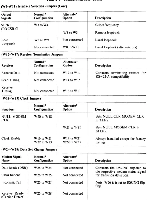
[image:13.612.83.562.459.746.2]Table 2-t Configuration Sheet (Cont)
(W3-W II) Interface Selection Jumpers (Cont)
Output Normal* Alternate *
Signals Configuration Option Description
SFjRL W3 toW4 Select frequency
(RXCSR-O)
W5 toW3 Remote loopback
Local W8 toW9 Not connected Localloopback
Loopback
Not connected W8 to Wll Localloopback (alternate pin)
(WI2-WI7) Receiver Termination Jumpers
Normal* Alternate *
Receiver Configuration Option Description
Receive Data Not connected W12 to WI3 Connects terminating resistor for RS-422-A compatibility
Send Timing Not connected W14 to W15
Receive
Timing Not connected W16 to WI7
(WIS-W23) Clock Jumpers
Normal* Alternate*
Function Configuration Option Description
NULL MODEM W20 to WI8 Sets NULL ClK MODEM CLK
CLK to 2 kHz.
W21 to WI8 Sets NULL MODEM CLK to
50 kHz.
Clock Enable WI9 to W21 WI9 to W2I Always installed except for factory
W22 to W23 W22 to W23 testing.
(W24-W2S) Data Set Change Jumpers
Modem Signal Normal* Alternate *
Name Configuration Option Description
Data Mode (DSR) W26 to W24 Not connected Connects the DSCNG flip-flop to the respective modem status signal Clear to Send W26 to W25 Not connected for transition detection.
Incoming Call W26 to W27 Not connected Note: W26 is input to DSCNG flip-flop
Receiver Ready W26 to W28 Not connected
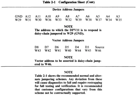
[image:14.613.54.538.77.734.2]GND AI2
W29 W31
All W30
Table 2-1 Configuration Sheet (Cont)
AIO W36
Device Address Jumpers
A9 W33
A8 W32
NOTE A7 W39
A6 W38
A5 W37
The address to which the DPVll is to respond is daisy-chain jumpered to W29 (GND).
D8 W43
D7 W42
Vector Address Jumpers
D6 W41
D5 W40
NOTE D4 W44
D3 W45
Source W46
Vector address to be asserted is daisy-chain jump-ered to W46.
NOTE
Table 2-1 shows the recommended normal and alter-nate jumpering schemes. Any deviation from these will cause diagnostics to fail and require restrapping for full testing and verification. It is recommended that customer configurations that vary from this scheme not be contractually supported.
Prior to installing the DPVII, perform the following tasks.
A4 W34
A3 W35
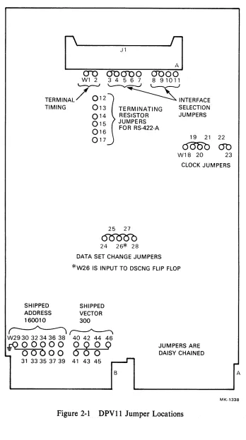
1. Verify that the following modem interface wire-wrap jumpers are installed (Figure 2-1).
W26 to W25 to W24 to W28 to W27 W22 to W23 and WI9 to W21 WI8 to W20
W5 to W6 W3 to W4 W8 to W9 WI to W2
This is the shipped configuration. Some of these jumpers may be changed when the module is connected to external equipment for a specific application. The RS-423-A NULL MODEM eLK is set to 2 kHz as shipped.
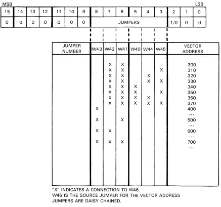
2. Based on the LSI-II bus floating vector scheme or user requirements, determine the vector address for the specific DPVII module being installed and configure W40 through W46 accordingly (Table 2-2). The floating vector ranking is 22.
[image:15.613.75.555.85.419.2]c
J 1I]
0-0 O'O<YOO 0 0 0 0/
~~~
TERMINAL 012}
~
INTERFACETIMING 013 (TERMINATING SELECTION 0 14 RESISTOR JUMPERS
O 15 JUMPERS FOR RS-422-A
016
017 19 21 22
c500b
em
W18 20 23
CLOCK JUMPERS
25 27
~
24 26* 28
DATA SET CHANGE JUMPERS
*W26 IS INPUT TO DSCNG FLIP FLOP
SHIPPED SHIPPED ADDRESS VECTOR 160010 300
~~
W2930 32 34 36 38 40 42 44 46
~OOOOO 0 0 0 0
: 00000 0 0 0
31 33 35 37 39 41 43 45
,..--..r-B
JUMPERS ARE DAISY CHAINED
I""
A
MK-1338
[image:16.612.125.473.57.680.2]Table 2-2 Vector Address Selection
DPV11 (M8020) VECTOR ADDRESSING
MSB
15 14 13 12
0 0 0 0
11 10 9 8
I
7 1 61
5 I 4 I 3 20 0 0 JUMPERS 1/0
JUMPER
NUMBER W43 W42 W41 W40 W44 W45
X X
X X X
X X X
X X X X
X X X
X X X X
X X X X
X X X X X
X
X X
X X X X X
"X" INDICATES A CONNECTION TO W46.
W46 IS THE SOURCE JUMPER FOR THE VECTOR ADDRESS JUMPERS ARE DAISY CHAINED.
LSB
1 0
0 0
VECTOR ADDRESS
300 310 320 330 340 350 360 370 400
---500
---600
---700
[image:17.612.101.538.127.536.2]
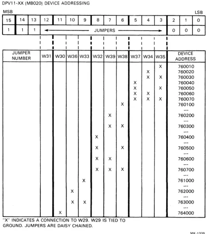
Table 2-3 Device Address Selection
DPV11-XX (M8020) DEVICE ADDRESSING
MSB
15 14 13 12111110 1 9
1
8 1 7 1 61
1 1 1...
I
JUMPER
NUMBER W31
I I
•
I W30 X I W36 X X W33 X X•
IJUMPERS
W32 W39
X
X
X
X
X X
X X
I W38 X X X X
"X" INDICATES A CONNECTION TO W29. W29 IS TIED TO GROUND. JUMPERS ARE DAISY CHAINED.
2.4 INSTALLATION
I
5
I
4I
I I
W37 W34
X X X X X X X X
3
•
W35 X X X X I I I 2 0 LSB1 0
0 0
DEVICE ADDRESS 760010 760020 760030 760040 760050 760060 760070 760100
---760200 ---760300 ---760400 ---760500 ---760600 ---760700 ---761000 ---762000 ---763000 ---764000 MK-1339The DPVII can be installed in any LSI-II bus-compatible backplane such as H9270. LSI-II con-figuring rules must be followed. Proceed with the installation as follows. For additional information refer to PDP-I 1/03 User Manual EK-LSIII-TM or LSI-II Installation Guide EK-LSI11-IG.
1. Configure the address and vector jumpers at this time if they have not been previously done (Paragraph 2.3).
2. Connect the female Berg connector on the BC26L-25 cable to J 1 on the M8020 module t and plug the module into a dual LSI-II bus slot of the backplane.
CAUTION
Insert and remove modules slowly and carefully to avoid snagging module components on the card guides.
\
3. Connect the H3259t turn-around connector to the EIA connection on the BC26L-25 cable. The jumper WI on the H3259 turn-around connector must be removed.
4. Perform resistance checks from backplane pin AA2 ( + 5 V) to ground and from AD2 (+ 12 V) to ground to ensure that there are no shorts on the M8020 module or backplane.
5. Turn system power on.
6. Check the voltages to ensure that they are within the specified tolerances (Table 2-4). If voltages are not within specified tolerances, replace the associated regulator (H780 P.S;)
Table 2-4 Voltage Requirements
Voltage Max. Min. Backplane Pin
+5V +5.25 +4.75 AA2
+I2V 12.75 + 11.25 AD2
2.4.1 Verification of Hardware Operation
The M8020 module is now ready to be tested by running the CVDPV* diagnostic. Additional informa-tion on the DPVII diagnostics is contained in Appendix A and Chapter 5. Proceed as follows.
NOTE
The
*
represents the revision level of the diagnos-tic.1. Load and run CVDPV*. Three consecutive error-free passes of this test is the minimum re-quirement for a successful run. If this cannot be achieved, check the following.
Board seating Jumper connections Cable connection Test connector
If a successful run is still unachievable, corrective maintenance is required (see Chapter 5).
2. Load and run the DEC/XII System Exerciser configured to test the number of DPVlls in the system.
Each DEC/XII CXDPV module will test up to eight consecutively addressed DPVlls.
CXDPV uses a software switch register. Refer to the nEC/Xii Cross-Reference (AS-F055C-MC) for switch register utilization.
The DEC/XII System Exerciser is designed to achieve maximum contention with all de-vices that make up the system configuration. It is within this environment that the CXDPV module runs. Its intent is to isolate DPVlls which adversely affect the system operation.
For information on configuring and running the DEC/XII System Exerciser, refer to
DEC/XII User Manual (AS-F0503B-MC) and DEC-XII Cross Reference (AS-F055C-MC).
2.4.2 Connection to External Equipment/Link Testing
The DPVll is now ready for connection to external equipment.
If the DPVll is being connected to a synchronous modem, remove the H3259 connector and install the EIA connection of the BC26L-25 cable into the connector on the modem.
Configure jumpers Wl-W28 in accordance with operating requirements (Table 2-1).
Load and run DCLT (CVCLH*) if a full link is available. This will check the final configuration and isolate failures to the CPU, the communications link, or the modem.
If the connection to external equipment uses RS-422-A, the user must provide the cable and test sup-port.
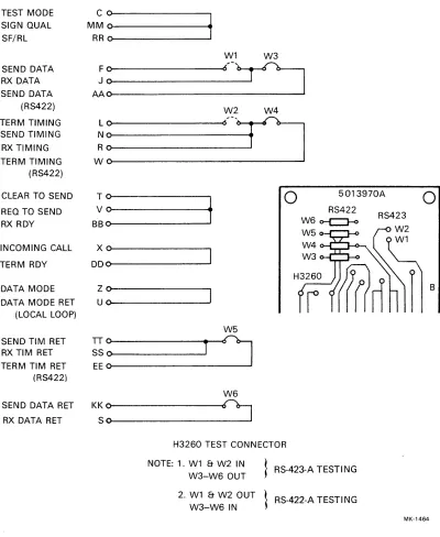
2.5 TEST CONNECTORS
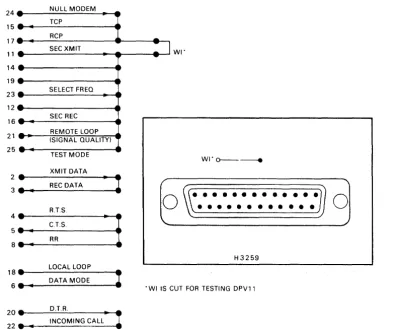
The only test connector provided with the DPVll is the H3259 turn-around connector (Figure 2-2). Table 2-5 and Figure 2-3 show the relationship between pin numbers, signal names and register bits when the H3259 is connected by means of the BC26L-26 cable to the M8020 module.
24 NULL MODEM
15 TCP
RCP 17
SEC XMIT WI·
11 14 19
23 SELECT FREQ 12
SEC REC 16
21 REMOTE LOOP (SIGNAL QUALITY) 25
TEST MODE WI" 0 - - - _____
XMIT DATA
~:
.
REC DATA"
1
0
•
•
•
•
• •
• •
•
•
• •
•
0
RTS
••••••••••••
::
:
C.T.S"
!
RRH3259
1 : :
LOCAL LOOP
DATA MODE
I
•
• WI IS CUT FOR TESTING DPV1120 •• _____ D._T._R. ____ ~,, _ _ •
22.
II INCOMING CALL •MI(.1329
[image:20.617.110.507.381.711.2]Table 2-5 H3259 Test Connections
From To
Pin No. Pin No. Pin No. Pin No.
Signal Name 83259 Jl Jl 83259 Signal Name
SEND DATA 2 F J 3 RECEIVE DATA
REQUEST TO SEND 4 V BB&T 5&8 CLEAR TO SEND
(RTS) (RXCSR-2) (CTS)(RXCSR-13),
RECEIVER READY (RR) (RXCSR-12)
LOCAL LOOPBACK 18 U Z 6 DATA MODE
(ltL) (RXCSR-3) (DM) (RXCSR-9)
SELECT FREQ/REMOTE 23/21 RR/MM MM/C 21/25 SIGNAL QUALITY /
LOOPBACK TEST MODE
(SF /RL) (RXCSR-O) (SQ/TM) (PCSCR-5)
NULL MODEM 24 L N&R 15&17 RCVCLOCK
TXCLOCK
DATA TERMINAL 20 DD X 22 INCOMING CALL
READY (DTR) (lC) (RXCSR-14)
(RXCSR-l)
The following accessories are available for interfacing and may be ordered separately.
• BC26L-X cable. Available in lengths of .3, 1.8, 2.4, 3.0, 3.6, 6.1, and 7.6 meters (1, 6, 8, 10, 12, 20 and 25 feet). When ordering, the dash number indicates the desired cable length in feet; e.g., BC26L-25 or BC26L-1.
• H3259 cable turn-around connector
• H856 Berg connector. Includes H856 Berg connector and 40 pins. Crimping tools are avail-able from:
Berg Electronics, Inc.
New Cumberland, PA 17070
• H3260 on-board test connector (includes RS-422-A testing)
The H3260 on-board test connector (Figure 2-4) may be used to test the M8020 circuitry in its entirety. RS-422-A circuitry is not tested with the H3259 cable turn-around connector. The H3260 on-board test connector is shipped configured for testing RS-422-A. It may be configured to test 422-A or RS-423-A as follows.
RS-422-A
W1-W2 out W3-W6 installed
RS-423-A
W1-W2 installed W3-W60ut The connectot is installed into J1 with the jumper side up.
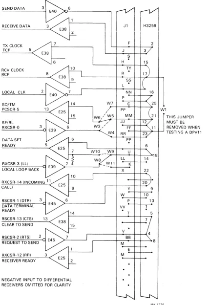
SEND DATA 3 6
RECEIVE DATA
TX CLOCK 7
TCP 5
6
RCV CLOCK RCP
LOCAL CLK 2
SQ/TM PCSCR-5
SF/RL
RXCSR-O 3
DATA SET READY
RXCSR-3 (LL) LOCAL LOOP BACK
RXCSR-14 (INCOMING 11 CALL)
RSCSR-l (DTR) 3 DATA TERMINAL READY
RSCSR-13 (CTS) CLEAR TO SEND
RSCSR-2 (RTS) 2 REQUEST TO SEND
RXCSR-12 (RR) RECEIVER READY
NEGATIVE INPUT TO DIFFERENTIAL RECEIVERS OMITTED FOR CLARITY
W7
/
W3//
W4
W10
J1
~
F 2
J 3
S
•
H 15
TY R
·
SS
•
L
NN 16
P
C 25
PP MM
JJ 12
FF
RR 23
PP
• 6
U
18
LL 14
K
X 22
20
Y 9
W 10
P 13
VV
.
T 5
V SB
M 8
E M
Figure 2-3 RS-423-A with H3259 Test Connector
W1
[image:22.613.87.515.69.693.2]TEST MODE SIGN QUAL SF/RL
SEND DATA RX DATA SEND DATA
(RS422)
TERM TIMING SEND TIMING
RX TIMING TERM TIMING
(RS422)
CLEAR TO SEND
REQ TO SEND RX RDY
INCOMING CALL
TERM RDY
DATA MODE DATA MODE RET
(LOCAL LOOP)
SEND TIM RET RX TIM RET TERM TIM RET
(RS422)
SEND DATA RET RX DATA RET
~~~
i
W1 W3 Fa
~~
____
r?=:J
W2 W4 La
;:
~'--rJ
B~:
t
o
5013970A
o
D~:
~:
E~
K~:
W6
r:J
RS422 W60-C:J-0
H3260 TEST CONNECTOR
NOTE: 1. W1 & W2 IN W3-W6 OUT
2. W1 & W2 OUT W3-W6 IN
RS-423-A TESTING
RS-422-A TESTI NG
Figure 2-4 H3260 On-Board Test Connector
RS423
B
[image:23.612.113.513.75.563.2]CHAPTER 3
REGISTER DESCRIPTIONS
AND PROGRAMMING INFORMATION
3.1 INTRODUCTION
This chapter describes the bit assignments and programming considerations for the DPV11. Some typ-ical start and receive sequences for both bit- and character-oriented protocols are included.
3.2 DPVll REGISTERS AND DEVICE ADDRESSES
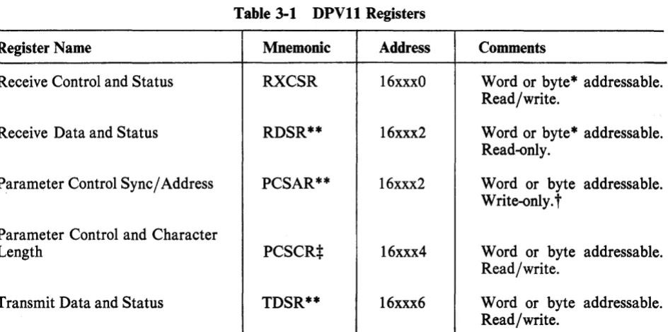
The five registers used in the DPV11 are shown in Table 3-1. Note that two of the registers (PCSAR and RDSR) have the same address. This does not constitute a conflict, however, because the PCSAR is a write-only register and the RDSR is a read-only register. These five registers occupy eight con-tiguous byte addresses which begin on a boundary where the low-order three bits are zero, and can be located anywhere between 1600008 and 1777768.
Table 3-1 DPVll Registers
Register Name Mnemonic Address Comments
Receive Control and Status RXCSR 16xxxO Word or byte* addressable.
Read/write.
Receive Data and Status RDSR** 16xxx2 Word or byte* addressable.
Read-only.
Parameter Control Sync/Address PCSAR** 16xxx2 Word or byte addressable. Write-only.
t
Parameter Control and Character
Length PCSCR:I: 16xxx4 Word or byte addressable.
Read/write.
Transmit Data and Status TDSR** 16xxx6 Word or byte addressable.
Read/write.
*
Reading either byte of these registers, clears data and certain status bits in other bytes. See Paragraphs 3.3.1 and 3.3.2.**
Registers contained within the USYNRT.t
It is not possible to do bit set or bit clear instructions on this register.*
The high byte of this register is internal to the USYNRT. [image:24.613.91.563.347.581.2]Most of the DPVll registers are internal to the USYNRT. Only the receiver control and status regis-ter (RXCSR) and the low byte of the parameregis-ter control and characregis-ter length regisregis-ter (PCSCR) are external.
NOTE
When using the special space sequence function, all registers internal to the USYNRT must be written in byte mode.
3.3 REGISTER BIT ASSIGNMENTS
Bit assignments for the five DPVl1 registers are shown in Figure 3-1. Paragraphs 3.3.1-3.3.5 provide a description of each register using a bit assignment illustration and an accompanying table with a de-tailed description of each bit.
3.3.1 Receive Control and Status Register (RXCSR) (Address 16xxxO)
Figure 3-2 shows the format for the receive control and status register (RXCSR). Table 3-2 is a de-tailed description of the register. This register is external to the USYNRT.
NOTE
The RXCSR can be read in either word or byte mode. However, reading either byte resets certain status bits in both bytes.
3.3.2 Receive Data and Status Register (RDSR) (Address 16xxx2)
Figure 3-3 show the format for the receive data and status register (RDSR). It is a read-only register and shares its address with the parameter control sync/address register (PCSAR) which is write-only. Table 3-3 is a detailed description of the RDSR.
NOTE
The RDSR can be read in either word or byte mode. However, reading eitber byte resets data and certain status bits in both bytes of this register as well as bits 7 and 10 of the RXCSR.
3.3.3 Parameter Control Sync/Address Register (PCSAR) (Address 16xxx2)
The parameter control sync/address register (PCSAR) is a write-only register which can be written in either byte or word mode. Figure 3-4 shows the format and Table 3-4 is a detailed description of the PCSAR. This register shares its address with the RDSR.
NOTE
Bit set (BIS) and bit clear (BIC) instructions can-not be executed on the PCSCR, since they execute using a read-modify-write sequence.
3.3.4 Parameter Control and Character Length Register (PCSCR) (Address 16xxx4)
The parameter control and character length register (PCSCR) can be read from or written into in either word or byte mode. The low byte of this register is external to the USYNRT and the high byte is internal. Figure 3-5 shows the format and Table 3-5 is a detailed description of the PCSCR.
3.3.5 Transmit Data and Status Register (TDSR) (Address 16xxx6)
The format for the transmit data and status register (TDSR) is shown in Figure 3-6 and Table 3-6 is a detailed description. The TDSR is a read/write register which can be accessed in either word or byte mode with no restrictions. All bits can be read from or written into and are reset by Device Reset or Bus INIT except where noted.
RXCSR 16XXXO READ/WRITE
15 14
R R
I
DATA SET 13 RI
CLR TO CHANGE SENDINCOMING CALL
RDSR 16XXX2 READ ONLY
15 14 13 12 R RCVR READY 12 ASSEMB~ED
BIT COUNT
I I
I
ERROR CHECK
PCSAR 16XXX2 WRITE ONLY
15 14 13 12
I
I
ALL STRIP PARTIES SYNC OR
ADDR LOOP MODE PROTOCOL SECD
SELECT ADRS MODE SEL 11 R
I
RCV ACTIVE 1 1I
RCVR OVER RUN 11I
IDLE MODE SELECT10 09 08 07 06 05 04 03 02 01
R R R R R/W RIW R/W RIW R/W RIW
I
I
I
I
I
DATA RCV DATA LOCAL DATA MODE DATA SET (LL) TERM READY INTR LOOP RDY
EN
RCVR SYNC RCV RX REQ STATUS OR INTR ENA TO
READY FLAG EN SEND
DETECT
10 09 08 07
I I I I J I
RECEIVE DATA BUFFER
I I I I I I
I
END OF MESG RCV START ABORT OF
MESG
10 09 08 07
ERROR DETECTION
I I I I I I
SELECTION SECONDARY STATION
+
RECEIVER SYNCI
,
~ I I I I IFigure 3-1 DPV11 Register Configurations and Bit Assignments (Sheet 1 of 2)
[image:26.615.86.572.97.632.2]
''<c'''''-pestR
16XXX4
REAOIWRITE
1 5 1 4
I I
RIW R/W
I I
,
v 1 3
R/W
TRANSMITTER CHARACTER LENGTH
TOSR
16XXX6
REAOIWRITE
15 14 13 I
R 0 0
, ,
I
I
\.Y 1 2 R/W I
I
EXTD ADDR FIELD 12 I 0 IXMIT RESERVED DATA LATE 1 1 R/W EXTD CONT FIELD 11 R/W I
I
XMIT GO AHEAD1 0 09 08 I I
R/W R/W R/W I I
\. y
RECEIVER CHARACTER LENGTH
10 09 R/W R/W
I
END OF MESG ABORT 08 RIW START OF MESG07 06
R R/W
I
I
RSVD XMIT INTR EN 07 TR/W R/W
I
\.
05 04 03 02 01 R/W R/W RIW R R
I
I
I
SQ/TM MAINT XMTR
MODE ACTIVE SELECT
XMTR XMTR
ENAB BUFFER EMPTY
T I I I I R/W R/W RIW RIW R/W
I 1 I I 1
v
TRANSMIT DATA BUFFER
Figure 3-1 DPVll Register Configurations and Bit Assignments (Sheet 2 of 2)
7 RDAT RY** 15 OS' CNG 6 RX ITEN 14
5 4
DS RX ITEN ENA
13 12 3 LL 11 RX ACT 2 RTS 10 o
TR SF/RL
9 8
OM SFD
* THIS BIT IS RESET BY READING EITHER BYTE OF THIS REGISTER. * * THESE BITS ARE RESET BY READING EITHER BYTE OF RSDR,
[image:27.615.46.521.78.448.2]MK·1327
Figure 3-2 Receive Control and Status Register (RXCSR) Format
Bit
15
14
13
12
11
Table 3-2 Receive Control and Status Register (RXCSR) Bit Assignments
Name
Data Set Change (DSCNG)
Incoming Call (IC)
Clear to Send (CTS)
Receiver Ready (RR)
Receiver Active (RXACT)
Description
This bit is set when a transition occurs on any of the following modem control lines:
Clear to Send (. "1'" ~
Data Mode ~
Receiver Ready
t,JJ
Incoming CallR1
Transition detectors for each of these four lines can be disabled by removing the associated jumper.
Data Set Change is cleared by reading either byte of the RXCSR or by Device Reset or Bus INIT.
Data Set Change causes a receive interrupt if DSITEN (bit 5) and RXITEN (bit 6) are both set.
This bit reflects the state of the modem Incoming Call line. Any transition of this bit causes Data Set Change bit (bit 15) to be asserted unless the Incoming Call line is disabled by removing its jumper. This bit is read-only and cannot be Gleared by soft-ware.
This bit reflects the state I: of the Clear to Send line of the modem. Any transition of this line causes Data Set Change (bit 15) to be set unless the jumper enabling the Clear to Send signal is removed.
Clear to Send is a program read-only bit and cannot be cleared
by software. .
This bit is a direct reflection of modem Receiver Ready lead. It indicates that the modem is receiving a carrier signal. For exter-nal maintenance loopback, this sigexter-nal must be high. If the line is open, RR is pulled high by the circuitry.
Any transition of this bit ,causes Data Set Change (bit 15) to be asserted unless the jumper enabling the Receiver Ready signal is removed.
Receiver Ready is a read-only bit and cannot be cleared by soft-ware.
This bit is set when the USYN~.T presents the first character of a message to the DPVll. It remains set until the receive data path of the USYNRT becomes idle.
Bit
10
9
8
7
I
Table 3-2 Receive Control and Status Register (RXCSR) Bit Assignments (Cont)
Name
Receiver Status Ready (RSTARY)
Data Mode (DM) (Data Set Ready)
Sync or Flag Detect (SFD)
Receive Data Ready (RDATRY)
Description
Receiver Active is a read-only bit which reflects the state of the USYNRT output pin 5.
This bit indicates the availability of status information in the upper byte of the receive data and status register (RDSR). It is set when any of the following bits of the RDSR are set: Receiver End of Message (REOM); Receiver Overrun (RCV OVRUN); Receiver Abort or Go Ahead (RABORT); Error Check (ERRCHK) if VRC is selected.
Receiver Status is cleared by any of the following conditions: reading either byte of the RDSR; clearing Receiver Enable (bit 4 of RXCSR); Device Reset, or Bus Init.
When set, Receiver Status Ready causes a receive interrupt if Receive Interrupt Enable (bit 6) is also set.
Receiver Status Ready is a read-only bit which reflects the state of USYNRT pin 7.
This bit reflects the state of the Data Mode signal from the modem.
When this bit is set it indicates that the modem is powered on and not in test, talk or dial mode.
Any transition of this bit causes the Data Set Change bit (bit 15) to be asserted unless the Data Mode jumper has been re-moved.
Data Mode is a read-only bit and cannot be cleared by software.
This bit is set for one clock time when a flag character is tected with bit-oriented protocols, or a sync character is de-tected with character-oriented protocols.
SFD is a read-only bit which reflects the state of USYNRT pin 4.
This bit indicates that the USYNRT has assembled a data char-acter and is ready to present it to the processor.
If this bit becomes set while Receiver Interrupt Enable (bit 6) is set, a receive interrupt request will result.
Receive Data Ready is reset when either byte of RDSR is read, Receiver Enable (bit 4) is cleared, or Device Reset or Bus INIT is issued.
RDATRY is a read-only bit which reflectes the state of US-YNRT pin 6.
Bit
6
5
4
3
2
1
Table 3-2 Receive Control and Status Register (RXCSR) Bit Assignments (Cont)
Name
Receiver Interrupt Enable (RXITEN)
Data Set Interrupt Enable (DSITEN)
Receiver Enable (RXENA)
Local Loop back (LL)
Request to Send (RTS)
Terminal Ready (TR) (Data Terminal Ready)
Description
When set, this bit allows interrupt requests to be made to the receiver vector whenever RDATRY (bit 7) becomes set.
The conditions which cause the interrupt request are the asser-tion of Receive Data Ready (bit 7), Receive Status Ready (bit
10), or Data ;Set Change (bit 15) if DSITEN (bit 5) is also set.
RXITEN is a program read/write bit and is cleared by Device Reset or Bus INIT.
This bit, when set along with RXITEN, allows interrupt requests to be made to the receiver vector whenever Data Set Change (bit 15) becomes set.
DSITEN is a program read/write bit and is cleared by Device Reset or Bus INIT.
This bit controls the operation of the receive section of the US-YNRT.
When this bit is set, the receive section of the USYNRT is en-abled. When it is reset the receive section is disen-abled.
In addition to disabling the receive section of the USYNRT, re-setting bit 4 reinitializes all but two of the USYNRT receive registers. The two registers not reinitialized are the character length selection buffer and the parameter control register.
Asserting this bit causes the modem connected to the DPVll to establish a data loopback test condition.
Clearing this bit restores normal modem operation.
Local Loopback is program read/write and is cleared by Device Reset or Bus request to Send is program read/write and is -Cleared -by Device~Reset'-or Bus INIT.
Setting this bit asserts the Request to Send signal at the modem interface.
Request to Send is program read/write and is cleared by Device Reset or Bus INIT.
When set, this bit asserts the Terminal Ready signal to the modem interface.
Bit
o
Bit
15
Table 3-2 Receive Control and Status Register (RXCSR) Bit Assignments (Cont)
Name
Select Frequency or Remote
Loopback (SF jRL)
7
15
ERR CHK
6
14
Description
This bit can be wire-wrap jumpered to function as either select frequency or remote loopback. When jumpered as select fre-quency (W3 to W4), setting this bit selects the modem's higher frequency band for transmission to the line and the lower fre-quency band for reception from the line. The clear condition se-lects the lower frequency for transmission and the higher fre-quency for reception.
When jumpered for remote loopback (W5 to W3), this bit, when asserted, causes the modem connected to the DPVll to signal when a remote loopback test condition has been established in the remote modem.
SF /RL is program read/write and is cleared by Device Reset or Bus INIT.
5 4 3 2
o
;
:
13 12 11 10 9 8
ASSEMB~ED IREC
BIT COUNT !OVRUN ABORT REOM RSOM I I
MK-1326
Figure 3-3 Receive Data and Status Register (RDSR) Format
Table 3-3 Receive Data and Status R~gister (RDSR) Bit Assignments
Name
Error Check (ERR CHK)
Description
This bit when set, indicates a possible error. It is used in con-junction with the error detection selection bits of the parameter control sync/address register (bits 8-10) to indicate either an error or an all zeros state of the CRC register.
With bit-oriented protocols, ERR CHK indicates that a CRC error has occurred. It is set when the Receive End of Message bit (RDSR bit 9) is set.
[image:31.620.55.534.61.525.2]Bit
14-12
11
Table 3-3 Receive Data and Status Register (RDSR) Bit Assignments (Cont)
Name
Assembled Bit Count (ABC)
Receiver Overrun (RCV OVRUN)
Description
message or not. If VRC parity is selected, this bit is set for every character which has a parity error.
ERR CHK is cleared by reading the RDSR, clearing RXENA (RXCSR bit 4), Device Reset or Bus INIT.
Used only with bit-oriented protocols, these bits represent the number of valid bits in the last character of a message. They are all zeros unless the message ends on an unstated boundary. The bits are encoded to represent valid bits as shown below.
14 13 12 Number of Valid Bits
0 0 0 All bits are valid 0 0 1 One valid bit 0 1 0 Two valid bits 0 1 1 Three valid bits
1 0 0 Four valid bits
1 0 1 Five valid bits
1 1 0 Six valid bits
1 1 1 Seven valid bits
These bits are presented simultaneously with the last bits of data and are cleared by reading the RDSR or by resetting RXENA (bit 4 of RXCSR).
This bit is used to indicate that an overrun situation has oc-curred. Overrun exists when the data buffer (bits 0-7 of RDSR) has not been serviced within one character time.
As a general rule, the overrun is indicated when the last bit of the current character has been received into the shift register of the USYNRT and the data buffer is not yet available for a new character.
Two factors exist which modify this general rule and apply only to bit-oriented protocols.
The first factor is the number of bits inserted into the data stream for transparency. For each bit inserted during the for-matting of the current character, the controller's maximum re-sponse time is increased by one clock cycle.
Bit
10
9
8
7-0
Table 3-3 Receive Data and Status Register (RDSR) Bit Assignments (Cont)
Name
Receiver Abort or Go Ahead (RABORT)
Receiver End of Message (REOM)
Receiver Start of Message (RSOM)
Receive Data Buffer
Description
This bit is used only with bit-oriented protocols and indicates that either an abort character or a go-ahead character has been received. This is determined by the Loop Mode bit (PCSAR bit 13). If the Loop Mode bit is clear, RABORT indicates reception of an abort character. If the Loop Mode bit is set, RABORT indicates a go-ahead character has been received.
The setting of RABORT causes Receiver Status Ready (bit 10 of RXCSR) to be set.
RABORT is reset when the RDSR is read or when Receiver En-able (bit 4 of RXCSR) is reset.
The abort character is defined to be seven or more contiguous one bits appearing in the data stream. Reception of this bit pat-tern when Loop Mode is clear causes the receive section of the USYNRT to stop receiving and set RSTARY (bit 10 of RXCSR). The abort character indicates abnormal termination of the current message.
The go-ahead character is defined as a zero bit followed by sev-en consecutive one bits. This character is recognized as a normal terminating control character when the Loop Mode bit is set. If
Loop Mode is cleared this character is interpreted as an abort character.
This bit is used only with bit-oriented protocols and is asserted if Receiver Active (bit 11 of RXCSR) is set and a message is ter-minated either normally or abnormally. When REOM becomes set, it sets RSTARY (bit 10 of RXCSR).
REOM is cleared when RDSR is read or when Receive Enable (bit 4 of RXCSR) is reset.
Used only with bit-oriented protocols. This bit is presented to the processor along with the first data character of a message and is synchronized to the last received flag character. Setting of RSOM does not set RSTARY (RXCSR bit 10).
RSOM is cleared by Device Reset, Bus IN IT, resetting ceiver Enable (RXCSR bit 4), or the next transfer into the Re-ceive Data buffer (low byte of RDSR).
The low byte of the RDSR is the Receive Data buffer. The se-rial data input to the USYNRT is assembled and transferred to the low byte of the RDSR for presentation to the processor. When the RDSR receives data, Receive Data Ready (bit 7 of RXCSR) becomes set to indicate that the RDSR has data to be picked up. If this data is not read within one character time, a data overrun occurs.
Bit 15
14
13
7 6 5 4 3 2 o
15 14 13 12 11 10 9 8
PROT STRIP SEC I I
APA
SEL SYNC ADR IDLE ERR DET SEL
MDE 1 I
MK-1330
Figure 3-4 Parameter Control Sync/Address Register (PCSAR) Format
Table 3-4 Parameter Control Sync/Address Register (PCSAR) Bit Assignments Name
All Parties Addressed (AP A)
Protocol Select (PROT SEL)
Strip Sync or Loop Mode (STRIP SYNC)
Description
This bit is set when automatic recognition of the All Parties Ad-dressed character is desired. The All Parties AdAd-dressed charac-ter is eight bits of ones with necessary bit stuffing so as not to be confused with the abort character.
Recognition of this character is done in the same way as the sec-ondary station address (see bit 12 of this register) except that the broadcast address is essentially hardwired within the receive data path. The logic inspects the address character of each frame for the broadcast address. When the broadcast address is recognized, the USYNRT makes it available and sets Receiver Start of Message (bit 8 of RDSR).
If the broadcast address is not recognized, one of two possible actions occurs.
1. If the Secondary Address Select mode bit (bit 12) is set, a test of the secondary station address is made.
2. If bit 12 is not set or the secondary station address is not recognized, the receive section of the USYNRT renews its search for synchronizing control characters.
This bit is used to select between character- and byte count-ori-ented or bit-oricount-ori-ented protocols. It is set for character- and byte count-oriented protocols and reset for bit-oriented protocols. This bit serves the following two functions.
Bit
12
11
10--8
Table 3-4 Parameter Control Sync/Address Register (PCSAR) Bit Assignments (Cont)
Name
Secondary Address Mode (SEC ADR MDE)
Idle Mode Select (IDLE)
Error Detection Selection
(ERR DEL SEL)
Description
2. Loop Mode (bit-oriented protocols) - With bit-oriented pro-tocols, this bit is used to control the method of termination. If it is set, either a flag or go-ahead character can cause a normal termination of a message. If it is cleared, only a flag character can cause a normal termination.
This bit is used with bit-oriented protocols when automatic rec-ognition of the secondary station address is desired. If it is set, the station address of the incoming message is compared with the address stored in the low byte of this register. Only messages prefixed with the correct secondary address are presented to the processor. If the addresses do not compare, the receive section of the USYNRT goes back to searching for flag or go-ahead characters.
When SEC ADR MDE is cleared, the receive section of the USYNRT recognizes all incoming messages.
This bit is used with both bit- and character-oriented protocols.
With bit-oriented protocols, IDLE is used to select the type of control character issued when either Transmit Abort (bit 10 of TDSR) is set or a data underrun error occurs. If IDLE is set, flag characters are issued. If IDLE is clear, abort characters are issued.
With character-oriented protocols, IDLE is used to control the method in which initial sync characters are transmitted and the action of the transmit section of the USYNRT when an under-run error occurs. IDLE is cleared to cause sync characters from the low byte of PCSAR to be transmitted. When IDLE is set, the transmit data output is held asserted during an underrun er-ror and at the end of a message.
These bits are used to determine the type of error detection used on received and transmitted messages. In bit-oriented protocols, the selection is independent of character length. In character-and byte count-oriented protocols, CRC error detection is us-able only with 8-bit character lengths. The maximum character length for VRC is seven. The bits are encoded as follows.
10 9 8
0 0 0
o
0 13-12
CRC Polynomial
x16+x12+x5+ 1 (CRC CCITT) (Both CRC data registers in the transmit and receive sec-tions are set to all ones prior to the com-putation.)
Table 3-4 Parameter Control Sync/Address Register (PCSAR) Bit Assignments (Cont)
Bit Name Description
0 1 0 Not used
0 1 1 x16+x15+x2+ 1 (CRC 16) (Both CRC regis-ters set to all zeros.)
1 0 0 Odd VRC Parity (A parity bit is attached to each transmitted character.) Should be used only in character-oriented protocols.
1 0 1 Even VRC parity (Resembles odd VRC ex-cept that an even number of bits are gener-ated.)
1 1 0 Not used.
1 1 1 All error detection is inhibited.
7-0
Sync Character The low byte of PCSAR is used as either the sync character for or Secondary character-oriented protocols or as the secondary station address Address for bit-oriented protocols.The bits are right-justified with the least significant bit being bit
O.
EXTERNAL TO THE USYNRT
__
---~A---____ _
( 7 6 5 4 3 2 0 \
TX
MM TB
RSVD INT SQ/TM TXENA TXACT RESET
EN SEL EMTY
INTERNAL TO THE USYNRT
__
---A~---__
( 15 14 13 12 11 10 9 8 "
TRANSMITTER' RECEIVER I
CHARACTER LENGTH EXADD EXCON CHAR~CTER LfNGTH
I I
MK-1325
Bit
15-13
12
11
r
Table 3-5 Parameter Control and Character Length Register (PCSCR) Bit Assignments
Name
Transmitter Character Length
Extended Address Field (EXADD)
Extended Control Field (EXCON)
Description
These bits can be read or written and are used to determine the length of the characters to be transmitted.
They are encoded to set up character lengths as follows.
15 14 13
0 0 0
1 1 1
1 1 0
1 0 1
1 0 0
o
1 1o
1 00 0 1
Character Length
Eight bits per character
Seven bits per character
Six bits per character
Five bits per character (bit-oriented protocol only)
Four bits per character (bit-oriented protocol only)
Three bits per character (bit-oriented protocol only)
Two bits per character (bit-oriented protocol only)
One bit per character (bit-oriented protocol only)
These bits can be changed while the transmitter is active, in which case the new character length is assumed at the com-pletion of the current character. This field is set to a character length of eight by Device Reset or Bus INIT. When VRC error detection is selected, the default character length is eight bits plus parity.
This bit is used with bit-oriented protocols and affects the ad-dress portion of a message in receiver operations. When it is set, each address byte is tested for a one in the least significant bit position. If the least significant bit is zero, the next character is an extension of the address field. If the least significant bit is one, the current character terminates the address field and the next character is a control character.
EXADD is not used with Secondary Address Mode (bit 12 of PCSAR).
EXADD is read/write and is reset by Device Reset or Bus INIT.
EX-Table 3-5 Parameter Control and Character Length Register (PCSCR) Bit Assignments (Cont)
Bit Name
10-8 Receiver
Character Length
7 Reserved
6 Transmit Interrupt
Enable (TXINTEN)
5 Signal Quality or
Test Mode (SQ/TM)
Description
CON is set it extends the control field from one 8-bit byte to two 8-bit bytes.
EXCON is not used with Secondary Address Mode (bit 12 of PCSAR)
EXCON is read/write and is reset by Device Reset or Bus INIT.
These bits are used to determine the length of the characters to be received.
They are encoded to set up character lengths as follows.
10 9 8 Character Length
0 0 0 Eight bits per character
1 1 1 Seven bits per character
1 1 0 Six bits per character
1 0 1 Five bits per character
1 0 0 Four bits per character (bit-oriented protocols only)
0 1 1 Three bits per character (bit-oriented proto-cols only)
0 1 0 Two bits per character (bit-oriented protocols only)
0 0 1 One bit per character (bit-oriented protocols only)
Not used by the DPVll
When set, this bit allows a transmitter interrupt request to be made to the transmitter vector when Transmit Buffer Empty (TBEMTY) is asserted. Transmit Interrupt Enable (TXIN-. TEN) is read/write and is cleared by Device Reset or Bus
INIT.
This bit can be wire-wrap jumpered to function as either Signal Quality or Test Mode.
Table 3-5 Parameter Control and Character Length Register (PCSCR) Bit Assignments (Cont)
Bit
4
3
2
Name
Transmitter Enable (TXENA)
Maintenance Mode Select (MM SEL)
Transmitter Buffer Empty (TBEMTY)
Description
Whenjumpered for the test mode (W6 to W7), this bit indicates that the modem has been placed in a test condition when as-serted. The modem test condition could be established by assert-ing Local Loopback (bit 3 of RXCSR), Remote Loopback (bit 0 of RXCSR) or other means external to the DPVll.
When SQ/TM is clear, it indicates that the modem is not in test mode and is available for normal operation.
SQ/TM is program read-only and cannot be cleared by soft-ware.
This bit must be set to initiate the transmission of data or con-trol information. When this bit is cleared, the transmitter will revert back to the mark state once all indicated sequences have been completed. TXENA should be cleared after the last data character has been loaded into the transmit data and status reg-ister (TDSR). Transmit End of Message (bit 9 of TDSR) should be asserted when TXENA is reset (if it is to be asserted at all) and remain asserted until the transmitter enters the idle mode. TXENA is connected directly to USYNRT pin 37. It is a read/write bit and is reset by Device Reset or Bus INIT.
When this bit is asserted, it causes the USYNRT's serial output to be internally connected to the USYNRT's serial input. The serial send data output line from the interface is asserted and the receive data serial input is disabled. Send timing and receive timing to the USYNRT are disabled and replaced with a clock signal generated on the interface. The clock rate is either 49.152K b/s or 1.9661K b/s depending on the position of a jumper on the interface board.
Maintenance mode allows diagnostics to run in loop back with-out disconnecting the modem cable.
MM SEL is a read/write bit and is cleared by Device Reset or Bus INIT. When it is cleared, the interface is set for normal op-eration.
This bit is asserted when the transmit data and status register (TDSR) is available for new data or control information. It is also set after a Device Reset or Bus INIT.
The TDSR should be loaded only in response to TBEMTY being set. When the TDSR is written into, TBEMTY is cleared.
If TBEMTY becomes set while Transmit Interrupt Enable (bit 6 of PCSCR) is set, a transmit interrupt request results.
TBEMTY reflects the state of USYNRT pin 35.
Table 3-5 Parameter Control and Character Length Register (PCSCR) Bit Assignments (Cont)
Bit
1
o
Bit
15
Name
Transmitter Active (TXACT)
Device Reset (RESET)
7 6
: :
Description
This bit indicates the state of the transmit. section of the US-YNRT. It becomes set when the first character of data or con-trol information is transmitted.
TXACT is cleared when the transmitter has nothing to send or when Device Reset or Bus IN IT is issued.
TXACT reflects the state of USYNRT pin 34.
When a one is written to this bit all components of the interface are initialized. It performs the same function as Bus INIT with respect to this interface. Modem Status (Data Mode, Clear to Send, Receiver Ready, Incoming Call, Signal Quality or Test Mode) is not affected. RESET is write-only; it cannot be read by software.
5 4 3 2
o
11 10 9 8
MK-1331
Figure 3-6 Transmit Data and Status Register (TDSR) Format
Table 3-6 Transmit Data and Status Register (TDSR) Bit Assignments
Name
Transmitter Error (TERR)
Description
This is a read-only bit which becomes asserted when the Trans-mitter Buffer Empty (TBEMTY) indication has not been ser-viced for more than one character time.
When TERR occurs in bit-oriented protocols, the transmit sec-tion of the USYNRT generates an abort or flag character based on the state of the IDLE bit (PCSAR bit 11). If IDLE is set, a flag character is sent. If it is reset, an abort character is sent.
[image:40.621.56.561.65.493.2]Bit
14-12
11
10
9
Table 3-6 Transmit Data and Status Register (TDSR) Bit Assignments (Cont)
Name
Reserved
Transmit Go Ahead (TGA)
Transmit
Abort (TXABORT)
Transmit End of Message (TEOM)
Description
TERR is cleared when TSOM (TDSR bit 8) becomes set or by Device Reset or Bus INIT.
Clearing Transmitter Enable (PCSCR bit 4) does not clear TERR and TERR is not set with Transmit End of Message.
Not used by the DPVll
This bit, when asserted, modifies the bit pattern of the control character initiated by either Transmit Start of Message (TSOM) or Transmit End of Message (TEOM). TSOM or TEOM normally causes a flag character to be sent. If TGA is set, a go-ahead character is sent in place of the flag character.
TGA is only used with bit-oriented protocols.
This bit is used only with bit-oriented protocols to abnormally terminate a message or to transmit filler information used to es-tablish data link timing.
When TXABORT is asserted, the transmitter automatically transmits either flag or abort characters depending on the state of the IDLE mode bit. If IDLE is cleared, abort characters are sent. If IDLE is set, flag characters are sent.
This control bit is used to normally terminate a message in bit-oriented protocol. It also terminates a message in character-ori-ented protocols when CRC error detection is used. As a second-ary function, it is used in conjunction with the Transmit Start of Message (TSOM) bit to transmit a SPACE SEQUENCE. Re-fer to the TSOM bit description (bit 8 of this register) for infor-mation regarding this sequence.
With bit-oriented protocols, asserting this bit causes the CRC information to be transmitted, if CRC is enabled, followed by flag or go-ahead characters depending on the state of the Trans-mit Go Ahead (TGA) bit. See bit 11 of this register.
With character-oriented protocols, asserting this bit causes CRC information, if CRC is enabled, to be transmitted followed by either sync characters or a MARK condition depending on the state of the IDLE bit. If IDLE is cleared, sync characters are transmitted.
The character following the CRC information is repeated until the transmitter is disabled or the TEOM bit is cleared.
A subsequent message may be initiated while the transmit sec-tion of the USYNRT is active. This is accomplished by clearing the TEOM bit and supplying nev~T message data without setting
Table 3-6 Transmit Data and Status Register (TDSR) Bit Assignments (Cont)
Bit
8
7-0
Name
Transmit Start of Message (TSOM)
Transmit Data Buffer
3.4 DATA TRANSFERS
Description
the Transmit Start Of Message bit. However, the CRC cllrac-ter for the prior message must have completed transmission.
This bit is used with either bit- or character-oriented protocols. As long as it remains asserted, flag characters (bit-oriented pro-tocols) or sync characters ( charaeter-oriented propro-tocols) are transmitted.
With bit-oriented protocols, a space sequence (byte mode only) of 16 zero bits can be transmitted by asserting TSOM and TEOM simultaneously provided the transmitter is in the idle state and Transmit £nable is cleared. This should not be done during the transfer of data, and must only be done in byte mode.
NOTE
When using the special space sequence function, all registers in-ternal to the USYNRT must be written in byte mode.
Normally at the completion of each sync, flag, go-ahead or Abort character, the TBEMTY indication is asserted. This al-lows the software to count the number of transmitt~d charac-ters. In certain applications, the software may elect to ignore the service of the Transmitter Buffer Empty (TBEMTY) indication. Normally during data transfers, this would cause a transmit data late error. The TSOM bit asserted suppresses this error and provides the necessary synchronization to automatically transmit another flag, go-ahead or sync character.
Data from the processor to be transmitted on the serial output line is loaded into this byte of the TDSR when Transmitter Buf-fer Empty (TBEMTY) is asserted. If the transmitter buffer is not loaded within one character time, an underrun error occurs. The characters are right-justified, with bit 0 being the least sig-nificant bit.
Paragraphs 3.4.1 and 3.4.2 discuss receive and transmit data transfers as they relate to the system software.
3.4.1 Receive Data