Journal of Theoretical and Applied Information Technology 10th December 2013. Vol. 58 No.1
© 2005 - 2013 JATIT & LLS. All rights reserved.
ISSN: 1992-8645 www.jatit.org E-ISSN: 1817-3195
DESIGN AND MODELING OF MB-OFDM UWB WITH
DIGITAL DOWN CONVERTER AND DIGITAL UP
CONVERTER FOR POWER LINE COMMUNICATION IN THE
FREQUENCY BAND OF 50 MHZ TO 578 MHZ
1
R.KALAIVANI, 2Dr.N.J.R.MUNIRAJ
1Assoc. Prof., Department of ECE, Erode Sengunthar Engineering College, Thudupathi, Tamilnadu, India
2PRINCIPAL,Tejaa Sakthi Institute of Technology for Women, Coimbatore, India
E-mail: [email protected], [email protected]
ABSTRACT
Over the last few years Power Line Communication has gained importance for high speed data communication. One of the major concerns in PLC is noise and high data rate, several schemes have been adopted to minimize noise over PLCs and improve data rate. One of the promising approach is the use of Multi Band (MB) – Orthogonal Frequency Division Multiplexing (OFDM) Ultra Wide Band (UWB) to achieve date rates over 200 Mbps. One of the approaches is to integrate MBOFDM UWB with Digital Down Converter (DDC) for power line communication. In this work, MBOFDM UWB system is integrated with DDC on the transmitter and DUC is integrated at the receiver to achieve higher data rate. The
integrated system modeled using Matlab and Simulink achieves BER of10 -3 and THD of 1.2. Rate 2/3
Convolutional encoder, scrambler, bit interleave, GMSK modulator and IFFT have been used generate MBOFDM, time-frequency kernel with frequency translation achieves UWB. DDC consisting of CIC and CFIR are used to downlink the UWB signal as compatible with PLC.
Keywords: MBOFDM, UWB, PLC, Integrated System, Down Converter, High Data Rate 1. INTRODUCTION
Power line communication (PLC) is a promising technique for information transmission using existing power lines. PLC technologies can be used in an inside-building low voltage environment, a short-distance medium voltage environment, or a long-distance high voltage environment. Mixed high voltage, medium-voltage, and low-voltage power supply networks could be bridged to form very large networks for communications, as alternative telecommunication networks. In October 2004, the U.S. FCC adopted rules to facilitate the deployment of “Access BPL (Broadband over Power Line)”, i.e., use of BPL to deliver broadband service to homes and businesses. Several competing organizations have developed specifications, including the HomePlug Powerline Alliance, Universal Powerline Association and HD-PLC Alliance. In October 2009, the ITU-T approved Recommendation G.hn/G.9960 as a standard for supporting high-speed home networking over power lines, phone lines and coaxial cables [1].
In January 2010, IEEE published its P1901 Draft Standard for Broadband over Power
Line Networks: Medium Access Control and
Physical Layer Specifications [2]. The great
Journal of Theoretical and Applied Information Technology 10th December 2013. Vol. 58 No.1
© 2005 - 2013 JATIT & LLS. All rights reserved.
ISSN: 1992-8645 www.jatit.org E-ISSN: 1817-3195 technologies. It can provide very high data rates
using a very wide frequency range of 500 MHz. It also offers a number of other advantages including low-interference to coexisting systems as well as robustness against multipath and simple implementation [6]. Strict radiation limits and availability of unlicensed spectrum worldwide have enhanced its usage for commercial as well as domestic applications [7] [8]. The wireless mode of this technology suffers from short transmission distances and signal attenuations while passing through the walls. The wired UWB can effectively overcome these drawbacks as well as the problem of limited transmission rates of the power lines. It is therefore, a viable approach for in-home power-line networks guaranteeing high data rates. Encouraging results on UWB pulse transmission have been obtained at frequencies below 100 MHz [9]. Impulse modulations and receiver algorithms for multiuser power-line communication (PLC) have
been discussed by Tonello [10]. Chen et al. have
studied the UWB communication over an indoor PLC channel covering a very wide frequency spectrum of 50 MHz–1 GHz [11]–[13]. These studies indicate that the power line provides a promising communication channel in the 50–578 MHz frequency range. It has been shown that this 528-MHz bandwidth can enable data transmission at rates of up to a gigabit per second even when the available signal power is very low [11] [12]. The physical-layer (PHY) data transmission has been simulated using the WiMedia multiband orthogonal frequency-division multiplexing (MB-OFDM) standard for the UWB wireless personal-area network (WPAN). It has resulted in the transmission data rate of up to 200 Mb/s. MB-OFDM speed is limited by FFT and IFFT, in order to improve the speed FFT can be replaced by NCO and DWT. Use of many other techniques such as NCO-OFDM and wavelet OFDM in multiband OFDM for power line communication has not been explored to its best. MB-OFDM signals uses eight different PHY data rates including 53.3, 80, 106.6, 160, 200, 320, 400, and 480 Mb/s. OFDM signal is transmitted in the RF range of 3168–3696 MHz (with a center frequency of 3432 MHz on channel). Indoor LV cables prefer a frequency range up to 578 MHz; therefore, it is necessary to convert the RF signal into a UWB power-line frequency range of 50–578 MHz. This has been achieved by designing the frequency down converter and the frequency up converter circuits. However, these down converters and up converters are external to the OFDM and are to be integrated with MB-OFDM system. In this paper we analyze
performances of FFT, DWT and MB-OFDM. Further, for broad band communication, UWB-multiband OFDM is used, in this work, the performance analysis of UWB multiband OFDM for various modulation schemes are analyzed. A novel architecture for MB-OFDM for PLC is designed and developed that can be used over power line achieving higher data rate. Section II discusses OFDM architecture, section III discusses MB-OFDM architecture, section IV discusses software reference model design of MB-OFDM for power line communications and Section V is results and discussion and section VI is conclusion.
2. OFDM ARCHITECTURE
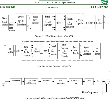
The OFDM transmitter section is illustrated in Figure 1. The MIMO-OFDM [14] section is grouped into two stages of data processing, the digital backend and digital front end. The digital backend module performs modulation such as QPSK or QAM, the output of modulator is space time encoded. In the digital front end module, the space time encoded data is transformed from frequency to time and is cyclic prefixed. The output of digital front end module is given to RF section for up conversion from IF to RF. The OFDM signal thus generated is then passed through a DAC before feeding it to the RF frontend section of the transmitter. It is then amplified to the required power levels to be transmitted. The transmitted signal is assumed to travel through a Gaussian noise channel, at the receiver the transmitted signal along with the noise is considered for demodulation.
de-Journal of Theoretical and Applied Information Technology 10th December 2013. Vol. 58 No.1
© 2005 - 2013 JATIT & LLS. All rights reserved.
ISSN: 1992-8645 www.jatit.org E-ISSN: 1817-3195 interleaved. The de-interleaved data is then passed
through the Viterbi decoder and then to the un-scrambler to recover the system input.
The OFDM signal is first de-serialized and then fed to the cyclic prefix removal system. After the cyclic prefix is attenuated from the OFDM signal, it is fed to the FFT section which de-maps the data from each of the subcarriers. This is then fed to the demodulator to recover the original data. The limitation of MIMO-OFDM systems is the increases in complexity of the receiver module as higher modulation schemes are used. In order to overcome the limitations of FFT based OFDM model, in this chapter NCO based OFDM module is proposed.
3. ARCHITECTURE FOR A MULTIBAND OFDM SYSTEM
One approach to design a UWB system based on OFDM is to combine the modulation technique with a multibanding approach [15], which divides the spectrum into several sub-bands, whose bandwidth is approximately 500 MHz [16], [17]. The transmitted OFDM symbols are time-interleaved across the subbands. An advantage of this approach is that the average transmitted power is the same as a system designed to operate over the entire bandwidth. Other advantages of multibanding include processing the information over much smaller bandwidth (approximately 500 MHz), which reduces power consumption and lowers cost, improving spectral flexibility and worldwide compliance. An example of a multiband OFDM TX and RX [18], [19] is shown in Figure 3 and Figure 4. The TX and RX architectures for a multiband OFDM system are very similar to that of a conventional wireless OFDM system. The main difference is that the multiband OFDM system uses a time–frequency kernel to specify the center frequency for the transmission of each OFDM symbol. An example of how the OFDM symbols are transmitted in a multiband OFDM is shown in Figure 5.
Figure 5 shows one realization of a time– frequency code, where the first OFDM symbol is transmitted on sub-band 1, and the second OFDM symbol is transmitted on sub-band 3, the third OFDM symbol is transmitted on sub-band 2, and fourth OFDM symbol is transmitted on sub-band 1, and so on. In practice, the time–frequency code can
be quite different and much longer in length. The
time–frequency codes are used not only to provide frequency diversity in the system, but also to
provide multiple accesses. From Figure 5, it is also apparent that a guard interval (9.5 ns) is appended to each OFDM symbol and that a CP is inserted before each OFDM symbol. The guard interval ensures that only a single RF transmit and RF RX chain are needed for all channel environments and all data rates and that there is sufficient time for the TX and RX to switch between the different center frequencies.
4. MBOFDM UWB FOR POWERLINE COMMUNICATIONS
MBOFDM UWB signals are very complex and hence generation of signals also leads to complexity. MBOFDM UWB generation has two parts, the first part generates MBOFDM UWB the second part down converts the generated signal to 50-578 MHz using discrete components of digital down converters. As the down converter is external to MBOFDM UWB flexibility in system adaptability is affected. The 128 subcarrier OFDM system covers a very wide frequency band while the power-line channel exhibits frequency-selective fading. It causes degradation of system performance. The existing MB-OFDM UWB system does not support adaptive modulation and power control. In this work an integrated system that integrates MBOFDM UWB with digital down converter is designed and modeled for PLCs. Figure 6 shows the proposed MBOFDM UWB system with digital down converter and up converter at the transmitter and receiver. The UWB signals generated with carrier frequencies fc = [3939 3978 4017 4056 3900 4094 7878 7956 8034 8112 7800 8190] MHz are down converted to
frequencies fplc = [53.3, 80, 106.6, 160, 200, 320,
400, 480, 528] MHz. It has been shown that this 528-MHz bandwidth can enable data transmission at rates of up to a gigabit per second even when the available signal power is very low [11], [12]. In this work, the MBOFDM UWB signals are down converted to 528 MHz using the direct digital synthesizer that generates the local oscillator signal
to translate the centre frequency fc to fplc. The input
Journal of Theoretical and Applied Information Technology 10th December 2013. Vol. 58 No.1
© 2005 - 2013 JATIT & LLS. All rights reserved.
ISSN: 1992-8645 www.jatit.org E-ISSN: 1817-3195 to produce output data. The received data is used to
compute Bit Error Rate (BER) to evaluate performance of MBOFDM UWB system. The UWB frequency of fc (3939 MHz) is converter to fplc (528 MHz) by using the LO (4467 MHz) by
using the expressions
The lower side band fc-LO is filtered using the band pass filter and is transmitted over PLC. At the receiver the lower side band signal is up converted using LO generated using the DDS. Figure 6 Proposed MBOFDM UWB with digital down converter and up converter for PLCs The upper side band is filtered and is taken through the UWB system to obtain the output data. Next section discusses the design and modeling of proposed MBOFDM UWB system with Digital Down Converter (DDC) and D Digital Up Converter (DUC) for PLC.
5. DESIGN AND MODELLING OF MB
OFDM UWB SYSTEM FOR PLC
The MB OFDM UWB system consists of a data Scrambler, Convolution Encoder, puncture, IFFT, GMSK Modulation, DAC, Channel, LPF, ADC, demodulation, Viterbi Decoder, Deinerleaver, and Descrambler. The DDC, DUC and DDS are interfaced to generate the UWB signals for PLC system.
5.1 Data Scrambler
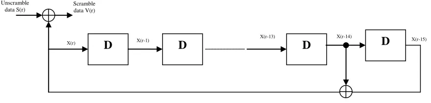
Scrambler shall be employed to support cryptography. The stream of downlink packets shall be randomized by modulo-2 addition of the data with the output of the pseudo-random binary sequence (PRBS) generator as illustrated in Figure 7 to decrease the Hamming distance between two strings of bits. Scrambler is used to uniformly redistribute the zeros and ones bits over the data input. The scrambler scheme, recommended by the IEEE 802.15 standard is presented on Figure 7. For the pseudo random binary sequence (PRBS) generator is
The initialization sequence,
where xin-k represents the binary initial value at the output of the kth delay element. The scrambled data bits vn, are obtained from unscrambled input bits sn,
by XORing , where sn represents the
unscrambled data bits. The side-stream de-scrambler at the receiver shall be initialized with the same initialization vector, xinit, used in the transmitter
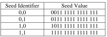
[image:4.612.325.512.139.205.2]scrambler. The initialization vector is determined from the seed identifier as given in Table 1.
Table 1: Scrambler Seed Selection
Seed Identifier Seed Value
0,0 0011 1111 1111 111
0,1 0111 1111 1111 111
1,0 1011 1111 1111 111
1,1 1111 1111 1111 111
5.2 Forward Error Correction Coding And Interleaving
The convolutional encoder is one type of Linear Error Control Codes used to encode data so that errors introduced due to noise in the channel can be corrected by the decoder. Two important characteristics of a convolutional encoder are its rate and constraint length. If k data bits are shifted in for every n encoded bits shifted out, the rate of the code equals k/n. If the maximum degree of the generator polynomials are m, then the constraint length of the code equals k(m+1). Figure 9 (a) shows the convolutional encoder and figure 9 (b) shows the Viterbi decoder architecture for hard decision logic.
The encoder's constraint length is a vector of length 2 because the encoder has two inputs. The elements of this vector indicate the number of bits stored in each shift register, including the current input bits. Counting memory spaces in each shift register in the diagram and adding one for the current inputs leads to a constraint length of [5 4]. To determine the code generator parameter as a 2-by-3 matrix of octal numbers, use the element in the ith row and jth column to indicate how the ith input contributes to the jth output. For example, to compute the element in the second row and third column, the leftmost and two rightmost elements in the second shift register of the diagram feed into the sum that forms the third output. Capture this information as the binary number 1011, which is equivalent to the octal number 13. The full value of the code generator matrix is [23 35 0; 0 5 13]. Figure 10 shows the convolutional encoder and Viterbi Decoder output of first 20 bits.
5.3 Bit Interleaving
Journal of Theoretical and Applied Information Technology 10th December 2013. Vol. 58 No.1
© 2005 - 2013 JATIT & LLS. All rights reserved.
ISSN: 1992-8645 www.jatit.org E-ISSN: 1817-3195 exploits frequency diversity across subcarriers and
provides robustness against narrow-band interferers.
5.4 IFFT
The MB OFDM symbols are generated by an IFFT operation with 128 points one advantage of IFFT is it saved the number of bank modulator. The idea behind IFFT is to generate orthogonally between MBOFDM symbols by multiplying different symbol with different frequency carrier, then sum those signals into one signal to transmit it to the channel. Figure 11 shows the OFDM using
IFFT. Input symbols from mapper [C1, C2, C3 ……
CN] that consists of phase-frequency information
are multiplied by orthogonal carriers of frequencies
f1 to fN and are combined to form OFDM signal. At
the receiver orthogonal carriers are used to extract
symbols from the received OFDM signal.
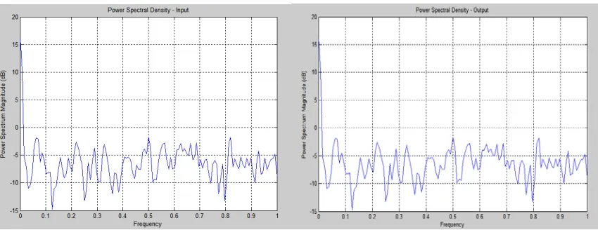
Sub-carriers modulation is performed after the IFFT process. In this work Gaussian Minimum Shift Key modulation is used, the advantage of GMSK over others modulation technique is that it has phase continuity. In MB approach, the spectrum is divided into 14 bands (each with a bandwidth equal to 528 MHz), and devices are allowed to statically or dynamically select which bands to use for transmission. The entire spectrum is divided into 4 distinct groups. Other groups have been reserved for future use. Figure 5 shows time-frequency coding for the MBOFDM system, where the first OFDM symbol is transmitted on sub-band 1, the second OFDM symbol is transmitted on sub-band 3, the third OFDM symbol is transmitted on sub-band 2, the fourth OFDM symbol is transmitted on sub-band 1, and so on [13].The Time Frequency Kernel to switch the center frequencies between three bands as shown in Figure 5. The receiver consists of LPF, ADC, Demodulation FFT, Deinterleaver, Viterbi decoder and descrambler. Figure 13 shows the MBOFDM UWB channel output and the filtered channel output at the
receiver.And also shows the power spectral density
of input signal, the input consists of DC component and hence the PSD is at its peak at zero frequency. Figure 14 shows Power spectral density of the input data which means the power of the signal before transmitting it. The observation shows that the spectrum lies from 0dB to -20 dB. Figure 14 The power spectral density of the output of the transmitter which is limited between-15db and-42 db as IEEE 802.15 standard to prevent interfere with others devices because UWB use unlicensed spectrum so that why it has less power compare to others devices by taking the PSD of the output.
The PSD of all harmonics is less than 15dB compared with the message signal. The normalized frequency is plotted against power spectral magnitude. The input signal is modulated using multiband OFDM technique and is transmitted to Noisy Channel. The received signal is demodulated and message is extracted. The output message demodulated and is compared with input PSD. From the comparison results shown it is found that the PSD resemble in both cases, thus ensuring the reconstruction capabilities of MIMO OFDM. Figure 15 shows the SNR vs BER performances of MBOFDM UWB. For SNR between -10 dB to 5 dB, BER is varying between
9e10-3 to 3e10-3 thus the BER remains constant for
SNR 15dB variation.
5.5 Design of DDC and DUC For MBOFDM UWB
Power Line Communication or Power Line Carrier (PLC), also known as Power line Digital Subscriber Line (PDSL), mains communication, Power Line Telecom (PLT), Power Line Networking (PLN), or Broadband over Power Lines (BPL) are systems for carrying data on a conductor also used for electric power transmission. Electrical power is transmitted over high voltage transmission lines, distributed over medium voltage, and used inside buildings at lower voltages. Power line communications can be applied at each stage. Most PLC technologies limit themselves to one set of wires (for example, premises wiring), but some can cross between two levels (for example, both the distribution network and premises wiring). Typically the transformer prevents propagating the signal so multiple PLC technologies are bridged to form very large networks. The block diagram of the DUC core is shown in Figure 16. The baseband signal is translated to desired channel using the DDS and mixer comprising the multipliers. The sample rate is adjusted to match the channel bandwidth. This is performed by the multistage multi-rate filter consisting of cascaded integrator comb filter interpolator. The full precision output of one stage is carried forward for processing by next stage. This will generate more number of bits at the output. Hence the full precision results of one stage would be reduced before it is processed. This is done by using Bias-free convergent rounding. This will be inserted after each CIC filters and mixer.
Journal of Theoretical and Applied Information Technology 10th December 2013. Vol. 58 No.1
© 2005 - 2013 JATIT & LLS. All rights reserved.
ISSN: 1992-8645 www.jatit.org E-ISSN: 1817-3195 stages CIC interpolation filters. A CIC filter
up-samples the output by a factor of 8. The up-sampled signal is now given to the multiplier as the first input. Variable DDS is used to generate carrier frequencies in the range of 4460 – 5100 MHz is given as a second input to the multiplier. This multiplier output is the up-converted signal. This DUC output is given as an input for DDC. The block diagram of the DDC Core is shown in Figure 17. The desired channel is translated to baseband using
the digital mixer comprising the multipliers and a
direct digital synthesizer (DDS).
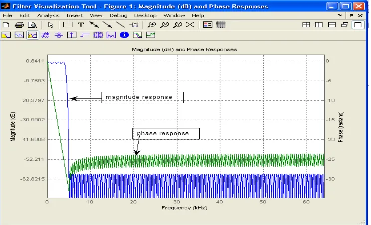
The sample rate of the signal is then adjusted to match the channel bandwidth. This is performed using a multi-stage multi-rate filter consisting of the cascaded integrator comb (CIC) filter decimator The full precision of a processing stage, i, may be carried forward for processing by stage i+1. Typically this would not be the case, and the full precision result of one stage would be reduced before it is processed by a subsequent stage. Bias-free convergent rounding is employed for this process. Figure 18 shows the MATLAB modeling of Digital Up Converter and the blocks are used to model. The output of sine wave block is taken as input for CIC interpolation filter. The block parameters of CIC interpolation are Interpolation factor of 8, Differential delay (M) of 1, number of sections of 3. The magnitude and phase response of CIC interpolation FIR filter is shown in Figure 18.
Compensation filter is a type of FIR filter used to compensate for loses in CIC filter in the typical interpolation filtering applications a reasonably flat pass band and narrow transition region filter performance is required. These desirable properties are not provided by the CIC filters alone, with their drooping pass band gains. The magnitude and phase response of CIC interpolation FIR filter is shown in
Figure 20.The decimal values at the output of DDC
in Simulink are taken. For these values, FFT (Fast Fourier Transformation) is calculated. X = [1529, 4012, 5859, 6784, 6688, 5573, 3598, 1050, 1688, -4171, -5988, -6912, -6816, -5701, -3726, -1179]. FFT is calculated in MATLAB by using
This is expressed in dB by
and the plot of Z is showing in Figure 21.
SNR is calculated by using From figure 5-15,
From Figure 21, THD is calculated by
From the THD value it is found that the harmonic component is not very dominant in the UWB system over PLC. The major challenges are the down conversion of 3939 MHz centre frequency to 528 MHz component as per PLC requirement. The down conversion leads to harmonics and sub components that need to be filtered using suitable filters that introduce minimum harmonics. On the other hand at the receiver side, the digital up converter need to up convert the signal from 528 MHz to 3939 MHz, which again introduces harmonics and sub components. The challenges in down conversion and up conversion are addressed in this paper by optimum design of CIC filters and PFIR filters. The frequency band for PLC between 50 MHz to 578 MHz need to be reconfigurable, hence there is need for reconfigurable DDC which need to be designed as LO module.
6. CONCLUSION
In this paper, MBOFDM UWB system is integrated with digital down converter at the transmitter and digital up converter at the receiver to design an integrated system that can be used to transmit data over power line. The designed system supports data rate in the range of 50Mbps to 500Mbps, the input data is translated to UWB frequency in the range between 3939 MHz to 8190 MHz and is further down converted to the range 50 MHz to 578 MHz for power line requirement. The system is modeled using Matlab and Simulink, the interfaced system is simulated for various test cases of input data. BER performance is estimated and is
found to be 10-3. The digital up converter and down
converter are designed using CIC and PFIR filters to minimize harmonic distortion, THD is found to be of 1.2. The design is suitable for power line communication; FPGA implementation of the proposed system would provide detailed information on hardware complexities and feasibility for real time applications.
REFRENCES:
[1] ITU Recommendation G.9960, “Unified
high-speed wireline based home networking transceivers Foundation. Oct. 2009.
[2] IEEE P1901 Draft Standard, Broadband over
Power Line Networks: Medium Access Control and Physical Layer Specifications. Jan. 2010.
[3] N. Pavlidou, A. H. Vinck, J. Yazdani, and B.
Journal of Theoretical and Applied Information Technology 10th December 2013. Vol. 58 No.1
© 2005 - 2013 JATIT & LLS. All rights reserved.
ISSN: 1992-8645 www.jatit.org E-ISSN: 1817-3195
the art and future trends”, IEEE Commun.
Mag.,vol. 41, no. 4, Apr. 2003, pp. 34–40.
[4] A. Majumder and J. Caffery, “Power line
communications: An overview”, IEEE
Potentials, vol. 23, no. 4, Oct./Nov. 2004 ,pp.
4–8.
[5] HomePlug Powerline Alliance, HomePlug AV
White Paper. [Online]. Available: http://www.homeplug.org
[6] Oppermann, M. Hamalainen, and J. Iinatti,
UWB: Theory and Applications. Hoboken, NJ:
Wiley, Sep. 2004
[7] FCC Report and Order, “In the matter of
revision of Part 15 of the Commission’s rules regarding ultrawideband transmission systems”, Apr. 2002. Commision of the European Communities, “Commission decision on allowing the use of the radio spectrum for equipment using ultra-wideband technology in a harmonised manner in the community”, Feb. 2007
[8] Ofcom, “Decision to make the wireless
telegraphy (ultra-wideband equipment) (exception) regulations 2007,” Aug. 2007.
[9] Mekuria and H. Hirsch, “UWB pulse
transmission over powerline channel”,
presented at the Int. Symp. Powerline Commun.
Appl. (ISPLC), Pisa, Italy, Apr. 2007.
[10] A. Tonello, “Wideband impulse modulation and receiver algorithms for multiuser powerline
communications”, EURASIP J. Advances Signal
Process., vol. 2007, Mar. 2007, pp. 1–14.
[11] S. Chen, X. Chen, and C. G. Parini, “Measurement and simulation of powerline channel using OFDM for UWB
communication”, in Proc. IEEE Int. Conf.
Powerline Commun. Appl., Dresden, Germany,
Mar. 2009, pp. 79–84.
[12] S. Chen, M. Setta, X. Chen, and C. G. Parini, “Ultra wideband powerline communication
(PLC) above 30 MHz”, IET Commun., vol. 3,
no. 10, Oct. 2009, pp. 1587–1596.
[13] S. Chen, M. Magani, X. Chen, and C. G. Parini, “Exploit adaptive modulation in UWB powerline communication for improved BER
performance”, in Proc. IEEE Int. Symp.
Powerline Commun. Appl., Rio de Janeiro,
Brazil, Mar. 2010, pp. 195–200.
[14] S. Masood Ur Rehman, Shihua Wang, Yanchao Liu, Shuxian Chen, Xiaodong Chen and Clive
G. Parini, “Achieving High Data Rate in
Multiband-OFDM UWB Over Power-Line
Communication System”, IEEE Transactions
On Power Delivery, Vol. 27, No. 3, July 2012,
pp. 1172-1177.
[15] Alfred Grau., Hamid Jafarkhani. and Franco De Flaviis, “A Reconfigurable Multiple-Input
Multiple-Output Communication System”,
IEEE Transactions on Wireless
Communications, Vol. 7, No. 5, May 2008.
[16] Bruno Bougard., Gregory Lenoir., Antoine Dejonghe., Liesbet Van der Perre, Francky Catthoor. and Wim Dehaene, “SmartMIMO: An Energy-Aware AdaptiveMIMO-OFDM Radio Link Control for Next-GenerationWireless
Local Area Networks”, EURASIP Journal on
Wireless Communications and Networking,
2007.
[17] Kaiser, T., Wilzeck, A., Berentsen, M. and Rupp, M., “Prototyping for MIMO systems- an
overview”, Proceedings of 12th European
Signal Processing Conference (EUSIPCO '04),
Vienna, Austria, September 2004 pp. 681 to 688.
[18] Batra, A., et al. , “Multi-band OFDM physical
layer proposal”, IEEE P802.15-
03/268r0-TG3a, July 2003.
[19] Veena M.B. and M.N. Shanmukha swamy “Implementation of MIMO-OFDM front end
model on FPGA”, IJEST, Vol, No 2, Feb
2011,pp 1159-1166.
[20] A. Batra, J. Balakrishnan, and G. R. Aiello, “Design of a multiband OFDM system for
realistic UWB channel environments”m IEEE
Trans.Microw. Theory Techn., vol. 52, no. 9,
Sep. 2004, pp. 2123–2138.
[21] Working with Convolutional Encoder and
Viterbi Decoder, www.mathworks.in/matlabcentral/fileexchange/
.../38559-viterbi-decoder
[22] Cyril Prasanna Raj and Subash, “Design of Digital Up Converter and Digital Down
Converter”, SASTech Journal, Vol.1, 2007,
Journal of Theoretical and Applied Information Technology 10th December 2013. Vol. 58 No.1
© 2005 - 2013 JATIT & LLS. All rights reserved.
ISSN: 1992-8645 www.jatit.org E-ISSN: 1817-3195
Figure 1: OFDM Transmitter Using IFFT
[image:8.612.91.529.54.457.2]Figure 2: OFDM Receiver Using FFT
Figure 3: Example TX Architecture for a Multiband OFDM System
Figure 4: Example RX Architecture for a Multiband OFDM System Scramble
r
Convolutio nal Encoder
Punctur er
Bit Interleave
Constellati on
IFFT /
DA C
Time-frequency Input
data
LPF VGA ADC FFT Deinterleaver Decoder Viterbi Descrambler
Output Data
LPF VGA ADC FFT Deinterleaver Decoder Viterbi Descrambler
Output Data Time-frequency kernel
Journal of Theoretical and Applied Information Technology 10th December 2013. Vol. 58 No.1
© 2005 - 2013 JATIT & LLS. All rights reserved.
[image:9.612.90.481.70.244.2]ISSN: 1992-8645 www.jatit.org E-ISSN: 1817-3195
[image:9.612.90.551.290.520.2]Figure 5: Example of Time-Frequency Coding For the Multiband OFDM System
Figure 6: Proposed MBOFDM UWB with digital down converter and up converter for PLCs
Figure 7: Realization of the Randomizer Linear Feedback Shift Registers [9]
D
D
D
D
Unscramble data S(r)
Scramble data V(r)
X(r) X(r-1)
X(r-13) X(r-14)
X(r-15)
Output Data
Viterbi decoder
Depuncture/ Bit interleave
De-modulation
or mapping FFT
Cyclic prefix
Multiplier
Time-frequency kernel (fc)
Digital up converter
Direct digital synthesizer (LO)
Power Line (fplc)
Input Data
Conv. Encoder
Puncture/ Bit interleave
Modulation or mapping
IFFT Cyclic prefix
Multiplier
Time-frequency kernel (fc)
Digital down converter
Direct digital synthesizer (LO)
Power Line (fplc)
Channel 1
Channel 2
Channel 3
Frequency (MHz)
3168
3696
4224
4752
9.5 ns Guard Interval for Tx/Rx
312.5 ns
60.6 ns
Period = 937.5 ns
[image:9.612.98.538.559.664.2]Journal of Theoretical and Applied Information Technology 10th December 2013. Vol. 58 No.1
© 2005 - 2013 JATIT & LLS. All rights reserved.
[image:10.612.89.525.71.253.2]ISSN: 1992-8645 www.jatit.org E-ISSN: 1817-3195
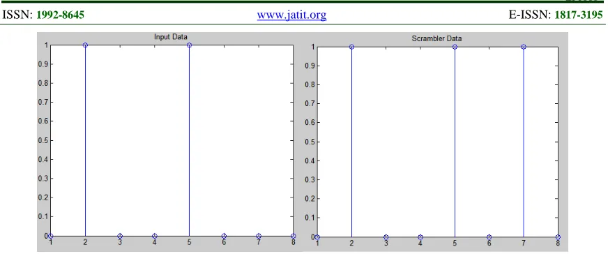
Figure 8: Input Data and Scrambled Output Data
Figure 9 (a) Convolution Encoder with a Rate 3/2
[image:10.612.195.456.309.458.2] [image:10.612.154.460.513.678.2]Journal of Theoretical and Applied Information Technology 10th December 2013. Vol. 58 No.1
© 2005 - 2013 JATIT & LLS. All rights reserved.
[image:11.612.97.524.70.237.2]ISSN: 1992-8645 www.jatit.org E-ISSN: 1817-3195
[image:11.612.92.511.293.662.2]Figure 10: Convolution Encoder and Viterbi Decoder Output
Figure 11: Multi Carrier Modulation Using IFFT
Figure 12: IFFT and FFT Output
C1
C2
CN
-Cos (W1) Cos (W1)
Cos (W2)
Cos (WN)
∑
-Cos (W2)
-Cos (WN) Channel
C’1
C’2
Journal of Theoretical and Applied Information Technology 10th December 2013. Vol. 58 No.1
© 2005 - 2013 JATIT & LLS. All rights reserved.
[image:12.612.91.520.72.270.2]ISSN: 1992-8645 www.jatit.org E-ISSN: 1817-3195
[image:12.612.96.521.294.458.2]Figure 13: Channel Output and LPF Output at the Receiver
Figure 14: Power Spectral Density Of Input And Output Data
[image:12.612.166.449.480.714.2]Journal of Theoretical and Applied Information Technology 10th December 2013. Vol. 58 No.1
© 2005 - 2013 JATIT & LLS. All rights reserved.
[image:13.612.102.514.63.684.2]ISSN: 1992-8645 www.jatit.org E-ISSN: 1817-3195
[image:13.612.95.515.67.363.2]Figure 16: DUC Block Diagram [21]
Figure 17: DDC Block Diagram [21]
Figure 18: MATLAB Modeling Of DUC
CIC
4
Input signal
50-
CIC
2
DDS
Up converted Signal
Output
signal
To PLC
DDS
4460-5100
Input signal
3939-8190
CIC
4
[image:13.612.125.489.424.671.2]Journal of Theoretical and Applied Information Technology 10th December 2013. Vol. 58 No.1
© 2005 - 2013 JATIT & LLS. All rights reserved.
[image:14.612.97.524.65.348.2]ISSN: 1992-8645 www.jatit.org E-ISSN: 1817-3195
Figure 19: Magnitude And Phase Response Of CIC Interpolation Filter
[image:14.612.122.494.413.639.2]Journal of Theoretical and Applied Information Technology 10th December 2013. Vol. 58 No.1
© 2005 - 2013 JATIT & LLS. All rights reserved.
[image:15.612.89.526.68.347.2]ISSN: 1992-8645 www.jatit.org E-ISSN: 1817-3195

![Figure 16: DUC Block Diagram [21]](https://thumb-us.123doks.com/thumbv2/123dok_us/8914241.960915/13.612.125.489.424.671/figure-duc-block-diagram.webp)