LOW POWER IN NANO-SCALE CMOS MEMORY
LABONNAH F. RAHMAN, F. B. ARITH, M. I. B. IDRIS, M. B. I. REAZ, MOHD. MARUFUZZAMAN
Department of Electrical, Electronic and Systems Engineering, University Kebangsaan Malaysia,
43600, UKM, Bangi, Selangor, Malaysia E-mail: [email protected]
ABSTRACT
Future technologies required nano-scale CMOS memory to be operating in low power consumption. The minimum operating voltage of the nano-scale CMOS played as a main factor to reduce the power consumption. Consequently, there are some limitations and obstacles to achieve the objective for several design, material and novel structural solutions, which are promising and reliable. In this research, the noticeable limits, possible annexes and applications of CMOS technologies in the nanometer regime is discussed. This paper mainly describes the limitations that conventional MOSFET is faced. In addition, the solutions to low power in nano-scale CMOS memory are presented. Therefore, analysis of the attainable performance and potential restrictions of CMOS technologies from the point of design, material and structural solution techniques are illustrated.
Keywords: Nano-Scale, CMOS, Low Power, Memory
1.
INTRODUCTIONIn modern world, Integrated circuit (IC) is an advanced electric circuit by patterned diffusion of trace elements into the thin surface of a semiconductor material. All electronic equipment today is used IC and it has revolutionized the world of electronics [1-8]. Due to the introduction of complex metal oxide semiconductor (CMOS) technology, semiconductor devices spread through every discipline of engineering and CMOS memories become core component [9-15]. Memory cells are the essential part of semiconductor memory ICs. The features of memory cells are extensively affect the chip size, operational speed and power dissipation of memory devices. In very large scale integration (VLSI) technology, memories developed in CMOS process are utilized in a number of applications as the sources of store data in RFID applications [16-23]. Basic examination of the memory cells comprises structural, storage-mechanism, write, read, and design and improvement issues. Generally, a memory cell, which is applicable to CMOS memory designs, comprises a data storage circuit; one or more data access devices. Additionally, some designs have additional circuit elements. Almost all CMOS memories, one storage circuit or element is capable to hold one bit of binary information, but some storage elements are able to
store a multiplicity of binary or non-binary data. Additional circuit elements may be used to improve environmental tolerance and to accommodate a variety of functions in a single memory cell.
In nano-scale CMOS memory, reducing minimum operation voltage Vdd is becoming very
difficult to do in conventional bulk CMOS. The limitation in low-voltage Vmin is one of the major
problems [23-26]. As the technology of device minimization is increased, various effects such as delay, voltage margin of circuit, significantly increased in soft error rates, Vmin etc also increased,
Vdd must be increased with device scaling to offset
such effects, which causes an increase in the power dissipation, as well as degrades the device reliability due to increased stress voltage [27-30]. Due to such inherent features of Vt0 and Vth, Vdd is
facing a 1V wall in the 65 nm generation, and is expected rapidly increase with further scaling of poly-Si bulk MOSFETs as shown in Figure 1 [24, 26]. To reduce the operating voltage Vdd, the
minimum operating power supply Vdd (i.e Vmin) as
determined by Vt0 and Vth must be reduced. This is
because Vdd is the sum of Vmin and ∆, and Vmin
becomes much higher than ∆ in the nano-scale era. Here, ∆is the sum of the power-supply droop and noise in the power supply lines and substrate, the voltage needed to compensate for the extrinsic
∆due to short-channel effects and line-edge
speed target. In any event, for the LSI industry in order to flourish and proliferate, the 1V wall must be breached in the nano-scale era.
Figure 1. Trends In Vdd And Vmin Of High-Performance Mpus [24,26]
The lowest necessary threshold voltage
of MOSFETs and the ever-increasing variation
are factors that cause to increase.Due to the
variations in , various problems occur, such as
delay or wider variations in circuit speed, degradation of voltage margins of flip-flops and increased soft-error rates (SER) in RAM cells and logic rates [31-32]. Therefore, clarifying and solving the increasingly critical Vmin problem is
extremely important in our future.
This paper mainly describes the limitations that conventional MOSFET had and the solutions to low power the CMOS memories. These can be divided into three points of view. The first one is circuit design continue by material and finaly is the new structure of MOSFETs.
2.
BACKGROUNDIf is defined as , which is necessary for
achieving a tolerable speed variation ∆, is given
as[1-9]:
1 ∆,
1/∆
. 1,
∆ (1)
.
, and ∝ (2)
where, is an average with a maximum
deviation in from, is the standard
deviation of distribution, and the speed variation
is defined as the ratio of the slowest speed at thehighest to the average speed at the
average ≅ . For a conventional, bulk
MOSFET
/
.
∝
.
.
(3)
where m depends on the circuit count in the block, and are the Pelgrom and Takeuchi
constants, respectively, is the inversion electrical gate-oxide thickness, is the flat-band voltage,
Φis the surface potential, is the impurity
concentration of the channel, and LW is the MOSFET size [33-34].
In order to reduce minimum voltage with
smaller especially for low-power designs, the
resultant leakage must be reduced dramatically. Therefore, two ways has been discussed in term of design technique solution, which are low minimum voltage and structural of operation. These
solutions were applied on 6T SRAM type that is one type of CMOS memory.
By applying low minimum voltage the
power consumption of the whole cell can be reduce [35-36]. The required voltage, which indicated as,
is very sensitive to the threshold-voltage
variations . It significantly related with device
scaling, and to the lowest threshold voltage,, of
the cell. For example by reducing the supply voltage of the 6T, SRAM cell leads to the low
leakage currents [37-38]. These leakage currents occur due to the electric fields that contains inside the cell. Consequently, the lower minimum voltage
applied to the cell the lesser voltage that
the cell required [39].
Figure 2. Memory cell with read and write circuitry [40]
There are also some other solution which by replacing the material of the CMOS. Hybrid-Graphene-Nanoribbon CMOS and Josephson-CMOS Hybrid memory has been widely discussed by researchers lately. These future technologies seem promises to reduce the power consumption as well as high-speed operation system.
Graphene produce special electrical properties seem to replace conventional CMOS material as Silicon technology move towards scaling limitation [44]. Previously several Graphene mainly electronic devices and interconnects have been proposed.
Figure 3. Proposed Graphene-CMOS Fabric (a) Layout Top View (b) Graphene Layer (c) 3D Integration between
CMOS and Graphene [44]
The possibility of a hybrid fabric between CMOS and Graphene by implementing a novel Graphene Nanoribbon crossbar (xGNR) based volatile tunneling RAM (GNT RAM) and integrating it with the 3D CMOS stack and layout has been designed and is shown in Figure 3. Evaluation detailed of GNT RAM circuits show that they have reliable advantages in terms of power consumption, area and write performance over 16nm CMOS. This effort enlightens new idea other possibilities including multi-state memory fabrics and even an all-graphene fabric promises future technology.
[image:3.612.110.262.440.680.2]A 64-kb Josephson–CMOS hybrid random-access memory (RAM) has been designed using ultrafast hybrid interface circuits, which is shown in Figure 4. The milli volt-level Josephson signals are amplified to volt-level CMOS digital signals by a hybrid interface amplifier. By minimizing the parasitic capacitance load, the performance of this amplifier is improved [45]. The 4-K operation of short-channel CMOS devices and circuits show some promises consequences. The memory bit-line output currents are detected by ultralow-power high-speed Josephson devices. As results the first high-frequency access time measurements on the full critical path showing 600 pS for a single bit. Therefore, the design can reduce the crosstalk and improve margins leads the reduction power dissipation and latency.
Figure 4. Hybrid memory system of 64 kb for measuring delays including overall access time for single cell [45]
[image:3.612.346.502.464.581.2]a number of further research and as well as manufacturing cost.
In our challenges to reduce voltage (), we
realize that there is a limitation in a bulk-MOSFETs. An ultra-small voltage will not be achieved if we keep using the bulk-MOSFET. Thus, for compensation circuit and new device with small variation of is required. The new device
must be suitable for low-voltage operation, such as small-for small and scalable MOSFETs. For
these challenges, FD-SOI and FinFET will be indispensable even though it is high in cost.
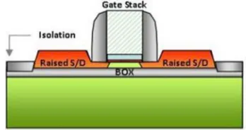
In order to minimize, FD-SOI MOSFETS
[image:4.612.317.520.103.183.2]is the most important device [46]. Figure below shows the structure of FD-SOI MOSFET.
Figure 5. Planar of FD-SOI MOSFET [46] FD-SOI is expected to reduce the variation of
to half or more. For example, if only the FD-SOI is used, the in the 32-nm generation is reduced
from 1.47 V to 0.93 V for SRAMs, 0.85 V to 0.58 V for logic gates, and 0.50 V to 0.35 V for DRAMs[47]. This device has small and can
reduced short channel effect (SCE), body effect, afford a small SER etc. effectively [47-48]. Besides that, we can control the value of by changing
the doping of the substrate under the UT-BOX layer. Moreover, FD-SOI with high-k metal gate will enable smaller variation of [46].
Instead of using FD-SOI as a solution, FinFET also enable to reduce. Figure 6 show the
[image:4.612.106.280.332.424.2]FinFET structure. A FinFET transistor is forming a double-gate structure. This device is called “finfets” because the source/drain region forms fins on the silicon surface. Generally, Double gate FET can reduce short channel effects and FinFET is the easiest one to fabricate [49]. What makes FinFET special is because we can use of an ultra low-dose channel and a wide-channel built-in structure [23, 26, 49].
Figure 6. FinFET structure
Thus, it achieves not only a higher density and higher drive current but scalable (Vt) with
up-scaling of the fin height (that is, channel width W) despite channel length L being scaled down. For an example, in 11-nm device generation(DRAM), basis on the MOSFET scaling, we can predict the
for HP design using FinFET manage to reduce
until 0.22 V and for LP designs FinFET afford to reduce around 0.46 V[50].
However, the use of FD-SOI and FinFETs may also have some disadvantages. Besides the cost problem, the incremental of variation among dies is occurring as well. This would impose a need for stringent control of shape uniformity on the FinFET, which will make the process of fabrication more complex.
3. DISCUSSION
Conventional MOSFETs will soon reach the limit of low-voltage owing to the increasing
variation. Several techniques have been proposed in term of design, material and structure solution. Nevertheless, these approaches have some limitation and suppose to be investigated in the future. Furthermore, it is essential to use the new MOSFET such as FD-SOI and FinFETs in CMOS memory. These new MOSFETs have advantages in having low despite being miniaturized. This
characteristic is important and very useful in low-power nano-scale devices. However, the new MOSFET is not able to compete with the conventional MOSFET because of high cost in production.
4. CONCLUSION
structural include FD-SOI and FinFETs as a good alternative solution moving towards the future technologies.
REFRENCES:
[1] [1] M. Akter, M. B. I. Reaz, F. Mohd-Yasin, F. Choong, A modified-set partitioning in hierarchical trees algorithm for real-time image compression, Journal of Communications Technology and Electronics, Vol. 53, No.6, 2008, pp.642-650.
[2] Mogaki, S., Kamada, M., Yonekura, T., Okamoto, S., Ohtaki, Y., & Reaz, M. B. I., Time-stamp service makes real-time gaming cheat-free, in Proc. of 6th ACM SIGCOMM workshop on Network and system support for games, ACM, Sep. 2007, pp. 135-138.
[3] Mohd-Yasin, F., Khaw, M. K., & Reaz, M. B. I., Radio frequency identification: Evolution of transponder circuit design, Microwave journal, 49(6). pp. 56-70, 2006.
[4] Uddin, J., Reaz, M. B. I., Hasan, M. A., Nordin, A. N., Ibrahimy, M. I., & Ali, M. A. M., UHF RFID antenna architectures and applications, Scientific Research and Essays, 5(10), pp.1033-1051, 2010.
[5] Uddin, M. J., Ibrahimy, M. I., Reaz, M. B. I., & Nordin, A. N., Design and application of radio frequency identification systems, European Journal of Scientific Research, 33(3), pp.438-453, 2009.
[6] Choong, F., Reaz, M. B. L., Chin, T. C., & Mohd-Yasin, F., Design and implementation of a data compression scheme: A partial matching approach, in Proc. of the Computer Graphics, Imaging and Visualisation: Techniques and Applications, Sydney, Australia, July 26-28 2006, pp. 150-155.
[7] Choong, F., Reaz, M. B. I., & Mohd-Yasin, F., Power quality disturbance detection using artificial intelligence: A hardware approach, in Proc. of the 19th IEEE International Parallel and Distributed Processing Symposium (IPDPS 05), 04-08 Apr. 2005, pp. 146a.
[8] Reaz, M. B. I., Mohd-Yasin, F., Sulairnan, M. S., Tho, K. T., & Yeow, K. H., Hardware prototyping of boolean function classification schemes for lossless data compression, in Proceedings of the 2nd IEEE International Conference on Computational Cybernetics, Vienna, Austria, 2004, pp. 47-51.
[9] Reaz, M. B. I., Sulaiman, M. S., Yasin, F. M., & Leng, T. A, IRIS recognition using neural
network based on VHDL prototyping, in Proc. of the 2004 International Conference on Information and Communication Technologies: From Theory to Applications, 19-23 Apr. 2004, pp. 463-464
[10] Pang, W. L., Reaz, M. B. I., Ibrahimy, M. I., Low, L. C., Mohd-Yasin, F., & Rahim, R. A., Handwritten character recognition using fuzzy wavelet: A VHDL approach, WSEAS Transactions on Systems, 5, pp. 1641-1647, 2006.
[11] Assim, A., Reaz, M. B. I., Ibrahimy, M. I., Ismail, A. F., Choong, F., & Mohd-Yasin, F., “An AI based self-moderated smart-home”, Informacije MIDEM, 36, pp. 91-94, 2006. [12] Reaz, M. B. I., Leong, P. W., Mohd-Yasin, F.,
& Chin, T. C., Modeling of data compression using partial matching: A VHDL approach, in Proceedings of the 6th World Wireless Congress, (WWC 2005), San Francisco Bay Area, USA, 2005, pp. 411-416.
[13] Mamun, I. R., Lee, W. F., Hamid, N. H., Lo, H. H., Yeon, A., & Mohd. S., High degree of testability using full scan chain and ATPG-An industrial perspective, Journal of Applied Sciences, 9(14), pp. 2613-2618, Feb. 2009. [14] Teh, Y. K., Mohd-Yasin, F., Choong, F., Reaz,
M. I., & Kordesch, A. V., Design and analysis
of UHF micropower CMOS DTMOST
rectifiers, IEEE Transactions on Circuits and Systems II: Express Briefs, 56(2), pp. 122-126, 2009.
[15] Mohd-Yasin, F., Yap, M. T., & Reaz, M. B. I., CMOS instrumentation amplifier with offset cancellation circuitry for biomedical application, WSEAS Transactions on Circuits and Systems, 6(1), pp. 171-174, 2007.
[16] Alam, M. R., Reaz, M. B. I., & Ali, M. A. M., Statistical modeling of the resident's activity interval in smart homes, Journal of Applied Sciences, 11, pp. 3058-3061, 2011.
[17] L. F. Rahman , M. B. I. Reaz , M. A. M. Ali, M. Marufuzzaman, M. R. Alam, Beyond the WiFi:Introducing RFID system using IPv6, Proceedings of the ITU-T Kaleidoscope Conference, Pune, India, December 13-15 2010, pp. 1-4.
[18] Mohd-Yasin, F., Khaw, M. K., & Reaz, M. B. I., Techniques of RFID systems: Architectures and applications, Microwave Journal, 49(7), pp. 62-74, 2006.
IEEE International SOC Conference, Herndon, VA, 19-23 Sept. 2005, pp. 161-164.
[20] Khaw, M. K., Mohd-Yasin, F., & Reaz, M. L., Recent advances in the integrated circuit design of RFID transponder, in Proc. of the 2004 IEEE International Conference on Semiconductor Electronics, 7-9 Dec. 2004, pp. 326-330. [21] L. F. Rahman, M. B. I. Reaz, M. A. Mohd. Ali,
and M. Kamada, "Design of an EEPROM in RFID tag: Employing mapped EPC and IPv6 address," in Proc. of the IEEE Asia-Pacific Conference on Circuits and Systems, (APCCAS 2010), Kuala Lumpur, Malaysia, December 6-9, 2010, pp. 168-171.
[22] L. F. Rahman, M. B. I. Reaz, M. A. M. Ali, M. Marufuzzaman, “Implementation of Sense Amplifier in 0.18 µm CMOS Process”
Electronics and Electrical Engineering, Vol. 4, No. 120, 2012, pp. 113-116.
[23] B. S. K. Itoh, “Adaptive Circuit for the 0.5-V Nanoscale CMOS Era”, IEICE Transactions on Electronics, Vol. E93-C, No. 2, 2010, pp.216-233.
[24] K. Itoh, M. Horiguchi, M. Yamaoka, “Low-voltage limitations of memory-rich nano-scale CMOS LSIs”, Proceedings of 37th European Solid State Device Research Conference, September 11-13, 2007, pp.68-75.
[25] K. Itoh, M.Horiguchi, and H. Tanaka, “Ultra-Low Voltage Nano-Scale Memories,” Springer, Tokyo, Japan, 2007, pp. 346.
[26] K. Itoh, M.Yamaoka and T. Oshima, “Adaptive Circuits for the 0.5-V Nanoscale CMOS Era”, IEICE Trans. Electron., Vol. 93, No. 3, 2010, pp. 216-233.
[27] K. Itoh, K.Osada, and T. Kawahara, “Reviews and Prospects of low voltage embedded RAMs”, CICC 2004 Dig. Tech. Papers, October 2004, pp. 339-344.
[28] K. Itoh, “Low-Voltage Embedded RAMs in the Nanometer Era”, Proceedings of ICICDT, 2005, pp. 235-242.
[29] K. Itoh, M.H., and H. Tanaka, “VLSI Memory Chip Design”, Springer-Verlag, 2001, pp. 495. [30] Y. Nakagome, M. Horiguchi, T. Kawahara, K.
Itoh, K., “Review and prospects of low-voltage RAM circuits”, IBM Journal of Research and Development, Vol. 47. No. 516, Sep. /Nov. 2003, pp. 525-552.
[31] N. Seifert, B. Gill , V. Zia, M. Zhang and V. Ambrose," On the scalability of redundancy based SER mitigation schemes," Proceedings of
Int'l Conf. IC Design Tech, ICICDT 2007 Dig, May 2007, pp. 1-9.
[32] P. Shivakumar, M. Kistler, W. Keckler, D. Burger, and L. Alvisi. “Modeling the effect of technology trends on the soft error rate of combinational logic”, Proceedings of Int’l Conf. on Dependable Systems and Networks, 2002, pp. 389–398.
[33] M. J. M. Pelgrom, A. C. J. Duinmaijer, and A. P. G. Welbers," Matching properties of MOS transistors”, IEEE JSSC, Vol. 24, October 1998, pp. 1433 - 1439.
[34] K. Takeuchi, T. Fukai, T. Tsunomura, A. T. Putra, A. Nishida, S. Kamohara, and T. Hiramoto, "Understanding Random Threshold Voltage Fluctuation by Comparing Multiple Fabs and Technologies”, International Electron Devices Meeting, Washington D. C., USA, December 11, 2077, pp. 467 - 470.
[35] K. Itoh, “Low-Voltage Memory-Rich Nanoscale CMOS LSIs –Current Status and Future Trends,” Proceedings of 10th IEEE International Conference, 1-4 November 2010, Shanghai, 2010, pp.25-28.
[36] K. Itoh. M. Horiguchi. M. Yamaoka, “Low-Voltage Limitations of Memory Rich Nano-Scale CMOS LSIs,” Proceedings of 33rd European Solid State Circuit Conference, Munich, September 11-13, 2007, pp. 68-75. [37] O. Thomas, M. Belleville, R. Ferrant, “SRAM
Memory Cell Leakage Reduction Design Techniques in 65nm Low Power PD-SOI CMOS,” Proceedings of IEEE International Conference on Integrated Circuit Design and Technology and Tutorial (ICICDT 2008), Austin, TX, Jun 2-4, 2008, pp.51-54.
[38] K. Zhang, F. Hamzaoglu, and Y. Wang,
“Low-Power SRAMs in Nanoscale CMOS
technologies”, IEEE Transactions on Electron Devices, Vol. 55, No. 1, 2008, pp. 145-151. [39] Y. Frans, R. Schmitt, N. Nguyen ; S. Bhardwaj,
and G. Bronner, “Design Challenges of Low-Power and High-Speed Memory Interface in Advanced CMOS Technology,” Proceedings of Symposium on VLSI Technology Digest of Technical Papers, Honolulu, HI, Jun 14-16, 2011.
[41] B. D. Yang, “A Low-Power SRAM Using Bit-Line Charge-Recycling for Read and Write Operations”, Vol. 45, No. 10, 2010, pp. 2173 - 2183.
[42] M. H. Chi, W. HanMing, “Technologies and Materials for Memory with Full Compatibility to CMOS”, Proceedings of 9th International Conference on Solid-State and Integrated-Circuit Technology, Beijing, China, October 20-23, 2008, pp.823-826.
[43] P. Meinerzhagen, S.M.Y.Sherazi, A. Burg, J. N. Rodrigues, “Benchmarking of Standard-Cell Based Memories in the Sub-V_t Domain in 65nm CMOS Technology,” IEEE Journal on Emerging and Selected Topics in Circuits and Systems, Vol. 1, No. 2, 2011, pp. 173-182. [44] S. Khasanvis, Habib, K.M. Masum, M.
Rahman, P. Narayanan, R. K. Lake, C. A. Moritz, “Hybrid Graphene Nanoribbon-CMOS Tunneling Volatile Memory Fabric,” in Proc. of IEEE International Symposium on Nan scale Architectures (NANOARCH), San Diego, CA, Jun 8-9, 2011, pp. 189-195.
[45] K. Fujiwara, Q. Liu, T. Van Duzer, X. Meng, “New Delay-Time Measurements on a 64-kb Josephson-CMOS Hybrid Memory With a 600ps Access Time”, IEEE Transactions on Applied Superconductivity, Vol. 20, No. 1 , 2009, pp.1051-8223.
[46] R. Tsuchiya, N. Sugii, T. Ishigaki, Y. Morita, H. Yoshimoto, K. Torii, and S. Kimura, “Low Voltage (Vdd~0.6V) SRAM Operation Achieved by Reduced Threshold Voltage Variability in SOTB(Silicon on Thin BOX),” VLSI Tech Dig, June 2009, pp. 150-151. [47] K. Itoh, “Voltage Limitations and Challenges of
Memory-Rich Nano-Scale CMOS LSI”Low, Proceedings of 9th International Conference on Solid-State and Integrated-Circuit Technology, Beijing, China, October 20-23, 2008, pp. 739-742.
[48] H. Gotou, “Future bipolar device structures”,IEDM Gig. 1987.
[49] K. Itoh, N. Sugii, D. Hisamoto, and R. Tsuchiya, “FD-SOI MOSFETs for the Low-Voltage Nanoscale CMOS Era”, Proceedings of IEEE Int'l SOI conference, Foster City, CA , Oct. 2009,pp. 1-4.
![Figure 1. Trends In Vdd And Vmin Of High-Performance Mpus [24,26]](https://thumb-us.123doks.com/thumbv2/123dok_us/8913595.960589/2.612.102.283.130.330/figure-trends-vdd-vmin-high-performance-mpus.webp)
![Figure 2. Memory cell with read and write circuitry [40]](https://thumb-us.123doks.com/thumbv2/123dok_us/8913595.960589/3.612.346.502.464.581/figure-memory-cell-read-write-circuitry.webp)