N A N O E X P R E S S
Open Access
Radial n-i-p structure SiNW-based microcrystalline
silicon thin-film solar cells on flexible stainless
steel
Xiaobing Xie
*, Xiangbo Zeng, Ping Yang, Hao Li, Jingyan Li, Xiaodong Zhang and Qiming Wang
Abstract
Radial n-i-p structure silicon nanowire (SiNW)-based microcrystalline silicon thin-film solar cells on stainless steel foil was fabricated by plasma-enhanced chemical vapor deposition. The SiNW solar cell displays very low optical reflectance (approximately 15% on average) over a broad range of wavelengths (400 to 1,100 nm). The initial SiNW-based microcrystalline (μc-Si:H) thin-film solar cell has an open-circuit voltage of 0.37 V, short-circuit current density of 13.36 mA/cm2, fill factor of 0.3, and conversion efficiency of 1.48%. After acid treatment, the performance of the modified SiNW-basedμc-Si:H thin-film solar cell has been improved remarkably with an open-circuit voltage of 0.48 V, short-circuit current density of 13.42 mA/cm2, fill factor of 0.35, and conversion efficiency of 2.25%. The external quantum efficiency measurements show that the external quantum efficiency response of SiNW solar cells is improved greatly in the wavelength range of 630 to 900 nm compared to the corresponding planar film solar cells.
Keywords:Silicon nanowires, Microcrystalline, Solar cells
Background
Solar power as the richest clean energy is the most fa-vorable substitution for biochemical energy resource, which would be exhausted in decades. Finding an effect-ive and low-cost approach to harness solar energy is a key step to resolve the energy crisis [1]. Silicon thin-film solar cell technologies are industrially proven, environ-mentally friendly, and without fundamental limitation in material supply. However, the conflict between light ab-sorption and photogenerated charge extraction makes planar silicon thin-film solar cells with comparatively low efficiencies [2]. Building radial junction thin-film solar cells on top of silicon nanowires (SiNWs) would enable a decoupling of the requirements for light ab-sorption and carrier extraction into orthogonal spatial directions [3,4]. Also, the natural-light-trapping struc-ture of SiNWs allows enhanced optical anti-reflection and absorption in a wide spectrum range [5-11]. Thus, the SiNW-based thin-film solar cells would be a poten-tial candidate for low-cost and high-efficiency solar cells.
The numerical simulation by Pei et al. shows an 11.6% conversion efficiency of SiNW-based thin-film solar cells [12]. The group of Yu has achieved some excellent ex-periment results in SiNW-based thin-film solar cells [13-15]. However, they almost focused on SiNW-based amorphous (a-Si:H) thin-film solar cells on glass sub-strates. In this work, we present SiNW-based microcrys-talline (μc-Si:H) thin-film solar cells on flexible stainless steel substrates. The microcrystalline silicon film is an ideal light-absorbing material for solar cells due to its better stability under light soaking and stronger long-wavelength absorption compared to a-Si:H film [16]. Also, the μc-Si:H with a lower bandgap is more suitable for bandgap match between n-type crystalline SiNWs and i-type absorption layer [14]. In addition, flexible substrates make cells with a wider range of application.
Methods n-SiNW synthesis
The indium nanoparticles as metal catalysts were fabri-cated by hydrogen plasma treatment on the indium tin oxide (ITO)-coated substrates [17], and the n-type SiNW growth is performed under plasma-enhanced * Correspondence:[email protected]
State Key Laboratory on Integrated Optoelectronics, Institute of Semiconductors, Chinese Academy of Sciences, Beijing 100083, China
chemical vapor deposition (PECVD) using SiH4 + PH3
as the precursor gas and H2as the carrier gas [18]. The
flexible stainless steel substrates were cleaned sequen-tially in baths of acetone, ethanol, and deionized water with ultrasonic agitation for 10 min. Then, they were coated with about 10-nm thick ITO by radio frequency magnetron sputtering. Subsequently, the ITO-coated substrates were loaded into the vacuum chamber of the PECVD. To fabricate indium nanoparticles as metal catalysts, the substrates were heated from room temperature to 400°C in 1.5 h in the vacuum chamber with a pressure of 1 to 2 × 10⁻⁵ Torr. Then, hydrogen plasma was irradiated on the substrates for 10 min with radio frequency (13.56 MHz) power density of 500 mW/ cm2, a gas pressure of 1.5 Torr, and H2gas of 60 sccm.
The indium nanoparticle catalysts were attained after hydrogen plasma treatment. The pressure of the cham-ber was turned back to 1 to 2 × 10⁻⁵Torr as soon as possible after hydrogen plasma treatment, and then, SiH4+ PH3gas was introduced into the chamber as the
Si source and doping source to synthesize the n-type SiNWs. Details of the synthesis conditions for the SiNWs are summarized in Table 1.
Acid treatment on n-type SiNWs
The as-synthesized n-type SiNW sample was taken out the PECVD chamber and dipped into 1% volume frac-tion hydrochloric acid for 10 min at room temperature. After the acid treatment, the sample was rinsed in deio-nized water for 10 min. Then, the air-dried sample was loaded into the PECVD chamber again for intrinsic and p-type layer coating.
SiNW-basedμc-Si thin-film solar cell formation
The n-type SiNW samples with and without acid treat-ment were both loaded into the PECVD chamber. The base vacuum pressure for i-typeμc-Si:H was 1 to 2 × 10⁻⁶ Torr, and the SiH4 + H2 (6 sccm + 60 sccm) gas was
decomposed by a very high frequency (60 MHz) source with power density of 500 mW/cm2. The SiH4 + B2H6
gas is for p-type a-Si:H layer and decomposed by a radio frequency (13.56 MHz) source with power density of 1,000 mW/ cm2. After the p-type layer deposition, the
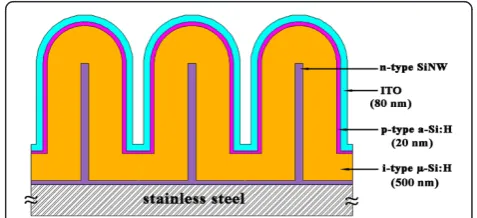
samples were transferred to a radio frequency magne-tron sputtering chamber for deposition of top ITO layer as front electrode. The sketch map of the SiNW-based μc-Si:H solar cell is shown in Figure 1.
Results and discussion
Morphology of n-type SiNWs and SiNW-basedμc-Si:H thin-film solar cells
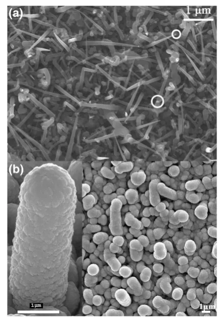
Figure 2a shows the scanning electron microscopy (SEM) image of as-grown n-type SiNWs. The SiNWs were synthesized for 20 min on the flexible stainless steel substrates. The bottom segment diameters of the SiNWs range from 50 to 200 nm, and their lengths ex-tend about 3μm. The white circles mark out the indium nanoparticles on top of the SiNWs. The growth mechan-ism of the SiNWs may be interpreted basically by means of the vapor–liquid-solid (VLS) mechanism. Figure 2b shows the as-obtained SiNW-based μc-Si solar cells. As we can see, the final p-type a-Si:H/i-type μc-Si:H/n-type SiNW structure diameter is about 1.5 μm and rather uniform along its length. Considering that the SiNW diameter is typically much smaller than the thickness of the i-type μc-Si:H covering layer, we can assume that a conformal and uniform coverage on top of the rough SiNW structures has been achieved.
Representation of acid treatment
Figure 3 presents the back-scattered electron SEM images of the n-type SiNWs before acid treatment (Figure 3a) and after acid treatment (Figure 3b). The white dots (marked by white arrows) denote the metal catalyst droplets for n-type SiNW VLS growth. As shown clearly, after acid treatment, the white dots are al-most absent. It means that the metal catalyst droplets on the tip of n-type SiNW have been removed.
[image:2.595.302.541.586.695.2] [image:2.595.56.293.641.725.2]The crystalline volume fraction of i-typeμc-Si:H layer Figure 4 shows the Raman spectra of i-type μc-Si:H of the cells. The Raman imaging microscope is equipped with a 514-nm wavelength line of an Ar laser. From the
Table 1 Synthesis conditions for the n-type silicon nanowires
Condition Value
SiH4+ PH3flow rate 6 sccm + 6 sccm
H2flow rate 60 sccm
Pressure 1.5 Torr
Substrate temperature 400°C
Radio frequency (13.56 MHz) power density 500 mW/cm2
SiH4gas is 100% pure, and PH3gas is 99 % H2diluted.
Raman spectra, the simple crystalline volume fraction (Xc) of the sample could be calculated as follows [19,20]:
Xc¼ðI520þI500Þ=ðI520þI500þI480Þ ð1Þ
where Ii is the area under the Gaussian centered at i, andI520+ I500+ I480is the total integrated intensity. The values of Xc evaluated from the deconvoluted spectra is about 28%.
Optical and electrical characterization
Figure 5 shows the optical reflectance spectrum of the cells over the full spectrum ranging from 400 to 1,100 nm. The black line and green line represent the spectra of the SiNW-basedμc-Si:H thin-film solar cells with acid treatment and without acid treatment, respectively. As can be seen, the optical reflectance of SiNW-based μc-Si:H thin-film solar cells is below 20% in the full spectrum and only about 10% in the range of 400- to
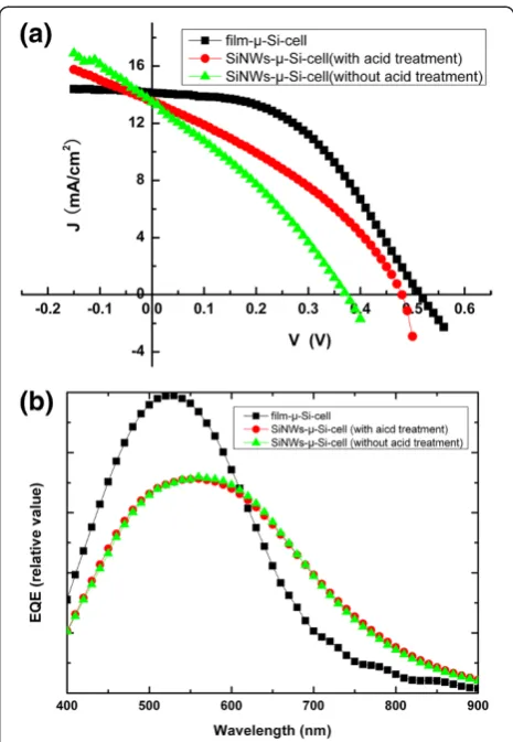
650-nm wavelengths. The average reflectance is approxi-mately 15%, which shows a 40% reduction compared to approximately 25% average reflectance of the corre-sponding planarμc-Si:H film solar cell (red line). It indi-cates that the low optical reflectance of the SiNW-based μc-Si:H thin-film solar cells is due to the light-trapping structure of SiNWs. Figure 6a shows the typical light current–voltage (I-V) curves of the cells measured under a solar simulator with air mass (AM) 1.5 (100 mA/cm2) illumination in the 0.07-cm2effective areas. The short-circuit current density (JSC), open-circuit voltage (VOC),
fill factor (FF), and conversion efficiency (η) derived from the I-V curve are listed in Table 2. The initial SiNW-based μc-Si:H thin-film solar cell has values of
VOC = 0.37 V, JSC = 13.36 mA/cm2, FF = 0.3, andη =
[image:3.595.307.538.88.433.2]1.48%. After acid treatment, the metal catalyst droplets have been removed from the top of the n-type SiNWs. The performance of the modified SiNW-based μc-Si:H thin-film solar cell has been improved remarkably with
Figure 2SEM images of (a) the n-type SiNWs and (b) the SiNW-basedμc-Si:H solar cells.The bottom segment diameters of the SiNWs range from 50 to 200 nm, and their lengths extend about 3
[image:3.595.59.287.91.416.2]μm. The white circles mark out the indium nanoparticles on top of the SiNWs. The final p-type a-Si:H/i-typeμc-Si:H/n-type SiNW structure diameter is about 1.5μm and rather uniform along its length.
the VOC = 0.48 V, JSC = 13.42 mA/cm2, FF = 0.35,
and η = 2.25%. It is worth mentioning that the VOC
improved by approximately 30% (from 0.37 to 0.48 V), and the JSC improved only by 0.4% (from 13.36 to
13.42 mA/cm2). Considering the influence of the metal catalyst droplets in the SiNW-based μc-Si:H thin-film solar cells, we think that the metal catalyst droplets in-crease the interface of the n-type SiNW and i-type μc-Si:H layer. Thus, the interface recombination would increase when the metal catalyst droplets exist. TheVOC
is most sensitive for interface recombination. So, it is most favorable for VOC improvement when the metal
[image:4.595.305.538.87.424.2]catalyst droplets were removed. In addition, refer to Figure 5, the metal catalyst droplets almost do not affect the optical reflectance of the cells. That could explain why the modified SiNW-based μc-Si:H thin-film solar
[image:4.595.57.290.88.262.2]Figure 5Optical reflectance spectrum of the cells.The optical reflectance spectrum of the cells over the full spectrum ranging from 400 to 1,100 nm. The black line and green line represent the spectra of the SiNW-basedμc-Si:H thin-film solar cells with acid treatment and without acid treatment, respectively. The red line represents the reflectance of the corresponding planarμc-Si:H film solar cell.
Figure 6I-Vand external quantum efficiency characteristics of the cells.(a) MeasuredI-Vcharacteristics of the SiNW-based solar cells (red dot line for cell with acid treatment and green triangle line for cell without acid treatment) and a corresponding planar silicon thin-film cell (black square line). (b) The external quantum efficiency of the SiNW-based solar cells and planar thin-film solar cell.
[image:4.595.57.290.488.654.2]Figure 4Raman spectra of i-typeμc-Si:H layer of the cells.The Raman spectra of i-typeμc-Si:H of the cells. The red line and line of black squares stand for the original measured data, and the green lines stand for the Gaussian fitting data. The Raman imaging microscope is equipped with a 514-nm wavelength line of an Ar laser.
Table 2 Parameters of the cells for light-soakingI-V characters
Parameters Cells
SiNWs cell (without acid
treatment)
SiNWs cell (acid treatment)
Planar film cell
Voc(V) 0.37 0.48 0.51
Jsc(mA/cm2) 13.36 13.42 14
FF 0.3 0.35 0.46
η(%) 1.48 2.25 3.28
Measured under solar simulator with AM 1.5 (100 mA/cm2
[image:4.595.305.539.614.716.2]cell has little improvement in JSC. The current–voltage
curve of the corresponding planarμc-Si:H film solar cell is also shown in Figure 6a (black solid square line) for contrast. As can be seen, the performance of the SiNW-based cells is not as good as that of the corresponding planar film cell, especially in terms of VOCand FF. The
[image:5.595.305.540.325.738.2]unsatisfactory performance of the SiNW-based cell could be attributed to more interface recombination which brings higher leakage current and lower shunt resistance [21]. Thus, the interface passivation is the most import-ant for SiNW-based thin-film solar cells.
Figure 6b shows the external quantum efficiency (EQE) of the SiNW-based μc-Si:H solar cells (red dot line for cells with acid treatment and green triangle line for cells without acid treatment) and planarμc-Si:H film solar cell (black square line). From the picture, the EQE of the SiNW-based cells has a definite improvement in the wavelength range of 630 to 900 nm that is due to the light-trapping effect of SiNWs. However, in the short wavelengths (from 400 to 630 nm), the SiNW-based cells show lower EQE than the corresponding planar film cell, which is inconsistent with the results of the op-tical reflectance spectrum shown in Figure 5. It may be explained as follows: first, the anti-reflection effect of SiNW-based cells in short wavelengths is not as good as in long wavelengths (refer to Figure 5); second, the inter-face of the n-type SiNWs and i-typeμc-Si:H layer influ-ences the collection of photo-induced electrons, especially the photo-induced electrons in the short-wavelength range.
Conclusions
We have produced a radial n-i-p structure SiNW-based μc-Si:H thin-film solar cell on stainless steel foil by plasma-enhanced chemical vapor deposition. The SiNW solar cell displays a very low optical reflectance over a broad range of wavelengths (400 to 1,100 nm) due to its natural anti-reflective structure. The modified open-circuit voltage, short-open-circuit current density, and conver-sion efficiency under AM 1.5 illumination were 0.48 V, 13.42 mA/cm2, and 2.25%, respectively. The EQE mea-surements show that the EQE response of SiNW solar cells is improved greatly in the wavelength range of 630 to 900 nm compared to the corresponding planar film solar cells. Further, we will focus on improving the SiNW solar cells by minimizing shunts, reducing contact resistance, and improving the open-circuit voltage.
Abbreviations
EQE: external quantum efficiency; FF: fill factor; ITO: indium tin oxide; Jsc: short-circuit current density; PECVD: plasma-enhanced chemical vapor deposition; SEM: scanning electron microscope; SiNW: silicon nanowire; VLS: vapor–liquid–solid;Voc: open-circuit voltage;μc-Si:H: Hydrogenated microcrystalline silicon.
Competing interests
The authors declare that they have no competing interests.
Authors’contributions
XBZ and QW conceived of the study, participated in its design and coordination, and revised the manuscript. XX participated in its design and coordination, drafted the manuscript, and carried out the experiments on fabrication of SiNWs. PY carried out the measurement and analysis of optical and electoral characterization. HL carried out the measurement and analysis of the Raman spectrum. JL and XDZ carried out the PECVD experiments for silicon thin-film deposition. All authors read and approved the final manuscript.
Acknowledgments
This work was financially supported by the National High Technology Research and Development Program (863 Program) of China (no. 2011AA050504), the Knowledge Innovation Program of the Chinese Academy of Sciences (no. 1KGCX2-YW-383-1) and the Key Laboratory of Nanodevices and Applications, Suzhou Institute of Tech and Nano-Bionics, Chinese Academy of Sciences (no. 12JG01).
Received: 3 October 2012 Accepted: 30 October 2012 Published: 12 November 2012
References
1. Lewis NS:Toward cost-effective solar energy use.Science2007,
315:798–801.
2. Shah AV, Schade H, Vanecek M, Meier J, Vallat-Sauvain E, Wyrsch N, Kroll U, Droz C, Bailat J:Thin-film silicon solar cell technology.Prog Photovoltaics 2004,12:113–142.
3. Tian BZ, Zheng XL, Kempa TJ, Fang Y, Yu NF, Yu GH, Huang JL, Lieber CM:
Coaxial silicon nanowires as solar cells and nanoelectronic power sources.Nature2007,449:885–890.
4. Kayes BM, Atwater HA, Lewis NS:Comparison of the device physics principles of planar and radial p-n junction nanorod solar cells.J Appl Phys2005,97:1140302–1140311.
5. Jie Tang JS, Lili Z, Zhongquan M:Fabrication and optical properties of silicon nanowires arrays by electroless Ag-catalyzed etching.Nano-Micro Lett2011,3:129–134.
6. Huang YF, Chattopadhyay S, Jen YJ, Peng CY, Liu TA, Hsu YK, Pan CL, Lo HC, Hsu CH, Chang YH, Lee CS, Chen KH, Chen LC:Improved broadband and quasi-omnidirectional anti-reflection properties with biomimetic silicon nanostructures.Nat Nanotechnol2007,2:770–774.
7. Hu L, Chen G:Analysis of optical absorption in silicon nanowire arrays for photovoltaic applications.Nano Lett2007,7:3249–3252.
8. Street RA, Qi P, Lujan R, Wong WS:Reflectivity of disordered silicon nanowires.Appl Phys Lett2008,93(163109):3.
9. Garnett E, Yang PD:Light trapping in silicon nanowire solar cells.Nano Lett2010,10:1082–1087.
10. Li XC, Li JS, Chen T, Tay BK, Wang JX, Yu HY:Periodically aligned Si nanopillar arrays as efficient antireflection layers for solar cell applications.Nanoscale Res Lett2010,5:1721–1726.
11. Yuriy Vashpanov J-IJ:Optical absorption and photoelectron collection properties of silicon wafers with conical quantum nanocrystals structure.
Nano-Micro Lett2010,2:149–153.
12. Pei ZW, Chang ST, Liu CW, Chen YC:Numerical simulation on the photovoltaic behavior of an amorphous-silicon nanowire-array solar cell.
IEEE Electr Device L2009,30:1305–1307.
13. Yu LW, O’Donnell B, Alet PJ, Cabarrocas PRI:All-in-situfabrication and characterization of silicon nanowires on TCO/glass substrates for photovoltaic application.Sol Energ Mat Sol C2010,94:1855–1859. 14. Jinyoun C, O’Donnell B, Yu LW, Kim K-H, Ngo I, Cabarrocas PR:Sn-catalyzed
silicon nanowire solar cells with 4.9% efficiency grown on glass.
Photovolt: Res Appl2012, doi:10.1002/pip.1245.
15. Yu LW, Fortuna F, O’Donnell B, Jeon T, Foldyna M, Picardi C:Cabarrocas PRi: bismuth-catalyzed and doped silicon nanowires for one-pump-down fabrication of radial junction solar cells.Nano Lett2012,
12:4153–4158.
17. Jeon MS, Tomitsuka Y, Aoyagi M, Kamisako K:Effects of hydrogen radical treatment on fabrication of catalyst nanoparticles from metal oxide film at low temperature and synthesis of silicon nanowires.Jpn J Appl Phys 2009,48(015002):1–4.
18. Xie XB, Zeng XB, Yang P, Wang C, Wang QM:In situformation of indium catalysts to synthesize crystalline silicon nanowires on flexible stainless steel substrates by PECVD.J Cryst Growth2012,347:7–10.
19. Wang Q, Yue GZ, Li J, Han DX:A combinatorial study of materials in transition from amorphous to microcrystalline silicon.Solid State Commun1999,113:175–178.
20. Veprek S, Sarott FA, Iqbal Z:Effect of grain-boundaries on the Raman-spectra, optical-absorption, and elastic light-scattering in nanometer-sized crystalline silicon.Phys Rev B1987,36:3344–3350. 21. Tang M, Chang ST, Chen TC, Pei ZW, Wang WC, Huang J:Simulation of
nanorod structures for an amorphous silicon-based solar cell.Thin Solid Films2010,518:S259–S261.
doi:10.1186/1556-276X-7-621
Cite this article as:Xieet al.:Radial n-i-p structure SiNW-based microcrystalline silicon thin-film solar cells on flexible stainless steel.
Nanoscale Research Letters20127:621.
Submit your manuscript to a
journal and benefi t from:
7 Convenient online submission 7 Rigorous peer review
7 Immediate publication on acceptance 7 Open access: articles freely available online 7 High visibility within the fi eld
7 Retaining the copyright to your article