S P E C I A L I S S U E A R T I C L E
Influence of Ni Catalyst Layer and TiN Diffusion Barrier
on Carbon Nanotube Growth Rate
Jean-Baptiste A. Kpetsu•Pawel Jedrzejowski •Claude Coˆte´• Andranik Sarkissian•Philippe Me´rel•Philips Laou •
Suzanne Paradis•Sylvain De´silets• Hao Liu•Xueliang Sun
Received: 11 August 2009 / Accepted: 16 January 2010 / Published online: 4 February 2010
ÓThe Author(s) 2010. This article is published with open access at Springerlink.com
Abstract Dense, vertically aligned multiwall carbon nanotubes were synthesized on TiN electrode layers for infrared sensing applications. Microwave plasma-enhanced chemical vapor deposition and Ni catalyst were used for the nanotubes synthesis. The resultant nanotubes were charac-terized by SEM, AFM, and TEM. Since the length of the nanotubes influences sensor characteristics, we study in details the effects of changing Ni and TiN thickness on the physical properties of the nanotubes. In this paper, we report the observation of a threshold Ni thickness of about 4 nm, when the average CNT growth rate switches from an increasing to a decreasing function of increasing Ni thick-ness, for a process temperature of 700°C. This behavior is likely related to a transition in the growth mode from a predominantly ‘‘base growth’’ to that of a ‘‘tip growth.’’ For Ni layer greater than 9 nm the growth rate, as well as the CNT diameter, variations become insignificant. We have also observed that a TiN barrier layer appears to favor the growth of thinner CNTs compared to a SiO2layer.
Keywords Carbon nanotubesPlasma-enhanced chemical vapor depositionNi catalyst
TiN diffusion barrierScanning electron microscopy
Introduction
Due to their known or potentially interesting electronic, mechanical, thermal, and optical properties, carbon nano-tubes (CNTs) are being investigated in a wide range of fields for scientific or industrial applications [1]. Opto-electronic properties of nanotubes, and in particular tun-ability of their spectral response over a wide range of wavelength from about 1 to about 10lm (i.e., from about 1 eV to below 100 meV), make them very interesting component for infrared sensors [2–4]. Our study aims at investigating the properties of vertically aligned CNTs synthesized on Ni/TiN/Si substrates using microwave plasma-enhanced chemical vapor deposition (MPECVD) technique for further applications in infrared imaging devices.
Despite a great amount of progress and breakthroughs that have been made toward synthesis and characterization of these versatile nanostructures built from sp2carbon units [5–8], several questions regarding controlled synthesis processes remain unanswered, including the role of sub-strate morphology in CNT growth process [9–11]. It is still a challenge to develop processes that produce CNTs with predetermined and homogeneous basic structural parame-ters such as their length, diameter, and surface distribution [12–14]. Despite recent modeling efforts [15–17], those structural parameters still are difficult to fully control during the synthesis. A detailed understanding of the growth process is necessary since the length, diameter, and density of the CNTs influence the characteristics of potential sensors.
In this paper, we focus on studying the effects of the thickness of Ni catalyst layer and its underlying TiN electrode layer on the growth rate and properties of CNTs.
J.-B. A. Kpetsu (&)P. JedrzejowskiC. Coˆte´A. Sarkissian Plasmionique Inc., 1650 boul. Lionel Boulet, Varennes, QC J3X 1S2, Canada
e-mail: [email protected]
P. Me´relP. LaouS. ParadisS. De´silets
Defence Research & Development Canada—Valcartier, 2459 boul. Pie XI Nord, Val-Belair,
QC G3J 1X5, Canada
H. LiuX. Sun
Experimental Details
We have used prime grade N-type Sb doped Si substrates with\100[orientation in these experiments. The TiN interlayer has a dual functionality in our sensor structure. It acts as an electrode that provides the electrical contact for the CNTs, and it also forms a protective barrier layer against diffusion of the Ni catalyst and formation of NiSix. This silicide formation occurs at temperatures above 300°C [18]. The TiN layer was deposited by DC-magnetron sputtering. A 99.5% pure TiN target was used, and the Si substrates were heated to 500°C for the deposition in a reactive Nitrogen atmosphere at 1.2 mTorr. TiN thickness of 100 nm was used in our experiments. The Ni catalyst layer was then deposited by RF-magnetron sputtering using a 99.9% pure Ni target at ambient temperature under Ar atmosphere at 0.72 mTorr. After deposition of TiN and Ni layers, the resulting Ni/TiN/Si material was then trans-ferred in air into the MPECVD reactor.
The 2.45-GHz microwave generator of the MPECVD system could be operated with the power up to 1.0 kW. The H2, CH4, and Ar process gases were introduced independently into the chamber through electronically controlled mass flow controllers. The substrates could be heated up to over 800°C and maintained at controlled constant temperature using a PID.
We used a synthesis procedure that included a H2 plasma pretreatment step. The pretreatment reduces NiOx and then activates the catalyst for the subsequent growth process [19]. To assure process reproducibility, the cham-ber was pumped to 10-6Torr prior to introducing the H2 gas. The substrates were gradually heated to the growth temperature of 700°C in about 30 min. The temperature was kept constant for another 10 min, before the ignition of the H2plasma at 4 Torr and 900 W of microwave power. After 10 min of H2plasma pretreatment, the CH4gas was then introduced into the chamber for the CNT synthesis at 900 W. The total pressure in the chamber was maintained at 5 Torr during the 20-min growth process, for most of our experiment reported here. Our experiments had established an optimized CH4:H2 ratio of 1:4. Ar refilling of the chamber was used at the end of the growth process to cool the samples down to ambient temperature. It should be noted that the substrate temperature could have increased during experiment, as a result of contact with plasma. However, these variations were identical for all samples.
Various complementary characterization tools were used to study the entire synthesis process. A Dektak pro-filometer was used for TiN thicknesses evaluation and ellipsometry for the thinner Ni films. Scanning electron microscopy (SEM), transmission electron microscopy (TEM), and atomic force microscopy (AFM) were used to investigate structural features of CNTs such as length or
diameter distribution and substrate morphology, including Ni cluster size at various steps of the process.
Results and Discussion
The SEM observations reveal that the Ni catalyst films and the TiN buffer layer deposited at ambient temperature were found to be smooth and homogenous. However, as shown in Fig. 1, the structure of*2 to*22 nm thick as-depos-ited Ni film is altered by the fragmentation and reorgani-zation of the Ni particles during the substrate heating and H2 plasma pretreatment stage, prior to the CNT growth process.
The first column of Fig. 1(images (a) to (i)) shows the SEM images of those Ni layers with various thicknesses after the pretreatment process. SEM images in the second column of Fig. 1 show the surface structure of samples identical to those in the first column, after 2 min of CNT synthesis process at 5 Torr and 900 W microwave power, following the pretreatment step. The third column of Fig.1
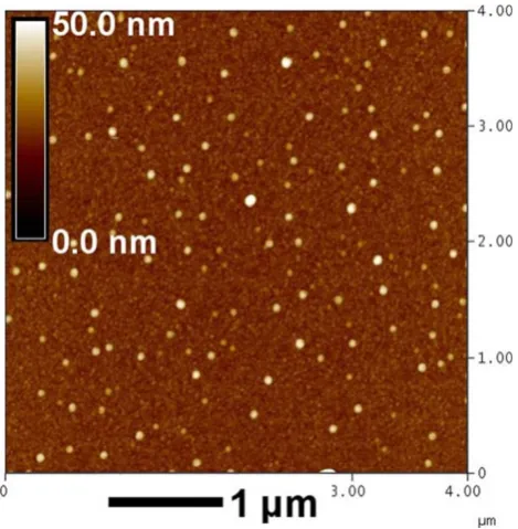
shows images of CNTs grown after 20 min of processing time, under similar operating conditions as in the second column. For Ni films thicker than *4 nm, the effect of pretreatment on the catalyst is clearly seen in the first and second columns, as agglomeration and granular structures of the surface formed by a fragmentation and reorganiza-tion of the deposited smooth Ni layer. AFM analysis, shown in Fig. 2, indicates that the films with *2 to
*4 nm thick Ni catalyst also have granular structures after pretreatment, although they appear smooth and homoge-nous in the SEM images.
The particle size estimated from AFM and SEM images, assuming spherical particles, is plotted in Fig. 3. This assumption appears reasonable as it conforms to what is expected from the conservation of mass of the deposited film. For example, using these assumptions and the mea-sured number density of particles, the expected diameter for *9-nm-thick film should be *73 nm, for * 13-nm-thick film should be about 106 nm, and for*22-nm-thick film should be about 142 nm. These numbers are in good agreement with the estimated particle sizes shown in Fig.3.
The observed increase in average size of the Ni clusters with the sputtered Ni thickness is similar to result reported by different groups [18,20]. However, in our experiments, using Si substrates with a polycrystalline TiN barrier layer, a substantially smaller average cluster size was observed compared to those reported in reference [18], where Si substrates with a SiO2 barrier layer were used (e.g.,
Fig. 1 SEM photographs of samples with a constant TiN thickness of 100 nm and varying Ni thickness (first column) after the H2plasma
[image:3.595.268.547.53.698.2]surface morphology and ion to neutral flux ratio during the magnetron sputter deposition process, which influences the film structure, and also during the heating process follow-ing the film deposition [21]. In our case, the morphological factors are believed to be the reason for difference in cluster size. The standard deviation of the cluster size is also plotted as error bars in Fig.3. Homogeneity of the cluster size distribution is much better for the case of the thinner layers. For example, a distribution range was observed to change from*20 nm to more than 200 nm as Ni thicknesses changes from *4 to *22 nm, which
implies that small Ni thicknesses are also to be preferred, if more homogeneous cluster size distribution is needed during the synthesis of carbon nanotubes.
Figure4shows the evolution of the average CNT length and consequently the average growth rate as the thickness of Ni catalyst layer increases. We can distinguish three zones in the figure. In the first zone, for the Ni thickness up to*4 nm, the CNT length increases up to almost 18lm. The second zone extends beyond the optimum thickness that occurs at about 4 nm of Ni, the CNT thickness decreases down to*6lm for Ni thickness up to*9 nm. In a third zone, for higher Ni thicknesses, the CNT length stabilizes at*6lm.
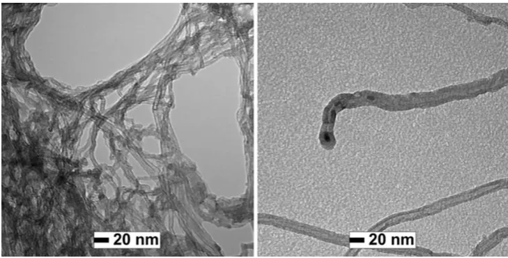
The presence of a maximum CNT length at * 4-nm-thick Ni catalyst layer is possibly related to a change in the preferential CNT growth mode. The SEM images, com-bined with limited number of TEM images available for some of our samples (see Fig. 5), do not contradict this possibility. The process of ‘‘tip growth’’ versus ‘‘base growth’’ depends on the interactions between the catalyst film and the substrate. If the interaction is strong between the two layers, then ‘‘base growth’’ is the dominant mechanism, otherwise ‘‘tip growth’’, where the catalytic particles are lifted on top of the growing CNTs, takes place [22].
The tendency of average CNT diameter to increase as a result of the increasing cluster size when the Ni thickness is increased could be seen in Fig. 6. It is to be noted that the impact of synthesis temperature on growth mechanism has been reported previously [23]. However, in our experi-ments, the temperature was an invariable and the observed change in diameter of the CNT with Ni catalyst thickness appears to be related to the cluster size increase.
The trend of the decreasing average CNT length with the increase in catalyst thickness above 4 nm (seen in
Fig. 4 Initial Ni film thickness influence on final CNT length measured by SEM. Relative error on length data is less than 2%
Fig. 2 AFM image of a 3.9-nm Ni film on a 100-nm TiN electrode after the pretreatment. The sample is the same as in image (d) of Fig.1
[image:4.595.54.289.57.297.2] [image:4.595.53.287.355.525.2] [image:4.595.307.541.513.686.2]Fig.4) was also reported by other authors for Ni [18] and Co [20] catalysts. However, in those reports, authors did not observe any ‘‘tip growth’’ mode, very likely, due to differences in the interactions between the catalysts and the substrates, stemming from differences in selected substrate and catalyst materials. The decrease in CNT length can be attributed to the increased diameter of CNTs (Fig.6) for the same flux of carbon atoms. Furthermore, as the diam-eter of nanotubes becomes larger, the heat transfer to the catalyst could also be reduced as the ratio of CNT tubes surface to the volume of catalyst decreases, which in turn could result in termination of the growth process. Decay of catalyst activity by products of gas-phase carbon pyrolysis has also been suggested to explain the growth termination, but the precise mechanism has not been identified [24].
In the ‘‘third zone’’, no apparent change in growth rate is seen with increasing the thickness of the Ni catalyst layer
to up to 22 nm. The observed stabilization of the average CNT length at *6 nm is linked to a stabilization of the average CNT diameter at *27 nm (Fig.6) even if the cluster size still increases with increasing Ni thickness throughout this zone. The observed invariance of the CNT diameter size with catalyst cluster size increase is not well understood. Some models suggest that the diameter and structure of single wall carbon nanotubes (SWCNTs) are linked to the scale size of Be´nard–Marangoni type insta-bilities that are triggered in the liquid catalyst [25]. How-ever, for temperature gradient-driven instabilities, the turbulence scale length could be independent of the catalyst droplet size, which could be one likely explanation for the observed constant CNT diameter, even if the CNTs grown in our experiments are multiwall carbon nanotubes (MWCNTs) as seen in Fig.5.
Conclusions
MPECVD was used to grow vertically aligned, dense multiwall carbon nanotubes on TiN electrodes deposited on Si substrates with the use of Ni catalyst. The morphology of the nanotubes and their physical characteristics (length and distribution) were studied for future applications in infrared photodetectors. We have observed an initial rapid increase in the average CNT growth rate to a maximum of
*14 nm s-1 for Ni thickness increasing from *2 to
*4 nm, followed by a gradual decrease in the growth rate, when the Ni catalyst thickness is increased from *4 to
*9 nm. The growth rate appears to saturate for thicker Ni layers. It appears that this change in growth rate at the observed threshold Ni thickness could be linked to a change in the preferential growth mode of the CNTs, from ‘‘base growth’’ to ‘‘tip growth.’’ Such a transition occurring Fig. 5 TEM images of CNTs grown at 5 Torr on the 2.7-nm (on left) and 4.7-nm (on right) thick Ni films
[image:5.595.114.479.57.242.2] [image:5.595.53.289.277.449.2]with varying catalyst thickness at the same CNT growth temperature should be considered in ongoing CNT growth modeling efforts. We have also observed that the Ni thickness below 4 nm is preferable for more homogenous Ni cluster size distribution and consequently CNT diameter distribution. Also, the polycrystalline TiN interlayer appears to favor thinner nanotubes in comparison with SiO2buffer layer reported by other groups. The influence of the underlying TiN electrode on the nanotube growth process and the impact of the physical CNT features on spectral sensitivity are subject of our current and future studies.
Acknowledgments This work was supported by the Department of National Defense (DND). The authors wish to thank Louis Durand, David Alain and Nicole Gagnon (technical support), Andrew Achkar (AFM), and Barry Stansfield for useful discussions.
Open Access This article is distributed under the terms of the Creative Commons Attribution Noncommercial License which per-mits any noncommercial use, distribution, and reproduction in any medium, provided the original author(s) and source are credited.
References
1. M. Paradise, T. Goswani, Mater. Des.28, 1477–1489 (2007) 2. J.M. Xu, Infr. Phys. Tech.42, 485–491 (2001)
3. J.W.G. Wildoer, L.C. Venema, A.G. Rinzler, R.E. Smally, C. Dekker, Nature391, 59–62 (1998)
4. T.W. Odom, J. Huang, P. Kim, C.M. Lieber, Nature391, 62–64 (1998)
5. J. Wu, M. Eastman, T. Gutu, M. Wyse, J. Jiao, S.-M. Kim, M. Mann, Y. Zhang, K.B.K. Teo, Appl. Phys. Lett.91(173122), 1–3 (2007)
6. M. Tarasov, J. Svensson, L. Kuzmin, E.E.B. Campbell, Appl. Phys. Lett.90(163503), 1–3 (2007)
7. A.A. Puretzky, G. Eres, C.M. Rouleau, I.N. Ivanov, D.B. Geo-hegan, Nanotechnology19(055605), 1–5 (2008)
8. M. Jo¨nsson, O.A. Nerushev, E.E.B. Campbell, Nanotechnology
18(305702), 1–5 (2007)
9. H. Liu, Y. Zhang, D. Arato, R. Li, P. Me´rel, X. Sun, Surf. Coat. Technol.202, 4114–4120 (2008)
10. T.D. Arcos, M.G. Garnier, J.W. Seo, P. Oelhafen, V. Thommen, D. Mathys, J. Phys. Chem. B108, 7728–7734 (2004)
11. P.M. Parthangal, R.E. Cavicchi, M.R. Zachariah, Nanotechnol-ogy18(185605), 1–5 (2007)
12. P. Wang, J. Lu, O. Zhou, Nanotechnology 19(185605), 1–7 (2008)
13. H. Amara, C. Bichara, F. Ducastelle, Phys. Rev. Lett. 100
(056105), 1–4 (2008)
14. N. Grobert, Mater. Today10(1–2), 28–35 (2007)
15. A.C. Lysaght, W. Chiu, Nanotechnology19(165607), 1–8 (2008) 16. S. Naha, I.K. Puri, J. Phys. D Appl. Phys.41(065304), 1–6 (2008) 17. R.F. Wood, S. Pannala, J.C. Wells, A.A. Puretzky, D.B.
Geohe-gan, Phys. Rev. B75(235446), 1–8 (2007)
18. M. Chhowalla, K.B.K. Teo, C. Ducati, N.L. Rupesinghe, G.A.J. Amaratunga, A.C. Ferrari, D. Roy, J. Robertson, W.I. Milne, J. Appl. Phys.90(10), 5308–5317 (2001)
19. J.H. Yen, I.C. Leu, C.C. Lin, M.H. Hon, Diam. Relat. Mater.13, 1237–1241 (2004)
20. C. Bower, O. Zhou, W. Zhu, D.J. Werder, S. Jin, Appl. Phys. Lett.77(17), 2767–2769 (2000)
21. M. Meyyappan, L. Delzeit, A. Cassel, D. Hash, Plasma Sources Sci. Technol.12, 205–216 (2003)
22. V.I. Merkulov, A.V. Melechko, M.A. Guillorn, D.H. Lowndess, M.L. Simpson, Appl. Phys. Lett.79(18), 2970–2972 (2001) 23. S. Esconjauregui, C.M. Whelan, K. Maex, Nanotechnology
18(015602), 1–11 (2007)
24. E.R. Meshot, A.J. Hart, Appl. Phys. Lett.92(113107), 1–3 (2008) 25. F. Larouche, O. Smiljanic, X. Sun, B. Stansfield, Carbon43, 986–