N A N O E X P R E S S
Open Access
Efficient spin filter using multi-terminal quantum
dot with spin-orbit interaction
Tomohiro Yokoyama
*and Mikio Eto
Abstract
We propose a multi-terminal spin filter using a quantum dot with spin-orbit interaction. First, we formulate the spin Hall effect (SHE) in a quantum dot connected to three leads. We show that the SHE is significantly enhanced by the resonant tunneling if the level spacing in the quantum dot is smaller than the level broadening. We stress that the SHE is tunable by changing the tunnel coupling to the third lead. Next, we perform a numerical
simulation for a multi-terminal spin filter using a quantum dot fabricated on semiconductor heterostructures. The spin filter shows an efficiency of more than 50% when the conditions for the enhanced SHE are satisfied. PACS numbers: 72.25.Dc,71.70.Ej,73.63.Kv,85.75.-d
Introduction
The injection and manipulation of electron spins in semiconductors are important issues for spin-based elec-tronics,“spintronics.”[1] The spin-orbit (SO) interaction can be a key ingredient for both of them. The SO inter-action for conduction electrons in direct-gap semicon-ductors is written as
HSO= λ
¯ hσ·
p×∇U(r), (1)
where U(r) is an external potential, ands indicates the electron spin s =s/2. The coupling constant l is largely enhanced in narrow-gap semiconductors such as InAs, compared with the value in the vacuum [2].
In two-dimensional electron gas (2DEG;xyplane) in
semiconductor heterostructures, an electric field perpen-dicular to the 2DEG,U(r) =eEz, induces the Rashba SO interaction [3,4]
HSO= α
¯
h(pyσx−pxσy), (2)
where α=eEλ. The Rashba SO interaction can be
tuned by the external electric field, or the gate voltage [5-7]. In the spin transistor proposed by Datta and Das [8], electron spins are injected into the 2DEG from a ferromagnet, and manipulated by tuning the strength of Rashba SO interaction. However, the spin injection from
a ferromagnetic metal to semiconductors is generally not efficient, less than 0.1%, because of the conductivity mismatch [9]. To overcome this difficulty, the SO inter-action may be useful for the spin injection into semicon-ductor without ferromagnets. Several spin filters were proposed utilizing the SO interaction, e.g., three-term-inal devices based on the spin Hall effect (SHE) [10-12], a triple-barrier tunnel diode [13], a quantum point con-tact [14,15], and an open quantum dot [16-19].
The SHE is one of the phenomena utilized to create a spin current in the presence of SO interaction. There are two types of SHE. One is an intrinsic SHE which creates a dissipationless spin current in the perfect crys-tal [20-22]. The other is an extrinsic SHE caused by the spin-dependent scattering of electrons by impurities [23-25]. In our previous articles [26-28], we have formu-lated the extrinsic SHE in semiconductor heterostruc-tures with an artificial potential created by antidot, scanning tunnel microscope (STM) tip, etc. The artificial potential is electrically tunable and may be attractive as well as repulsive. We showed that the SHE is signifi-cantly enhanced by the resonant scattering when the attractive potential is properly tuned. We proposed a multi-terminal spin filter including the artificial poten-tial, which shows an efficiency of more than 50% [27].
In the present article, we investigate an enhancement of the SHE by the resonant tunneling through a quan-tum dot (QD) with strong SO interaction, e.g., InAs QD [29-34]. The QD shows a peak structure of the current as a function of gate voltage, the so-called Coulomb * Correspondence: [email protected]
Faculty of Science and Technology, Keio University, 3-14-1 Hiyoshi, Kohoku-ku, Yokohama 223-8522, Japan
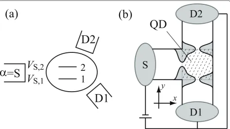
oscillation. At the current peaks, the resonant tunneling takes place at low temperatures. First, we consider an impurity Anderson model with three leads, as shown in Figure 1a. There are two energy levels in the QD. We show a remarkable enhancement of the SHE when the level spacing in the QD is smaller than the level broad-ening. The SHE is electrically tunable by changing the tunnel coupling to the third lead.
Next, we perform a numerical simulation for a spin-filtering device fabricated on semiconductor heterostruc-tures, in which a QD is connected to three leads (Figure 1b). The device is described using the tight-binding model of square lattice, which discretizes the two-dimensional space [35]. We find that the spin filter indi-cates an efficiency of more than 50% when some condi-tions are satisfied.
Formulation of spin Hall effect
To formulate the SHE in a multi-terminal QD, we begin with an impurity Anderson model shown in Figure 1a.
The number of leads is denoted by N (N ≥ 2). As a
minimal model, we consider two energy levels in the QD; ε1, and ε2. We assume that the wavefunctions,ψ1
andψ2, in the QD are real in the absence of a magnetic
field. Since the SO interaction (1) includes the
momentump = -iħ∇, which is a pure imaginary
opera-tor, the diagonal elements of the SO interaction,〈j|HSO|
j〉 (j = 1, 2), disappear. The off-diagonal elements are denoted by
2|HSO|1=±iSO
2
for spin ±1/2 in the direction of〈2|(p×∇U)|1〉. The state |j〉in the QD is connected to leadaby tun-nel coupling,Va,j(j = 1, 2). The strength of the tunnel coupling is characterized by the level broadening,Γa=
πνa(Va,12 +Va,22), whereνais the density of states in
the lead. The leads have a single channel of conduction electrons. Unpolarized electrons are injected into the QD from source lead (a= S) and output to drain leads (Dn;n= 1, 2, ...,N- 1). The electric voltage is identical in the (N- 1) drain leads. The current to the drain Dn of each spin component,In,±, is generally formulated in
terms of Green functions in the QD [36].
We formulate the SHE in the vicinity of the Coulomb peaks where the resonant tunneling takes place. Neglecting the electron-electron interaction, we obtain an analytic expression of the conductance Gn,±for spin
±1/2 [37]. We find that the SHE is absent (G1,+= G1,-)
when the number of leads is N= 2, as pointed out by
(a)
(b)
D1
α=S
V
S
,1
V
S
,2
1
2
QD
x
y
D2
S
[image:2.595.64.538.406.672.2]D1
D2
Figure 1Models of a multi-terminal spin filter using a quantum dot with SO interaction.(a)Impurity Anderson model with three leads. There are two energy levels (j= 1, 2) in the quantum dot. They are connected to lead by tunnel coupling,Va,j(b)A three-terminal spin-filtering
other groups (see Ref. [18] and related references cited therein). ForN= 3, the conductance to lead D1 is given by
G1,±=e 2
h 4SD1
|D|2
(εF−ε1)eD1,2eS,2+ (εF−ε2)eD1,1eS,1 2
+
±SO
2 (eS×eD1)3+D2(eD1×eD2)3(eS×eD2)3 2
. (3)
Here,Dis the determinant of the QD Green function, which is independent of spin ±1/2 (see Ref. [37] for detail). We introduce unit vectors, ea(a = S, D1, and
D2), whereeα,j=Vα,j/ (Vα,1)2+ (Vα,2)2, in the
pseudo-spin space representing levels 1 and 2 in the QD. (a×
b)3=a1b2 -a2b1.
In Equation 3, the spin current [∝(Gn,+-Gn,-)] stems
from the interplay between SO interaction, ΔSO, and
tunnel coupling to lead D2, ΓD2. We exclude specific
situations in which two fromeS,eD1, andeD2are parallel
to each other hereafter. We find the conditions for a large spin current as follows: (i) The level spacing, Δε=
ε2 -ε1, is smaller than the level broadening by the
tun-nel coupling to leads S and D1, ΓS+ΓD1. (ii) The Fermi
level in the leads is close to the energy levels in the QD (resonant condition). (iii) The level broadening by the tunnel coupling to lead D2,ΓD2, is comparable with the
[image:3.595.62.537.323.680.2]strength of SO interactionΔSO.
Figure 2 shows the conductance of each spin, G1,+
(solid line) andG1,- (broken line), as a function ofεd= (ε1+ε2)/2, in the case of N = 3. The conductance shows
a peak reflecting the resonant tunneling around the Fermi level in the leads, which is set to be zero. We set
ΓS= ΓD1≡ Γ, whereas (a) ΓD2 = 0.2Γ, (b) 0.5Γ, (c) Γ,
and (d) 2Γ. The level spacing in the QD is Δε = 0.2Γ. The strength of SO interaction isΔSO = 0.2Γ. The
cal-culated results clearly indicate that the SHE is enhanced by the resonant tunneling around the peak. We obtain a
-4
ε
d
/
Γ
4
0
G
1,
+ −
(
e
2
/
h
)
0.2
0
0.1
0
0.1
0
0.1
0
0.1
(a)
(b)
(c)
(d)
Figure 2Calculated results of the conductanceG1,±to the drain 1 for spin ±1/2 in the impurity Anderson model with three leads. In
the abscissa,εd= (ε1+ε2)/2, whereε1andε2are the energy levels in the quantum dot. Solid and broken lines indicateG1,+andG1,-,
respectively. The level broadening by the tunnel coupling to the source and drain 1 isΓS=ΓD1≡Γ(VS,1/VS,2= 1/2,VD1,1/VD1,2= -3), whereas
large spin current whenΓD2~ΔSO, as pointed out
pre-viously. Therefore, the SHE is tunable by changing the tunnel coupling to the third lead,ΓD2.
Numerical simulation
To confirm the enhancement of SHE discussed using a simple model, we perform a numerical simulation for a spin-filtering device in which a QD is connected to
three leads, as shown in Figure 1b. 2DEG in the xy
plane is formed in a semiconductor heterostructure. Reservoir S is a source from which spin-unpolarized electrons are injected into the QD. The voltage is identi-cal in reservoirs D1 and D2.
Model
A QD is connected to reservoirs through quantum wires
of width W. A hard-wall potential is assumed at the
edges of the quantum wires. The QD is formed by quantum point contacts on the wires. The potential in a quantum wire along thexdirection is given by [38]
U(x,y,U0) =
U0
2
1 + cos
2πx L
+EF ±
y−y±(x)
2
θ(y2−y±(x)2)
×θ(x+L)θ(L−x),
(4)
with
y±(x) =±W 4
1−cos
2πx L
. (5)
where θ(t) is a step function [θ= 1 for t> 0, andθ= 0 for t < 0], U0 is the potential height of the saddle
point. The parameter Δcharacterizes the confinement
in the y direction, whereas L is the thickness of the
potential barrier. When the electrostatic energy in the QD is changed by the gate voltage Vg, the potential is
modified to U(x,y,U0 -eVg)+eVg inside the QD region
[netted square region in Figure 1b] and U(x, y, U0)
out-side of the QD region (The potential in the three quan-tum wires is overlapped by each other inside the QD region. Thus, we cut off the potential at the diagonal lines in the netted square region in Figure 1b).
The gradient of Ugives rise to the SO interaction in Equation 1, as
HSO= λ
¯ hσz
px∂U ∂y −py
∂U ∂x
. (6)
Although the SO interaction is also created by the hard-wall potential at the edges of the leads, it is negligi-ble because of a small amplitude of the wavefunction there [27].
The device is described using the tight-binding model of square lattice, which discretizes the real space in two dimensions [35,38]. The width of the leads is W= 30a,
with lattice constant a. The effective mass equation
including the SO interaction in Equation 6 is solved numerically. The Hamiltonian is
H=t
i,j,σ
˜
Ui,jc†i,j;σci,j;σ−t
i,j,σ
Ti,j;i+1,j;σc†i,j;σci+1,j;σ
+Ti,j;i,j+1;σc†i,j,σci,j+1,σ + h. c.
,
(7)
where c†i,j;σ and ci,j;s are creation and annihilation
operators of an electron, respectively, at site (i, j) with spins. t=ħ2/(2m*a2), and m* is the effective mass of electrons.U˜i,jis the potential energy at site (i, j), in units of t. The transfer term in the xdirection is given by
Ti,j;i+1,j;± = 1±iλ˜(Ui˜+1/2,j+1− ˜Ui+1/2,j−1), (8)
whereas that in theydirection by
Ti,j;i,j+1;± = 1∓iλ˜(Ui˜+1,j+1/2− ˜Ui−1,j+1/2), (9)
with λ˜ =λ/(4a2).Ui˜
+1/2,jis the potential energy at the middle point between the sites (i, j) and (i + 1,j), and
˜
Ui,j+1/2is that of (i, j) and (i,j+ 1).
We introduce a random potential wi,j in the QD
region. -Wran/2≤wi,j ≤Wran/2. The randomnessWranis
related to the mean free pathΛby the following equa-tion [38]:
Wran
EF
=
6λ3 F
π3a2
1/2
. (10)
We disregard the SO interaction induced by the ran-dom potential.
We assume that the Fermi wavelength is lF=W/3 =
10a. The strength of SO interaction is λ˜ = 0.1, which
corresponds to the value for InAs, l = 117.1 Å2 [2],
with the width of the leads W = 30a ≈ 50 nm. The
Fermi energy is given by EF/t= 2 - 2 cos(kFa), with kF
= 2π/lF. The thickness of tunnel barriers is L/lF = 2.
The randomness is Wran/EF = 1, which means that
the mean free path is Λ/lF≈ 19.4. The temperature is
T = 0.
Calculated results
0.4
0
-0.4
eV
g
/
E
F
0
0.5
G
+
−
(
e
2
/
h
[image:5.595.62.540.88.282.2])
Figure 3Results of the numerical simulation for the spin-filtering device shown in Fig. 1(b). The conductanceG±for spinsz= ±1/2 from
reservoir S to D1 is shown as a function of gate voltageVgon the quantum dot. Solid and broken lines indicateG+andG-, respectively. The
height of the tunnel barriers isUS=UD1=UD2= 0.9EF.
0.2
0
-0.2
eV
g
/
EF
0
-0.4
(a)
(b)
(c)
(d)
P
z
=
(
G
+
−
G
−
) /
(
G
+
+
G
−
)
0
-0.4
0
-0.4
0
-0.4
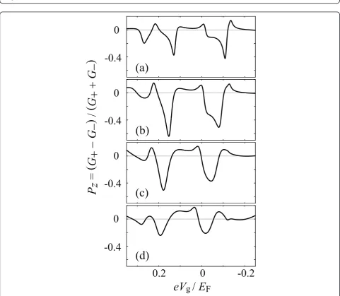
Figure 4Results of the numerical simulation for the spin-filtering device shown in Fig. 1b. The spin polarizationPzof the output current
in reservoir D1 is shown as a function of gate voltageVgon the quantum dot. The height of the tunnel barriers isUS=UD1= 0.9EF, whereas (a)
[image:5.595.57.539.316.735.2]The total conductance isGβα=Gβα+ +Gβα−, whereas the
spin polarization in thezdirection is given by
Pzβα= G βα
+ −Gβα−
Gβα+ +Gβα−
. (11)
[image:6.595.304.539.210.722.2]We focus on the transport from reservoir S to D1 and omit the superscripts (b= D1,a= S) ofGβα± and Pzba.
Figure 3 presents the conductance G± for spin sz=
±1/2 as a function of the gate voltage Vg on the QD.
We chooseUS=UD1=UD2= 0.9EFfor the tunnel
bar-riers. The conductanceG+ (solid line) and G-(broken
line) reflect the resonant tunneling through discrete energy levels formed in the QD region. Around some conductance peaks, e.g., at eVg/EF≈ 0.13 and -0.03, the
difference betweenG+ andG-is remarkably enhanced.
Thus, a large spin current is observed, which implies that two energy levels are close to each other around the Fermi level there.
The spin polarizationPzis shown in Figure 4a for the range of 0.35 >eVg/EF> -0.25. Around the conductance
peaks, a large spin polarization is observed. The effi-ciency of the spin filter becomes 37% at eVg/EF≈ 0.13
and 42% ateVg/EF≈-0.03.
Next, we examine the tuning of the spin filter by changing the tunnel coupling to lead D2. In Figure 4, we set (b)UD2/EF= 0.8, (c) 0.7, and (d) 0.6 while both
USandUD1are fixed at 0.9EF. AsUD2is decreased, the
tunnel coupling becomes stronger. First, the spin polari-zation increases with an increase in the tunnel coupling. It is as large as 63% in the case of Figure 4b. With an increase in the tunnel coupling further, the spin polari-zation decreases (Figure 4c,d).
Conclusions
We have formulated the SHE in a multi-terminal QD. The SHE is enhanced by the resonant tunneling through the QD when the level spacing is smaller than the level broadening. We have shown that the SHE is tunable by changing the tunnel coupling to the third lead. Next, the numerical simulation has been performed for a spin-filtering device using a multiterminal QD fabricated on semiconductor heterostructures. The efficiency of the spin filter can be larger than 50%.
Abbreviations
QD: quantum dot; STM: scanning tunnel microscope; SHE: spin Hall effect; SO: spin-orbit.
Acknowledgements
This work was partly supported by a Grant-in-Aid for Scientific Research from the Japan Society for the Promotion of Science, and by Global COE Program
“High-Level Global Cooperation for Leading-Edge Platform on Access Space (C12).”T. Y. is a Research Fellow of the Japan Society for the Promotion of Science.
Authors’contributions
TY participated the discussion of the analytical model and carried out the numerical calculation. ME carried out the analytical formulation of spin Hall effect. All authors conceived of the study, drafted the manuscript, read and approved the final manuscript.
Competing interests
The authors declare that they have no competing interests.
Received: 14 August 2010 Accepted: 22 June 2011 Published: 22 June 2011
References
1. ŽutićI, Fabian J, Das Sarma S:Spintronics: Fundamentals and applications.Rev Mod Phys2004,76:323.
2. Winkler R:Spin-Orbit Coupling Effects in Two-Dimensional Electron and Hole
SystemsBerlin Heidelberg: Springer; 2003.
3. Rashba EI:Properties of semiconductors with an extremum loop.1. Cyclotron and combinational resonance in a magnetic field
perpendicular to the plane of the loop.Sov Phys Solid State1960,2:1109. 4. Bychkov YuA, Rashba EI:Oscillatory effects and the magnetic
susceptibility of carriers in inversion layers.J Phys C1984,17:6039. 5. Nitta J, Akazaki T, Takayanagi H, Enoki T:Gate Control of Spin-Orbit
Interaction in an Inverted In0.53Ga0.47As/In0.52Al0.48As Heterostructure.
Phys Rev Lett1997,78:1335.
6. Grundler D:Large Rashba Splitting in InAs Quantum Wells due to Electron Wave Function Penetration into the Barrier Layers.Phys Rev Lett
2000,84:6074.
7. Sato Y, Kita T, Gozu S, Yamada S:Large spontaneous spin splitting in gate-controlled two-dimensional electron gases at normal In0.75Ga0.25As
= In0.75Al0.25As heterojunctions.J Appl Phys2001,89:8017.
8. Datta S, Das B:Electronic analog of the electro-optic modulator.Appl
Phys Lett1990,56:665.
9. Schmidt G, Ferrand D, Molenkamp LW, Filip AT, van Wees BJ:Fundamental obstacle for electrical spin injection from a ferromagnetic metal into a diffusive semiconductor.Phys Rev B2000,62:R4790.
10. Kiselev AA, Kim KW:T-shaped ballistic spin filter.Appl Phys Lett2001,
78:775.
11. Kiselev AA, Kim KW:T-shaped spin filter with a ring resonator.J Appl Phys
2003,94:4001.
12. Yamamoto M, Kramer B:A three-terminal spin filter induced by spin-orbit interaction in the presence of an antidot.J Appl Phys2008,103:123703. 13. Koga T, Nitta J, Takayanagi H, Datta S:Spin-Filter Device Based on the
Rashba Effect Using a Nonmagnetic Resonant Tunneling Diode.Phys Rev Lett2002,88:126601.
14. Eto M, Hayashi T, Kurotani Y:Spin Polarization at Semiconductor Point Contacts in Absence of Magnetic Field.J Phys Soc Jpn2005,74:1934. 15. Silvestrov PG, Mishchenko EG:Polarized electric current in semiclassical
transport with spin-orbit interaction.Phys Rev B2006,74:165301. 16. Sharma P, Brouwer PW:Mesoscopic Effects in Adiabatic Spin Pumping.
Phys Rev Lett2003,91:166801.
17. Bardarson JH, Adagideli I, Jacquod P:Mesoscopic Spin Hall Effect.Phys Rev Lett2007,98:196601.
18. Krich JJ, Halperin BI:Spin-polarized current generation from quantum dots without magnetic fields.Phys Rev B2008,78:035338.
19. Krich JJ:Fluctuations of spin transport through chaotic quantum dots with spin-orbit coupling.Phys Rev B2009,80:245313.
20. Murakami S, Nagaosa N, Zhang S-C:Dissipationless Quantum Spin Current at Room Temperature.Science2003,301:1348.
21. Sinova J, Culcer D, Niu Q, Sinitsyn NA, Jungwirth T, MacDonald AH:
Universal Intrinsic Spin Hall Effect.Phys Rev Lett2004,92:126603. 22. Wunderlich J, Kaestner B, Sinova J, Jungwirth T:Experimental Observation
of the Spin-Hall Effect in a Two-Dimensional Spin-Orbit Coupled Semiconductor System.Phys Rev Lett2005,94:047204.
23. Dyakonov MI, Perel VI:Current-induced spin orientation of electrons in semiconductors.Phys Lett1971,35A:459.
24. Engel HA, Halperin BI, Rashba EI:Theory of Spin Hall Conductivity in n-Doped GaAs.Phys Rev Lett2005,95:166605.
26. Eto M, Yokoyama T:Enhanced Spin Hall Effect in Semiconductor Heterostructures with Artificial Potential.J Phys Soc Jpn2009,78:073710. 27. Yokoyama T, Eto M:Enhanced spin Hall effect by tuning antidot
potential: Proposal for a spin filter.Phys Rev B2009,80:125311. 28. Yokoyama T, Eto M:Spin filter due to spin Hall effect with axially
asymmetric potential.Physica E2010,42:956.
29. Igarashi Y, Jung M, Yamamoto M, Oiwa A, Machida T, Hirakawa K, Tarucha S:Spin-half Kondo effect in a single self-assembled InAs quantum dot with and without an applied magnetic field.Phys Rev B
2007,76:081303(R).
30. Fasth C, Fuhrer A, Samuelson L, Golovach VN, Loss D:Direct Measurement of the Spin-Orbit Interaction in a Two-Electron InAs Nanowire Quantum
Dot.Phys Rev Lett2007,98:266801(R).
31. Vachon M, Raymond S, Babinski A, Lapointe J, Wasilewski Z, Potemski M:
Energy shell structure of a single InAs/GaAs quantum dot with a spin-orbit interaction.Phys Rev B2009,79:165427.
32. Pfund A, Shorubalko I, Ensslin K, Leturcq R:Dynamics of coupled spins in quantum dots with strong spin-orbit interaction.Phys Rev B2009,
79:121306(R).
33. Takahashi S, Igarashi Y, Deacon RS, Oiwa A, Shibata K, Hirakawa K, Tarucha S:Quantitative evaluation of spin-orbit interaction in InAs quantum dots.J Phys Conf Ser2009,150:022084.
34. Takahashi S, Deacon RS, Yoshida K, Oiwa A, Shibata K, Hirakawa K, Tokura Y, Tarucha S:Large Anisotropy of the Spin-Orbit Interaction in a Single InAs Self-Assembled Quantum Dot.Phys Rev Lett2010,104:246801.
35. Datta S:Electronic Transport in Mesoscopic SystemsCambridge: Cambridge University Press; 1995.
36. Meir Y, Wingreen NS:Landauer formula for the current through an interacting electron region.Phys Rev Lett1992,68:2512.
37. Eto M, Yokoyama T:Quantum Dot Spin Filter in Resonant Tunneling and Kondo Regimes.J Phys Soc Jpn2010,79:123711.
38. Ando T:Quantum point contacts in magnetic fields.Phys Rev B1991,
44:8017.
39. Yamamoto M, Ohtsuki T, Kramer B:Spin polarization in a T-shaped conductor induced by strong Rashba spin-orbit coupling.Phys Rev B
2005,72:115321.
doi:10.1186/1556-276X-6-436
Cite this article as:Yokoyama and Eto:Efficient spin filter using multi-terminal quantum dot with spin-orbit interaction.Nanoscale Research Letters20116:436.
Submit your manuscript to a
journal and benefi t from:
7 Convenient online submission
7 Rigorous peer review
7 Immediate publication on acceptance
7 Open access: articles freely available online
7 High visibility within the fi eld
7 Retaining the copyright to your article