PAPER • OPEN ACCESS
A Study of 4-level DC-DC Boost Inverter with
Passive Component Reduction Consideration
To cite this article: A. N. Kasiran et al 2018 J. Phys.: Conf. Ser. 995 012062
View the article online for updates and enhancements.
Related content
Chaos minimization in DC-DC boost converter using circuit parameter optimization
N Sudhakar, Rajasekar Natarajan, Kumar Gourav et al.
-Chaos control in solar fed DC-DC boost converter by optimal parameters using nelder-mead algorithm powered enhanced BFOA
N Sudhakar, N Rajasekar, Saya Akhil et al.
-A new active power filter topology based on a chopper circuit
Xiao-Ling Guo, Jian Cheng, Bo Zhang et al.
A Study of 4-level DC-DC Boost Inverter with Passive
Component Reduction Consideration
A. N. Kasiran
1, A. Ponniran
1, M. A. Harimon
1, H. H. Hamzah
1 1Faculty of Electrical and Electronic Engineering, Universiti Tun Hussein Onn Malaysia, 86400, Parit Raja, Johor, Malaysia.Abstract.This study is to analyze design principles of boost inductor and capacitor used in the 4-level DC-DC boost converter to realize size reduction of passive component referring to their attributes. The important feature of this circuit is that most of the boost-up energy is transferred from the capacitor-clamped to the output side which the small inductance can be used at the input side. The inductance of the boost inductor is designed by referring the inductor current ripple. On the other hand, the capacitance of the capacitor-clamped is designed by considering voltage stress on semiconductor devices and also the used switching frequency. Besides that, according to the design specifications, the required inductance in 4-level DC-DC boost converter is decreased compared to a conventional conventional DC-DC boost converter. Meanwhile, voltage stress on semiconductor device is depending on the maximum voltage ripple of the capacitor-clamped. A 50 W 4-level DC-DC boost converter prototype has been constructed. The results show that the inductor current ripple was 1.15 A when the inductors, 1 mH and 0.11 mH were used in the conventional and 4-level DC-DC boost converters, respectively. Thus, based on the experimental results, it shows that the reduction of passive components by referring to their attributes in 4-level DC-DC boost converter is achieved. Moreover, the decreasing of voltage stress on the semiconductor devices is an advantage for the selection of low ON-resistance of the devices which will contribute to the reduction of the semiconductor conduction loss. The integration result of boost converter and H-bridge inverter is also shown.
1. Introduction
2
design principle of passive components which is inductors and capacitors in multilevel DC-DC boost converters. Conventional conventional and 4-level DC-DC boost converters are considered for a boost inverter system in this study. The principles of conventional and 4-level boost DC-DC converters are defined. Then, the design of inductor and capacitor are discussed for both converters. The simulation and experimental results of the conventional and 4-level DC-DC converters are analyzed and discussed for the design parameters confirmation.
2. 4-level DC-DC Boost Inverter System
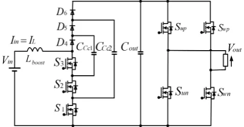
[image:3.595.171.410.308.432.2]In the boost inverter system of this study, 4-level DC-DC boost converter is integrated with H-bridge inverter circuits as shown in Figure 1. The renewable energy source is considered constant where an open loop system is considered. The main interest of this study is 4-level DC-DC boost converter which it has similar characteristics with conventional conventional DC-DC boost converter. Even though, 4-level DC-DC boost inverter is known as a double stage system, the advantage of the multilevel structure topology is able to overcome the bulky problem of passive components.
Figure 1.4-level DC-DC boost inverter system.
3. Principle of 4-level DC-DC Boost Converter
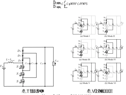
Basically, 4-level DC-DC boost converter consists of one boost inductorL, two capacitor-clampedCC, one output capacitorCoutand six semiconductor devices, as shown in Figure 2(a). The output voltage Vout is expressed by (1), meanwhile the boost ratio is expressed by (2). Thus the duty ratio D is controlled in order to varies the output voltageVout.
in out V
V (1)
D
1 1
(2)
Figure 2 (b) shows the operation modes of the 4-level DC-DC boost converter. Basically the 4-level DC-DC boost converter has six operation modes. In this study the boost ratiois equal to 2 (Dequal to 0.5) is considered.
4. Components Design Consideration
4.1. Inductor design principle
L L
L T
L V I
(3)
whereVLis the inductor voltage andTLis the charging time of the inductor.
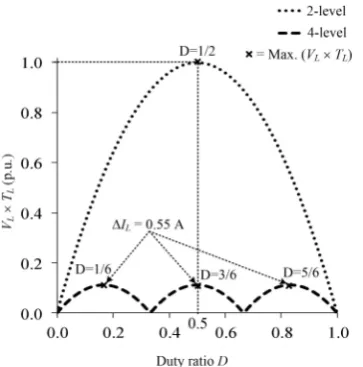
Besides, in order to achieve maximum inductor current ripple∆IL, the maximum product ofVL andTLmust be achieved. Figure 3 shows the relationship between the product (VLandTL) against the duty ratio D for conventional and 4-level DC-DC boost converters. The maximum inductor current ripple is achieved at D equal to 1/2 (VL TL is maximum). However, in the 4-level DC-DC boost converter it has three maximum current ripple when the duty ratios are 1/6, 3/6 and 5/6. Due to the lower value of maximum points of VL TL, the inductance is reduced in 4-level DC-DC boost converter. Thus, the boost inductor in the conventional and 4-level boost converters are expressed as follows respectively,
) 2 (
2 2 2 1
level L out level V T I L
(4)
) 4 (
4 6 6 1
level L out level V T I L
(5)
If the inductance of the conventional DC-DC boost converter and in the 4-level DC-DC boost converter is compared with the same specifications, the ratio of between 4-level and conventional DC-DC boost converters ia expressed in (5). The 4-level DC-DC-DC-DC boost converter required only 11.11% of the inductance.
% 11 . 11 1111 . 0 9 1 2
4
level level L
L (6)
[image:4.595.78.511.410.736.2](a) Main circuit (b) Operation mode
4
Figure 3. Relationship between VL × TL (p.u.) and D in the conventional and 4-level DC-DC boost converters.
4.2. Design of Capacitor-clamped principle
The voltage stress on switching devices can estimated by referring to the capacitor-clamped CC voltage. Switching frequency must be considered as well in estimating the capacitance. Basically, the voltage across capacitor-clamped are expressed follow,
out level Cc V V 3 1 ) 4 (
1 (7)
out level Cc V V 3 2 ) 4 (
2 (8)
The minimum capacitances CCc1 and CCc2 in the 4-level DC-DC boost converter are expressed as follow,
c level out
in sw inlevel
Cc V P DV V f
C 2 6 3 max ) 4 ( 1 ) 4 (
1
(9)
c level out
in sw inlevel
Cc V V V f
D P C 4 6 3 max ) 4 ( 2 ) 4 (
2
(10)
The maximum voltage stress on semiconductor device in 4-level DC-DC boost converter is expressed as follows, sw level Cc in in out level
sw V C f
D P V V min ) 4 ( 1 max 4
( 31 21
(11)
5. Results and analysis
Table 1.Specifications in the simulation and experiment for conventional and 4-level DC-DC boost converter.
Specifications Value
Output power,P 50 W
Inductor current,Iin 1.06 A
Input voltage,Vin 50 V
Output voltage,Vout 100 V
Switching frequency,fsw 22 kHz
Duty ratio,D 0.5
Boost inductance,LB 1 mH
Capacitor-clamped,CCc 470 µF
Output capacitor,Cout 470 µF
MOSFET IRF840N
Diode BYT79
5.1. Inductor current ripple, ∆IL
The inductor current ripple is observed by using the same boost inductance (L = 1 mH) for both converters. The inductor current ripple is designed at 127.42 mA for 4-level DC-DC boost converter meanwhile 1.15 A for the conventional boost converter. The simulation result shows a good agreement between design and simulation results as shown in Figure 4. It strengthened by the experimental result where the current ripple is approximately same with the simulation and design current ripple shown in Figure 5.
Figures 4 and 5 show the simulation and experimental results. Both results show a good agreement. The current ripple is approximately 127-128 mA (D = 0.5) from the simulation and experimental results in the 4-level DC-DC converter. Meanwhile, Figure 4(b) shows the current ripple is approximately 1.14-1.15 A from the simulation and experimental results in the conventional DC-DC converter. Thus the inductor current ripple is reduced in the 4-level DC-DC converter.
[image:6.595.102.469.475.646.2](a) 4-level DC-DC boost converter. (b) conventional DC-DC boost converter.
6
[image:7.595.85.488.108.267.2](a) 4-level DC-DC boost converter (b) conventional DC-DC boost converter
Figure 5. Experimental results of the capacitor output voltage, capacitor-clamped voltage, input voltage and inductor current ripple (Cout= 470 µF,CCc=470 µF,L =1 mH).
5.2. Inductor voltage, VL
In the conventional DC-DC converter, when D is 0.5, charging time of the inductor is half of switching period. This also occurred at the inductor voltage VL where the value becomes half of the output voltageVout. However, in the 4-level DC-DC boost converter, the inductor voltage becomes 1/6 of the output voltage and similar for the charging times of the inductor. Figure 6 shows the inductor voltage for 4-level DC-DC boost converter and conventional DC-DC boost converter and the results were confirmed with the designed values. The inductor voltage in the 4-level DC-DC boost converter needs only 33.3% of the conventional boost converter. Thus, the results of simulation and experimental show a good agreement.
(a) 4-level DC-DC boost converter (b) Conventional DC-DC boost converter
Figure 6.Experimental waveforms of inductor voltage and inductor current.
5.3. Relationship between capacitance of the capacitor-clamped and output voltage ripple
[image:7.595.98.483.419.559.2](a)CC1= CC2=200 µF (b)CC1= CC2=50 µF (c)CC1= CC2=10 µF Figure 7.Simulation waveforms of capacitor output voltage, capacitor-clamped voltage and
inductor current with variation of the capacitances of the capacitor-clamped.
5.4. Voltage stress on semiconductor device
In 4-level DC-DC boost converter, the voltage rating of the semiconductor device must greater than the maximum voltage of capacitor-clamped during operation. This is due to the charging condition of the capacitor-clamped where it reached the maximum value in certain mode operation. Thus, the voltage across on the semiconductor device can be based on the parallel connection with the capacitor-clamped. The switching frequency used is also influenced the design of the capacitor. When a high switching frequency is used, it will cause the time period become smaller, thus the time of charging and discharging of capacitor-clamped is reduced as well. It confirmed in the simulation results, when high switching frequency is used, the capacitor voltage ripple reduces and smaller capacitance can be used.
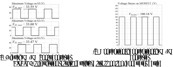
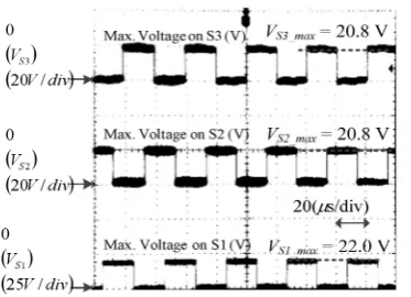
The conventional conventional DC-DC boost converter is suffered from high voltage stress on semiconductor devices due to parallel connection to output side. From the simulation result, it shows in Figure b(b), the MOSFET voltage is approximately same as the output voltage. Thus, the voltage rating of the semiconductor device use must be higher in order to withstand high voltage stress. However, the voltage stress on semiconductor device in 4-level DC-DC boost converter was greatly reduced. This is due to additional of semiconductor devices are used in 4-level DC-DC boost converter circuit. Figure 8(a) shows the voltage stress on the semiconductor devices is approximately same of the capacitor-clamped voltage, 33 V. The voltage stress on a semiconductor device in 4-level DC-DC boost converter is divided by three of the output voltage. In the experimental results, the input voltage is reduced by half due to the safety purposes. The output voltage was approximately 55 V. Figure 9 shows it is confirmed that the voltage stress on semiconductor devices are reduced greatly in 4-level DC-DC boost converter. The problems of improper charging and discharging of capacitor-clamped is reduced by considering a natural balancing circuit.
(a) 4-level DC-DC boost converter (b) Conventional conventional DC-DC boostconverter
[image:8.595.115.478.621.763.2]8
(Vin=50 V, LB= 1 mH, D= 0.5).
[image:9.595.79.266.190.325.2]6. Integration
Figure 10 shows the results of the boost inverter system which the output of the boost inverter system is boosted in sinusoidal waveform as expected.
Figure 9.Experimental results of voltage stress on semiconductor device (MOSFET) in 4-level DC-DC boost converter circuit,Vout=
[image:9.595.322.459.192.326.2]55 V.
Figure 10.Simulation result of 4-level DC-DC boost inverter system after integration.
Acknowledgment
The authors would like to express their deepest appreciation to the Ministry of Higher Education and Universiti Tun Hussein Onn Malaysia for supporting this research under Research and Innovation Fund. Many thank are due to all research members for their tremendous work and cooperation.
7. Conclusion
In this paper, the authors have discussed the design of passive components referring to their attributes in the 4-level DC-DC boost converter in order to solve the bulky problem of passive components which is suffered in conventional DC-DC boost converter. It confirmed that the inductance of the boost inductor can be reduced greatly in 4-level DC-DC boost converter. Besdes, the simulation and experimental results show that the voltage stress on semiconductor devices in 4-level DC-DC boost converter circuit is reduced due to additional semiconductor devices and passive components. For the future works, closed loop control strategies may have applied to control power pulsation problem and unbalanced of the capacitor-clamped voltages.
Reference
[1] H. Watanabe, K. Kusaka, K. Furukawa, K. Orikawa, and J. I. Itoh, “DC to single-phase AC Voltage Source Inverter with power decoupling circuit based on flying capacitor topology for PV system,” Conf. Proc. - IEEE Appl. Power Electron. Conf. Expo. - APEC, vol. 2016– May, pp. 1336–1343, 2016.
[2] R. O. Cáceres and I. Barbi, “A boost DC-AC converter: Analysis, design, and experimentation,” IEEE Trans. Power Electron., vol. 14, no. 1, pp. 134–141, 1999.
[3] J. Kan, S. Xie, and Y. Wu, “Single-Stage and Boost-Voltage Grid-Connected Inverter for Fuel-Cell Generation System,” vol. 62, no. 9, pp. 5480–5490, 2015.
[4] A. B. Ponniran, K. Matsuura, K. Orikawa, and J.-i. Itoh, "Size Reduction of DC-DC Converter using Flying Capacitor Topology with Small Capacitance," IEEJ Journal of Industry Applications, vol. 3, pp. 446-454, 2014.
2011, pp.1315–1322, 2011.
[6] Y. Jang and M. M. Jovanović, “Interleaved boost converter with intrinsic voltage-doubler characteristic for universal-line PFC front end,” IEEE Trans. Power Electron., vol. 22, no. 4, pp. 1394–1401, 2007.
[7] S. Y. Tseng, J. Z. Shiang, H. H. Chang, W. S. Jwo, and C. T. Hsieh, “A novel turn-on/off snubber for interleaved boost converters,” PESC Rec. - IEEE Annu. Power Electron. Spec. Conf., pp. 2341–2347, 2007.
[8] H. Keyhani and H. A. Toliyat, “Flying-capacitor boost converter,” Conf. Proc. - IEEE Appl. Power Electron. Conf. Expo. - APEC, pp. 2311–2318, 2012.
[9] F. Zhang, F. Z. Peng, and Z. Qian, “Study of the multilevel converters in DC-DC applications,” Power Electron. Spec. Conf. 2004. PESC 04. 2004 IEEE 35th Annu., vol. 2, p. 1702–1706 Vol.2, 2004.
[10] A. B. Ponniran, K. Orikawa and J. Itoh, "Minimum Flying Capacitor for N-Level Capacitor DC/DC Boost Converter," in IEEE Transactions on Industry Applications, vol. 52, no. 4, pp. 3255-3266, July-Aug. 2016.
[11] A. B. Ponniran, K. Orikawa, and J.-i. Itoh, "Minimization of Passive Components in Multi-level Flying Capacitor DC-DC Converter," IEEJ Journal of Industry Applications, vol. 5, pp. 10-11, 2016.
[12] R. Das, “PI Controlled Bi-Directional DC-DC Converter ( BDDDC ) and Highly Efficient Boost Converter for Electric Vehicles,” 2016.
[13] K. F. Krommydas and A. T. Alexandridis, “A New Design Approach of Stable Nonlinear PI Controllers for Stand-Alone Photovoltaic Systems,” pp. 1458–1463, 2013.