ISSN: 2278 – 7798 All Rights Reserved © 2014 IJSETR 2687
DESIGN OF TEST PATTERN OF
MULTIPLE SIC VECTORS FROM LOW
POWER LFSR THEORY AND
APPLICATIONS IN BIST SCHEMES
P. SANTHAMMA ,
T.S. GHOUSE BASHA , B.DEEPASREEABSTRACT--- BUILT-IN SELF-TEST (BIST) techniques can effectively reduce the complexity of VLSI testing, by introducing on-chip test hardware into the circuit-under-test (CUT). In BIST architectures, the linear feedback shift register (LFSR) is commonly used in the test pattern generators (TPGs) and output response analyzers. A major drawback of these architectures is that the pseudorandom patterns generated by the LFSR lead to significantly high switching activities in the CUT, which can cause excessive power dissipation. This drawback can be reduced by using Low Power LFSR. In this paper the Low Power LFSR generates the Test Pattern for BIST by using the MSIC vectors. This will improve the Performance of BIST rather than the previous techniques of using LFSR and Twisted ring Counters. The test time and data volume required for test pattern generation is also reduced in this technique. It is flexible to both Test per Scan and Test per Clock techniques. INDEX TERMS- BIST,CUT,LFSR,LOWPOWER LFSR,TPG.
Manuscript received October, 2014:
P.Santhamma, Assistant professorDepartment of ECE,K.O.R.M.C.E,JNTUA Kadapa,India.
T.S.Ghouse Basha,Assosiate professor Department of ECE,K.O.R.M.C.E,JNTUA Kadapa, India. B. Deepasree Mtech student,Department of ECE,K.O.R.M.C.E,JNTUA Kadapa, India.
I. INTRODUCTION
BIST technology that embeds some specific test structure into a circuit-under-test (CUT) has been proposed to reduce the total test cost .Previous BIST methods can generally be classified into test per-scan and test-per-clock ones according to their test application schemes. The test-per-scan method serially loads one test pattern into scan chains bit-by-bit. Therefore large test application time on pattern loading is required, especially when the scan chain length is long. The test-per-clock method applies one test pattern for each test cycle and all output responses corresponding to one test pattern are captured and loaded to a parallel response monitor simultaneously. Though the area overhead required for the response monitor may be large, the test-per-clock schemes do have the advantage of much shorter test time since one test pattern can be applied for each clock cycle. Therefore in the applications where the area overhead is not the main concern while test time is, test-per-clock can become a good choice for testing. In this paper, we focus on the test-per-clock BIST Method
ISSN: 2278 – 7798 All Rights Reserved © 2014 IJSETR 2688
Figure 1. (a) Test per Clock (b) Test per Scan
II.TRC BASED TEST GENERATION SCHEME
As Figs. 2(a) and (b) show, an m-bit ring counter (RC)consists of an m-bit shift register and a feedback path from the output of the last flip-flop to the input of the first flip flop, and an m-bit TRC is similar to an
m-bit ring counter except that an inverter is inserted
on the feedback path. With an initial state, maximally
m and 2m different test patterns can be generated by
using an m-bit RC and a TRC, respectively. Fig. 2(c) shows a combination of an RC and a TRC. By setting the control signal ctrl, one can switch between the RC and the TRC modes. The PTRC design proposed in this paper is based on the design shown in Fig. 2(c), which can generate the maximum number of different test patterns, i.e., maximally 3m patterns can be generated by an m-bit PTRC. In addition, the PTRC can also be programmed to perform different orders of operations such that more pattern generation flexibility can be achieved. With this scheme, both the storage data volume and test application time can be significantly reduced. Furthermore, we shall divide a long shift register into multiple segments a convert each segment into a
PTRC. By concurrently generating test patterns for all segments with different control signals we show that the test application time can be further and greatly reduced. Fig 3 shows the proposed programmable multiple TRC scheme which consists of a centralized mode switching logic unit and a set of PTRC logic units with a reversion logic unit associated with each PTRC unit. In this scheme, all primary inputs and internal storage elements in the CUT are combined together and partitioned into n equal-length scan segments, where n is a user-defined parameter. For example, the PTRC scheme shown in Fig. 2 contains two scan segments. PTRC logic unit contains a 2-to-multiplexer and a3-input XOR gate in front of the scan input of each m-bit scan segment, where m is the number of scan cells in a scan segment. One reversion logic unit with a one-bit control pin is employed for each PTRC unit. Since these hardware units are quite simple, the area overhead is small. Also since these units are not on the critical paths of the CUT, almost no performance degradation is induced. The whole test generation process of the proposed scheme is managed by the logic units. Under the concurrent control of these units, all PTRC designs can jointly generate the required test patter at the same time so as to reduce test application time. On the other hand, by appropriately adjusting the control signal for each individual reversion logic unit, different TRCs can be separately programmed to perform different orders of test generation modes and thus more effective patterns can be generated, which leads to significant reduction of the total storage data volume, mode switching logic unit and the reversion
ISSN: 2278 – 7798 All Rights Reserved © 2014 IJSETR 2689
III.LINEAR FEED BACK SHIFT REGISTER Linear feedback shift register is a circuit used here to generate test pattern for Bist.These patterns are used to determine the circuit is faulty circuit or not.
Fig. 2. (a) m-bit ring counter, (b) m-bit twisted ring counter, and
(c) Combination of (a) and (b).
Figure 3. Example of the programmable and multiple twisted-ring counters based test architecture (two
scan segments, n = 2)
Test Pattern of LFSR for BIST:
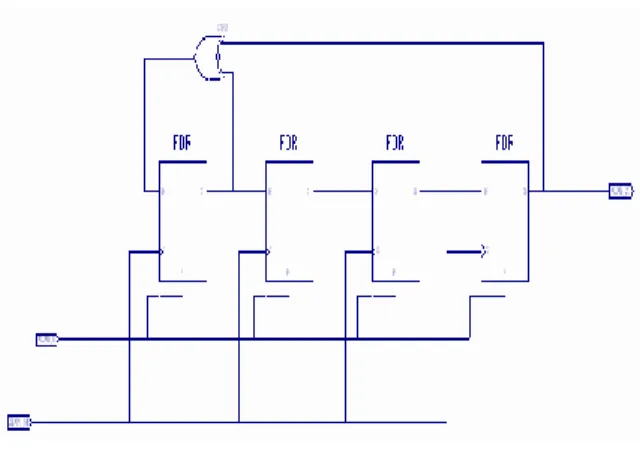
Linear Feedback Shift Register is a circuit having of flip-flops that are connected in series with each other is shown in fig 4. The output of first flip-flop is connected to the input of the second flip flop and connection is going upto the last flip flop. The Characteristic polynomial can be obtained from the feedback polynomial. This feedback polynomial is used to determine the length of Test patterns. In this LFSR the switching activity increases which may cause excessive power usage. This can be reduced by using low power.
Figure 4. LFSR
Test Pattern Generation of Low power LFSR The idea behind low power test pattern generation is to improve the correlation between the bits of successive vectors is to reduce the switching activities of logic levels.
The new approach entails inserting 3 intermediate vectors between every two successive vectors. The total number of signal transitions between these 5 vectors is equal to the total number of signal transitions between the 2 successive vectors generated using the conventional approach. This reduction of signal transition activity in the primary inputs reduces the switching activity inside the design under test and therefore results in reduced power Consumption by the device under test.
ISSN: 2278 – 7798 All Rights Reserved © 2014 IJSETR 2690 Procedure for the technique to produce low power
pattern for BIST:
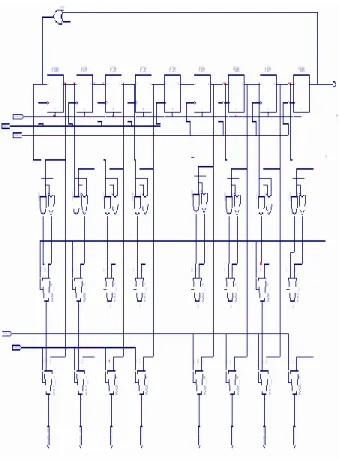
Fig: 5.Low power LFSR circuit
The procedure for generating the low power lfsr Test pattern is described as fallows.
The description consists of generating of test pattern vectors T1,T2…etc. Each vector consists of three intermediate vectorsTa,Tb,Tc that have to generate after generating the first vector.
Here the pattern generation is a 9-bit lfsr pattern generation.To generate the first vector T1,the clock is enabled for first four bits of Lfsr and not clocking for last four bits of Lfsr outputs. And we have to assume intial output states(for ex:01001011). It first shifts the first four bits to the right by one bit.The feedback bits of Lfsr are the outputs of eighth and first flipflop.By taking the exclusive-or of the values
of outputs of eighth and first flipflop ,the result is giving as ainput of the first flipflop.The shaded register is the fifth flipflop register and it is clocked along with the first four bits of Lfsr.Input of the Shaded register is the output of the fourth flipflop. The intermediate vectors of Ta,Tb,Tc are generated next from T1.
Ta is generated by disabling the clock to the first four bits of Lfsr outputs and not clocking to the last four bits.and last four are ouputs of the injector circuit.The injectot circuit is to compare the next value with current value.
Tb is genearated by shifting the last four bits to the right one bit by clock enabling,but do not shifting the first four bits by disabling the clock.
Tc is generated by disabling the complete LFSR.First four bits outputs are propagate from the injection circuit,last four bits are same as Tb.
Generating T2 is quite same as T1.As in Tc from T1 and taking outputs of first four flipflops are the current values ,the seed vector for T2 is generated.Then by clocking the first four bits,it shifts first four bits and shaded flipflop bit and disabling the last four flipflop.
The concept of Low power pattern generation can be extended to 36 bits required for the design circuit.
ISSN: 2278 – 7798 All Rights Reserved © 2014 IJSETR 2691
Fig: 6..BIST Architecture using LFSR Here the LFSR is used as the Low power LFSR to generate test pattern.
IV.SIMULATION RESULT
Fig: 7.Simulation output of BIST using low power LFSR
The simulation gives the test pattern of Low power LFSRs in BIST,these are used to test circuit on Chip in vlsi designs
Design summary:
Sythesis Report:
V.CONCLUSION
The Low power Linear feedback shift register generates test patterns are easy in obtaining and this is effectively increase the performance of on chip testing. As these patterns obtaining is simple, the data volume required for storing the test patterns can be reduced. This technique can be enhanced with complete fault coverage measurement and reducing test cycle.
ISSN: 2278 – 7798 All Rights Reserved © 2014 IJSETR 2692 Acknowledgements
B.Deepasree would like to thank Mr.T.S. Ghouse Basha,Head of department and Mrs. P.Shantamma, assistant professor in ece dept,who had been guiding through out the project and supporting me in giving technical ideas about paper and motivating me to complete then work efficiently and successfully REFERENCES
[1] Patrick Girard, “Survey of Low-Power
Testing of VLSI Circuits, IEEE Design and Test of Computers, May-June 2002, Volume: 19 , Issue: 3, page(s): 80 – 90, ISSN: 0740-7475
[2] S. Zhang, et. al, “Cost driven optimization of fault coverage in combined built-In-Self-Test/Automated Test Equipment Testing”, IEEE Instrumentation and Measurement Technology Conference, May 18-20, 2004 [3] L. Ungar and T. Ambler, “Economics of
Built-In-Self-Test”, IEEE Design and Test of Computers, Sept.-Oct. 2001, Volume: 18 , Issue: 5, page(s): 70 – 79, ISSN: 0740-7475
[4] Benoit Nadeau-Dostie, “Design for
AT-SPEED TEST, DIAGNOSIS and
MESUREMENT, ISBN 0-7923-8669-8
B.DEEPASREE is presently pursing M Tech in VLSI in K.O.R.M. College, kadapa. She has completed Bachelor of Technology in Electronics and Communication Engineering from K.O.R.M Engineering College of JNTU University in 2011.She worked as Assistant Professor in RVPW Engineering College Kadapa. Her areas of interest include VLSI Testing, IC Designs
P.SANTHAMMA is presently working as Assistant professor in the department of Electronics and Communication Engineering in KORM College of Engineering, Kadapa. She working in teaching field since 7 years.She received her B.tech and M.tech degree from the department of ECE from JNTU and JNTU Kakinada.Her areas of
interest include signal processing and
communications.
T.S.GHOUSE BASHA is
presently working as an Associate Professor and HOD in the Department of Electronics and Communication Engineering in KORM College of Engineering, Kadapa. He carried out his MTech project work in Defence Research and Development Laboratory, Hyderabad and working in teaching field since eleven years in different cadres. He received his BTech and MTech from the Department of Electronics and Communication Engineering from JNTU University and Nagarjuna University respectively.He has submitted his Ph D thesis in microwave antennas to JNTUA. His areas of interest include microwave antennas, digital signal processing and mobile communications