Analysis and Design Aspects of a Series Power
Semiconductor Array with Digital Waveform
Control Capability for Single Phase AC Voltage
Regulators and Other Applications
Nihal Kularatna, Chandani Jindasa The University of Waikato, Hamilton, New Zealand
E-mail: [email protected]
Received May 17,2011; revised June 15, 2011; accepted June 22, 2011
Abstract
A series connected power semiconductor array, with digital control capability could be used for developing single phase AC regulators or other applications such as AC electronic loads. This technique together with an ordinary gapless transformer could be used to develop a low cost AC voltage regulator (AVR) to provide better or comparable specifications with bulky ferro-resonant AVR types. One primary advantage of the technique is that digital control can be used to minimize harmonics. Commencing with a review of AC volt-age regulator techniques for single phase power conditioning systems, an analysis and design aspects of this technique is presented with experimental results for AVRs. Guidelines on how to utilize the technique in a generalized basis is also summarized together with a summary of a technique for achieving harmonic con-trol.
Keywords:Power Conditioners, AC Voltage Regulators (AVR), Power Semiconductors, Digital Control, Electronic AC Loads
1. Introduction
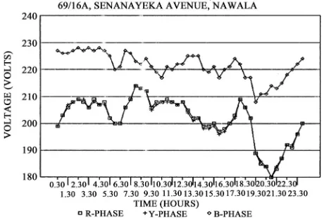
With the proliferation of electronic systems based on submicron feature transistors, power quality (PQ) has become a major concern for end users as well as distri-bution authorities around the world [1-6]. Voltage sags and surges are a very common phenomenon in many distribution circuits, and it is particularly so in over-loaded distribution systems. Voltage sags and surges seem to be distributed and tend to follow the daily load-ing patterns of the utility [2]. Extreme voltage fluctua-tions in many developing countries [7] and the need for lower cost products with easy manufacturability moti-vated the preliminary R & D work related to this spe-cific technique. Figure 1 indicates a typical pattern of voltage fluctuations in an urban location sub-circuit in Sri Lanka [7].
To improve the quality of power at the end user prem-ises, three major considerations are voltage sags and surges, transient surges such as lightning or inductive energy dumps, and harmonics and flicker etc. An AC
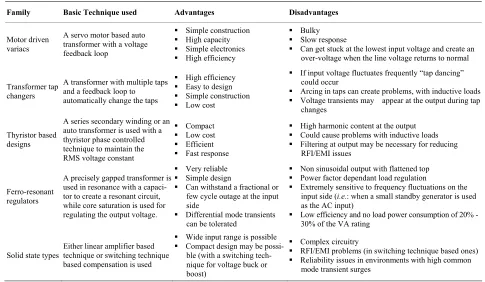
[image:1.595.309.539.530.686.2]Voltage Regulator (AVR) is a particularly useful power conditioning equipment. The common AVR techniques used are: 1) motor driven variacs; 2) transformer tap changers; 3) ferro resonant regulators; 4) thyristor based
systems (v) solid state AC regulators. Table 1 summa-rizes the performance of these commercial families in a practical stand point in order to compare with the new technique we introduce in the paper. The information is particularly applicable to the single phase systems used by the end users and with output ratings from few 100Watts to few kilowatts. Magnetic amplifier tech-niques [8] usable in large capacity single or 3 phase sys-tems etc are not discussed here.
Given the above variety of techniques used in com-mercial circumstances [9], a consistently popular tech-nique has been the ferro-resonant type. Invented by Jo-seph Sola in the 1930s, this technique is popular due to its operational reliability, simple construction, and the ability to ride through a couple of AC cycles. However, this line frequency tuned LC resonant circuit based technique has the following disadvantages: 1) dissipates approximately 150 - 250 watts per each KVA of its output, due to the gapped transformer operating near saturation; 2) output regulation is dependant on the power factor of the con-nected load [10]; 3) various malfunctions when powered by a standby generator where the output frequency fluc-tuates with the load (due to LC circuit operating beyond resonance). Item 3) was a common occurrence in Sri Lanka during the drought periods with long power out-ages, where the first part of the work presented in the paper was carried out. In these cases frequent malfunc-tions of some commercial line interactive type UPS
sys-tems with ferro based AVRs were a common occurrence. Apart from the above approaches used in commercial AVR techniques, there are few other published ap-proaches to achieve AC voltage regulation in single phase power conditioners. Many of these are based on a series AC voltage component generated by a switching PWM scheme [11,12], or electronic transformers, which are also based on a PWM switching technique [13,14]. Another variation of a PWM based series connected AC regulator technique is described in [15,16]. The common problem in these are RFI/EMI due to PWM switching schemes, and the complex cost and manufacturing issues of adapting them to output power levels from few 100W to few kilowatts in single phase environments.
Given the above summary, key requirements in de-veloping AVR techniques suitable for modern power conditioning requirements could be summarized as:
a) Reliability of operation in surge-prone PQ envi-ronments;
b) Efficiency under all load levels and load power factor situations;
c) RFI/EMI minimization; d) Output harmonic minimization;
e) Speed of the control loops within the regulator; f) Operability within the extremes of input line voltage limits;
[image:2.595.54.539.441.723.2]g) Energy storage for short duration ride through re-quirements.
Table 1. Comparison of AC voltage regulators.
Family Basic Technique used Advantages Disadvantages
Motor driven variacs
A servo motor based auto transformer with a voltage feedback loop
Simple construction
High capacity
Simple electronics
High efficiency
Bulky
Slow response
Can get stuck at the lowest input voltage and create an over-voltage when the line voltage returns to normal
Transformer tap changers
A transformer with multiple taps and a feedback loop to automatically change the taps
High efficiency
Easy to design
Simple construction
Low cost
If input voltage fluctuates frequently “tap dancing” could occur
Arcing in taps can create problems, with inductive loads
Voltage transients may appear at the output during tap changes
Thyristor based designs
A series secondary winding or an auto transformer is used with a thyristor phase controlled technique to maintain the RMS voltage constant
Compact
Low cost
Efficient
Fast response
High harmonic content at the output
Could cause problems with inductive loads
Filtering at output may be necessary for reducing RFI/EMI issues
Ferro-resonant regulators
A precisely gapped transformer is used in resonance with a capaci-tor to create a resonant circuit, while core saturation is used for regulating the output voltage.
Very reliable
Simple design
Can withstand a fractional or few cycle outage at the input side
Differential mode transients can be tolerated
Non sinusoidal output with flattened top
Power factor dependant load regulation
Extremely sensitive to frequency fluctuations on the input side (i.e.: when a small standby generator is used as the AC input)
Low efficiency and no load power consumption of 20% - 30% of the VA rating
Solid state types
Either linear amplifier based technique or switching technique based compensation is used
Wide input range is possible
Compact design may be possi-ble (with a switching tech-nique for voltage buck or boost)
Complex circuitry
RFI/EMI problems (in switching technique based ones)
2. AC Power Control Technique Based on a
Series Power Semiconductor Array
Given the above introduction to the commercial design approaches with key design requirements in AVRs, fol-lowing section introduces the primary design concepts used in this technique. The technique discussed in this paper was developed for single phase end user equip-ment where the line voltage could fluctuate widely and to achieve a design without any ferro-resonant transformers for easy manufacturability.
This technique based on a series connected power semiconductor array [17-20] is suitable for situations where 230V AC rms voltage fluctuates widely between 160 V to 260 V. The technique has the following advan-tages and useful features:
1) Fast response and high efficiency at worst case sags 2) Gapless 50/60 Hz transformer;
3) True RMS output control;
4) Electrical isolation between low voltage control circuits and the power stage;
5) Minimum RFI/EMI issues;
6) Lower harmonic distortion at output and less de-pendence on the load power factor;
7) Equal power dissipation and voltage distribution among transistor elements.
This technique works for both sags and swells without any transformer configuration changes, compared to the technique described in [21]. The technique in [21] with a claim for a high efficiency near 96% is only for a limited range of regulated output which should be lower than the incoming rail with a minimum input voltage of just 4 volts above the regulated output.
The same design approach in [17-22] could also be used in developing an electronic AC load with digital control for harmonic minimization [23,24]. The rest of the paper describes the fundamentals and two applica-tions of the technique, with an in depth discussion on the technique as applied to a single phase, low power AVR with the potential to minimize the harmonics at the out-put using a digital technique.
3. Concept of Impedance Control and
Implementation
3.1. Basic Concept of Series Power Semiconductor Array
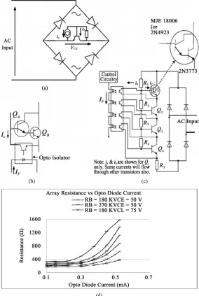
A conceptual approach for changing the effective overall AC resistance of a power BJT array over a wide range is shown in Figure 2. Figure 2(a) shows the simplified concept of control of the transistor. Figure 2(b) indicates how an opto isolator can be used to control current
di-version in the power semiconductor. Figure 2(c) indi-cates how series connected infrared emitter diodes in an opto isolator can be used to control a series connected bipolar power transistor array with AC operational capa-bility. When the transistor array is used in 230 V AC applications such as in an AC voltage regulator, the in-stantaneous values could often vary up to a maximum of approximately 330 2 V for a range of input AC RMS voltages from 160V to 260V [25]. This high voltage re-quirement at high power loads suggests the use of multi-ple power semiconductors to share the loading.
For an n-element BJT array similar to the case of Fig-ure 2(c), it can be shown that,
1 x B Array b i nR R i
(1)
when
1 B; 2 B1 ; 3 B2 ;
B B B Bn
R R R
R R R R
n n n
RB (2)
where RArray is the approximate effective instantaneous
resistance at the AC input of the circuit in Figure 2(c), ib
is the instantaneous base current, ix is the amount of
base current diverted by the opto transistors and RBis the
resistance between collector and base of the nth transistor
[22]. For the case of the 4 element array in Figure 2(c),
4 1 x B Array b i R R i
(3)
and,
1 4B; 2 3B; 3 2B; 4 B
R R R
R R R R R (4)
Note that the base emitter voltage drops are neglected in these approximations.
Based on the simplified relationship in Equation (3), the resistance between the collector and the emitter can be easily controlled either by varying RB or suitably
changing ix. This in effect indicates that we need to
con-trol the ratio i ix b, which is defined as the base current
3.2. Limits and Boundaries of the Achievable AC Resistance
Due to Darlington pairs in Figure 2(c) a cutoff condition is reached when the compound VBE value for the
Dar-lington pair is approximately less than about 1.0 Volt. This occurs at a higher value of the opto transistor cur-rent and at that point the controllability of the array im-pedance diminishes. This is the case beyond the maxi-mum BCDR, where the base current of each of the tran-sistors is totally removed by the action of the optoisola-tors. Under this condition, the effective resistance of the array is not controlled by the transistors, except for the leakage effects. If the transistor leakage effects are ne-
glected and the conditions in Equation (2) are maintained, the effective maximum resistance of the array reaches the value given by the series combination of the resistors
RB1 to RBn,
max 2B 3B 4B B
CE B
R R R R
R R
n
(5)
At the other extreme, when the current through the input diodes of the optoisolators is zero (the case of minimum BCDR), the effective resistance of the array reduces to nRB . In between these two limits the
overall resistance of the array, RCE, can be controlled by
varying the current through the series connected diodes.
(b) (c)
[image:4.595.156.440.258.681.2](d)
From Equation (5) the maximum value of effective re-sistance for an array of 4 elements is approximately 2.1
RB,neglecting the effects of leakage currents in
transis-tors. Equation (3) indicates that the minimum resistance for the array is approximately 4RB/β. This clearly
indi-cates a wide range of ideal performance possible within the boundaries. If the array is to work as a high voltage capable switching element, the value of RB can be set to a
suitable value for the designer to get the overall result of 4RB/β to reach the lowest necessary, based on the circuit
components. For a 4-element array the ratio of off-im- pedance/on-impedance is around β/1.9 and for a well configured Darlington pair this can be in the range of 3 orders.
Figure 2(d) depicts a typical example of the variation of the effective resistance versus control input IF
(opto-diode current)for RB values of 270 kΩ and 180 kΩ for a
four element array (as in Figure 2(c)) capable of 100W dissipation. It is clear that the lowest value reaches the theoretical value expected from 4RB/β. As indicated in Figure 2(d) for the case of 50 V AC input with RB = 270
kΩ, the array reaches a maximum at higher values of IF
as per theoretical predictions and SPICE simulations. However the maximum value is significantly lower than the expected due to leakage effects.
Also the graphs indicate the dependence of the effec-tive resistance on the AC line voltage, due to device nonlinearities and the dependence of β on the instanta-neous collector current over the AC cycle. Another prac-tical situation is that the transistors could have non iden-tical β values. However it is easy to compensate for this variation by slightly adjusting the RB values deviating
from the relationship in Equation (2).
4. Application Examples
4.1. Design of an AC Regulator Based on the Technique
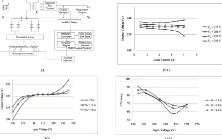
Figure 3(a) indicates the basic approach where the trans-former T1 allows the boost or buck operation. If you con-sider that the transformer is an ideal one, where the series winding has N times the turns as in the primary winding which is in series with the power semiconductor array placed across the bridge points of the full wave rectifier.
Under this arrangement, the following approximate relationship holds true, for any general load connected at the output.
1
2out in array L
V V N R N I (6)
where VOut and Vin are the output and input voltages
and IL is the load current in vectors respectively.
Figure 3(b) indicates the phasor diagrams for the case
where the input voltage (Vin ) is less than the required
regulated output (Vout ). In this example we consider the load current is lagging the input voltage by an angle Φ. Based on the relationship in Equation (6), and assuming that the impedance of the transistor array is purely resis-tive, and the transformer is ideal with no leakage induct-ances or resistinduct-ances, the control circuits could regulate the output voltage, by maintaining the regulated Vout
within the arc of the circle with a radius of Vout in the region where the tangential points of the worst case phase angles of the load falls within ±Φmax. Beyond these
limits of the tangential points T and T’ of the phasor
dia-gram, regulation is not possible, for a given turns ratio N. Few interesting and practically useful observation are that,
1) If the load is purely resistive, the regulated output voltage will be in phase with the input voltage;
2) For a given input voltage if the transformer is con-figured to have the case of Vout Vin
1N
, dissipationin the array is minimum;
3) Condition 2) above suggests having multiple taps in the transformer, to have the best efficiency under wide range of input voltage fluctuations;
4) When the transformer turns ratio increases, the al-lowable phase angle of the load decreases.
Figure 3(c) indicates the case of phasor diagram, where the input voltage is higher than the required regu-lated output voltage. In this situation, by creating a higher voltage across the array, and practically reversing the voltage at the primary winding, the regulation is achieved. In case the load is purely resistive, as expected the regulated output will be in phase with the input volt-age. Also in this situation, when the input voltage rises above the required regulated output value, it is possible to reverse the connections of the primary winding, so that the dissipation across the array is reduced. In Fig-ures 3(b) and 3(c) the arc included within T and T’
indi-cates the limits of the reactive component of the load to achieve regulation, assuming that the transformer is con-sidered ideal.
As shown in the phasor diagrams the technique is useful in situations with non resistive loads as well, while regulating the output for both voltage sags and surges with out any transformer configuration changes.
(a)
[image:6.595.113.492.78.361.2](b) (c)
Figure 3. BJT array based AC regulator and phasor diagrams. (a) Basic concept; (b)Phasor diagram when input voltage is less than the regulated output; (c) Phasor diagram when input voltage is higher than the regulated output.
L1
N1
T1
L
N
(a) (b1)
(b2) (b3)
[image:6.595.77.524.409.690.2]For RMS output voltage control, the effective resis-tance of the array is varied depending on the load and the input voltage. RMS control circuit compares the actual AC output sample, converted to a DC value using an RMS-DC converter IC, with a reference DC voltage. Current injection circuit adjusts the current injected into the series connected input diodes of the opto isolator, based on the output of the RMS control circuits. This effectively controls the value of Rarray in such a way that
the loop keeps the output RMS value regulated at a pre-set value such as 230 V, for a wide range of input volt-ages.
Figures 4(b1) to 4(b3) indicate the measured per-formance of an AVR prototype of output capacity of 1kVA based on Darlington pairs of 2N3773 and 2N4923 [17]. Load regulation graph in Figure 4(b1) indicates that the prototype regulates around 230 ± 6% V AC within an input voltage range of 170 V to over 250 V. The line regulation graph in Figure 4(b2) indicates that the technique is usable almost up to 160 V, however needs adjusting the lowest possible resistance of the ar-ray.
As per graph of Figure 4(b3) we see that the effi-ciency keeps dropping as the input voltage keeps in-creasing towards the nominal regulated value of 230 V. In the particular prototype tested [17], we have used a transformer with a turns ratio (N) of 70/160, where the array is expected to have the lowest resistance, at a worst case of input voltage of 160 V rms. If the input voltage reaches 230 V rms, the primary winding should have zero value so that the correction applied at the secondary side is zero. This indicates that the quantity
should be equal to
2
Array L
N R I
230 70 160
V, for the case of a pure resistive load. Similarly if the input voltage goes towards a surge situation with over 230 V rms value, this quantity should be further increased, to generate a nega-tive correction at the secondary winding.In this prototype where the efficiency is optimized around 160 V, as the input voltage increases the effi-ciency drops. However the overall performance is com-parable with a similar capacity ferro-resonant version. As discussed in a previous paragraph, by using multiple taps and reversing taps under surge voltage conditions at the input overall efficiency could be improved.
This gapless transformer based technique can be en-hanced with a digital control subsystem to minimize the harmonics at the output. By suitable control circuitry, transformer tap changes can also be incorporated to fur-ther enhance the overall efficiency, recognizing the fact that the technique has a higher efficiency at the worst case sags, where only a minimum resistance value of the array is required as per Equation (6).
4.2. Electronic AC Load
Another useful application of the technique is in an tronic AC load. The design approach for an AC elec-tronic load with processor control is indicated in [23-25]. A discussion on this is beyond the scope of this paper.
5. Processor Based Approach for
Linearizing of the Array Resistance
Given the non-linear behaviour of the transistor array as per Figure 2(d), the instantaneous current in the array will be nonlinear under general conditions, and will de-pend on the instantaneous AC line voltage as well as the dependency of the gain of transistor on its collector cur-rent. In order to control the non linearity of the value of
RArray which is equivalent to ( )
( )
Array rms Array rms
V
I , collector current
in the opto transistors based on the following relationship could be controlled [27].
' p F C F I I K I
(7) K, IF' and p are the parameters for opto isolator pairs
[27].
From the basic transistor parameter relationships and assuming that all transistors are identical,
e qVBE kT
Array S
I I (8)
where q is the electron charge, k is the Boltzmann con-stant and T is theabsolute temperature of the transistor junction. Is is the saturation current for the identical
tran-sistors Q1 to Q4 in Figure 2(c).
By substituting the relationships in Equation (7) and (8) in Equation (3),
' 4 1 e BE p F F B CE qV kT S I K I R R I (9)
With suitable mathematical manipulations [23], we can also arrive at the following relationship for voltage across the array (VCE) and the opto-diode forward current
(IF) for a given RCE value, neglecting the vBE compared to
the instantaneous values of vCE.
'ln ln B CE
CE F p
CE B F
K n R R
V p I
R n R I
(10)
arrangement in Figure 2(c), curve fitting techniques can be used to obtain the logarithmic relationships for volt-age across the array (VCE) and the current fed through the
photo diodes (IF) of the opto isolator for each value of
expected array resistance. Implementation of this is shown in Figure 5 depicting the hardware block diagram and the flow chart applicable. By plotting these curves from the experimental results (which tallies with the SPICE simulation results) together with a straight line fit, it could be easily seen that a reasonably accurate values for m and c values for a straight line approximation can be obtained. Two selected examples from [25] are shown for array resistances of 500 Ω and 50 Ω in Figure 6. From these graphs, one can see that the relationship is very close to a straight line fit, with matching R2 values
close to 1.
(a)
[image:8.595.308.540.76.429.2](b)
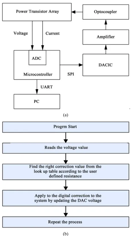
Figure 5. Approach to digital control of the harmonics at the output. (a) Processor and the control; (b) Flow chart.
(a)
(b)
Figure 6. Graphs of Logn (VCE) versus Logn (IF) for two dif-ferent RCEvalues together with straight line fit in each case (a) For RCE = 500 Ω; (b)For RCE = 50 Ω.
Given these relationships for a particular case of a transistor array, the values of m and c can be fed into the digital control algorithm, in an overall arrangement as in
Figure 5(a). A look up table can store the experimental values for the particular array, and then derive the ap-proximate values m and c suitable for each case of a straight line fit.
The above discussion leads towards the digital control approach to solve the linearity issue of the array, by con-trolling the two parameters m and c indicated above. Us-ing a digital control algorithm, injected opto diode cur-rent can be controlled to adjust the instantaneous curcur-rent through the array, by taking relatively larger number of samples of the AC voltage waveform via sampling. Overall effect of the processor based system is to control the opto diode current to achieve the expected impedance, based on the behaviour of the array as per Figure 2(c)
[image:8.595.58.287.285.695.2]program calculates the required opto diode current (out-put from the DAC) over each sampling period within the 50 or 60 Hz AC cycle. More details are available in [25] and a related US patent application.
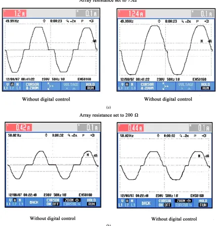
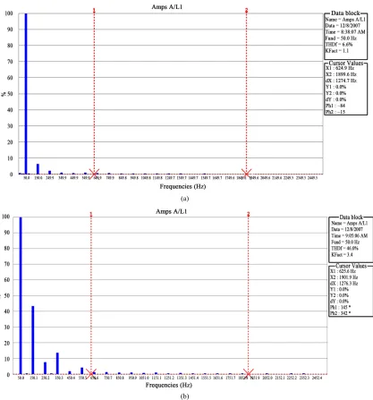
Figure 7 compares the array performance with and without digital control at different resistance settings. It is clear from these oscillographs forms that the digital control technique reduces the harmonics in the waveform. These results were obtained in an electronic AC load capable of 150 VA capacity, based on an 8 bit Zilog Z8 Encore processor [25]. Figure 8 indicates the fast Fou-rier transforms (FFT) of the current waveform at 1.3 A
with and without the digital controller. This FFT plots indicates that the technique reduces the 3rd, 5th , 7th and
9th harmonic etc by significant amounts, proving that the
algorithmic approaches used is clearly suitable. More information is available in [23].
Overall achievements in this work are:
1) A versatile AC impedance control technique which can be used in applications such as AVRs and power conditioners;
2) A new digital control technique where additional digital waveform control can be added to the system to minimize harmonics in the current waveforms.
(a)
(b)
(a)
[image:10.595.91.508.75.522.2](b)
Figure 8. Comparison of the FFT of the current waveform at 1.3 A (a) with digital control; (b) without digital control.
7. Conclusions
The concept of using a series transistor array with opto isolator based isolation can be used in several AC power control applications suitable for low power and single phase requirements. Paper provides a general analysis of the array, and the design details of a 1 KVA capacity AVR prototype, which can be extended into other power levels. One secondary advantage of the technique is its ability to incorporate digital control algorithms to mini-mize harmonics due to the non linear nature of the power semiconductor array. Given these details, the technique could be used to develop AVRs with performance far superior to ferro-resonant versions and other slow
re-sponding transformer tap changers etc.
In addition, this technique has the potential to combine with common AVR techniques such as transformer tap changers etc for higher overall efficiency. Another pos-sible application is in electronic AC loads with harmonic control.
8. References
[1] G. T. Heydt, “Electric Power Quality: A Tutorial Intro-duction,”IEEE Computer Applications in Power, Vol. 11, No. 1, 1998, pp. 15-19.
and Duration of Voltage Sags and Surges at Industrial Sites,” IEEE Transactions on Industry Applications, Vol. 34, No. 5, 1998, pp. 904-910.
doi:10.1109/28.720428
[3] K. M. Michaels, “Sensible Approaches to Diagnosing Power Quality Problems,” IEEE Transactions on Industry Applications, Vol. 33, No. 4, 1997, pp. 1124-1130. [4] A. Domijan, J. T. Heydt, A. P. S. Meliopoulos, M. S. S.
Venkata and S. West, “Directions of Research on Electric Power Quality,” IEEE Transactions on Power Delivery, Vol. 8, No. 1, 1993, pp. 429-436.
[5] R. Ellis and B. Guidry, “Power Quality Concerns and Solutions,” IEEE Industry Applications Magazine, Vol. 11, No. 6, 2005, pp. 20-24.
[6] W. E. Kazibwe and H. M. Sendaula, “Expert System Targets Power Quality Issues,” IEEE Computer Applica-tions in Power, Vol. 5, No. 2, 1992, pp. 29-33.
[7] N. Kularatna, “Worst Case Power Quality Environments and Design of Power Electronics Products: Experiences of a Design Team in a Developing Country,” Proceedings of Power Systems World—2000 Conference (Power Quality’2000), USA, pp. 109-116.
[8] Magtech Voltage Booster, Magtech.
http://www.magtech.no/www.
[9] G. Evans, “Power Quality Source Book,” Intertec Inter-national, Ventura, 1991.
[10] J. W. Clarke, “AC Power Conditioners,” Academic Press, Cambridge, 1990.
[11] C. Chen and D. Divan, “Simple Topologies for Single Phase AC Line Conditioning,” IEEE Transactions on In-dustry Applications, Vol. 30, No. 2, 1994, pp. 406-412.
doi:10.1109/28.287516
[12] D. Jang and G. Choe, “Step-up/down Ac Voltage Regu-lator Using Transformer with Tap Changer and PWM AC Chopper,” IEEE Transactions on Industrial Electronics, Vol. 45, No. 6, 1998, pp. 905-911.
[13] Y. S. Lee, D. K. W. Cheng, and Y. C. Cheng, “Design of a Novel Ac Regulator,” IEEE Transactions on Industrial Electronics, Vol. 38, No. 2, 1991, pp. 89-94.
doi:10.1109/41.88900
[14] J. C. Bowers, S. J. Garret, H. A. NienHaus and J. L. Brooks, “A Solid State Transformer,” IEEE Power Elec-tronics Specialists Conference, Atlanta, 16-20 June 1980, pp. 253-264.
[15] M. T. Tsai, “Analysis and Design of a Cost-Effective Series Connected AC Voltage Regulator,” IEE Proceed-ings of Electric Power Applications, Vol. 151, No. 1, 2004, pp. 107-115.
[16] M. T. Tsai, “Design of a Compact Series-Connected AC Voltage Regulator with an Improved Control Algorithm,”
IEEE Transactions on Industrial Electronics, Vol. 51, No. 4, 2004, pp. 933-936.
[17] A. D. V. N. Kularatna, “Low Cost, Light Weight AC Regulator Employing Bipolar Power Transistors,” Pro-ceedings of the 21st International Power Quality Con-ference, Philadelphia, 24 October 1990, pp. 67-76. [18] A. D. V. N. Kularatna, “Techniques Based on Bipolar
Power Transistor Arrays for Regulation of Ac Line Volt-age,” Proceedings of the 5th Annual European Confer-ence on Power Electronics and Applications, Brighton, 13-16 September 1993, pp. 96-100.
[19] A. D. V. N. Kularatna and S. D. Godakumbura, “Use of Spice Simulation for Predicting the Harmonic Capability of an Ac Regulator Technique Based on a Bipolar Power Transistor Array,” Proceedings of the 5th International Conference on Power Electronics and Variable Speed Drives, London, 26-28 October 1994, pp. 157-162.
doi:10.1049/cp:19940957
[20] A. D. V. N. Kularatna and S. D. Godakumbura, “Use of Voltage Dip and up Simulator for Testing the Transient Behaviour of a Bipolar Power Transistor Array Based Ac Line Voltage Regulator,” Proceedings of European Con-ference on Power and Applications, Vol. 3, pp. 3.298- 3.303.
[21] C. R. Selvakumar, “Negative Feedback High Efficiency Ac Voltage Regulator,” IEEE Transactions on Industrial Electronics and Control Instrumentation, Vol. IECI-28, No. 1, 1981, pp. 24-27. doi:10.1109/TIECI.1981.351019
[22] “A Linear technique for Ac Voltage Regulation Using an Ordinary Transformer and Power Semiconductors,” Sri Lanka Patent No. 10028, 1990.
[23] N. Kularatna and P. Cho, “A Power Sharing Series Power BJT Array with Isolated Low Voltage Control for AC Power Control Applications,” 32nd Annual Conference on IEEE Industrial Electronics, Paris, 6-10 November 2006, pp. 1715-1720. doi:10.1109/IECON.2006.347430
[24] N. Kularatna and P. Cho, “Design Approach to an AC Electronic Load Base Don Generalized Series Power Transistor Array,” CD-ROM, Session PQT 17, Power Quality Conference, Long beach, October 2006.
[25] C. Jinadasa, “High Power Linear Electronic AC Load for Testing UPS Systems.” Master’s Thesis, The University of Waikato, Hamilton, 2007.
[26] N. Kularatna, “Power Electronics Design Handbook-Low Voltage Components and Applications, Chapter 6,” But-terworth, Oxford, 1998.
[27] K. Goulet, “Automation Equipment of the 90s-Power Conditioning Equipment of the 60s,” Proceedings of the Power Quality, USA, 1990, pp. 64-77.