DESIGN OF A LOW POWER FLASH ADC USING THRESHOLD INVERTER QUANTIZATION
TECHNIQUE IN 90NM TECHNOLOGY
*,1
Shailendra Prakash
1
M.Tech Scholar, Dept. of VLSI Design, F.O.T. Uttarakhand Technical University, Dehradun
2Astt. Prof. (H.O.D.), Dept. of VLSI Design, F.O.T. Uttarakhand Technical University, Dehradun
ARTICLE INFO ABSTRACT
All the signals are analog in nature. An analog to digital converter plays an important and essential role for system
world and the digital logical
more important issues as the channel length of the MOSFET shrinks so below levels. For improvement of power and s
comparator. This paper presents a design of 4 applications using Threshold Inverter Quantization inverter
requirement of resister or capacitor ladder circuit. Threshold inverter quantization provides high speed, low power, and smaller area. TIQ also eliminates the requirement o
voltage comparator that are inherently more compound and slower than digital inverters. TIQ based flash ADC also eliminates the need of reference voltages, which require a resister ladder circuit. In the TIQ based flash ADC t
voltage is used as a reference voltage for comparing the input voltage and produce the thermometer code. An efficient thermometer to binary converter has been designed using tran
on 2*1 multiplexer. Power consumption reduced as per accordance to threshold voltage and for high speed transistor size must kept small. The TIQ based flash ADC requires 2
the number of bits or resolution. To
should not be deviated too much and keep W capacitance.
Copyright©2017, Shailendra Prakash and Dr. Vishal Ramola
permits unrestricted use, distribution, and reproduction in any medium, provided the original work is properly cited.
INTRODUCTION
Analog to digital converter plays important role in design of mixed signal, system on chip and signal processing applications. There are various types of ADCs. Depending on ADC’s speed ADC’s are classified in three categories; (Shailendra Prakash and Vishal Ramola, 2017
serial ADC, (Ranam Sireesha and Abhishek Kumar Medium speed ADC, and (Pradeep Kumar, 2011
ADC. The serial ADC operates at lower conversion speed but having high resolution. High speed ADC operates at high speed. Now depending upon various topologies the ADCs are classified as; (Shailendra Prakash and Vishal Ramola
Flash ADC (Ranam Sireesha and Abhishek Kumar Sigma delta ADC (Pradeep Kumar, Amit Kolhe
*Corresponding author: Shailendra Prakash
M.Tech Scholar, Dept. of VLSI Design, F.O.T. Uttarakhand Technical University, Dehradun
ISSN: 0975-833X
Article History:
Received 09th February, 2017
Received in revised form 21st March, 2017 Accepted 14th April, 2017
Published online 23rd May,2017
Citation: Shailendra Prakash and Dr. Vishal Ramola.
technology”, International Journal of Current Research
Key words:
Analog-to-digital converter, Flash ADC,
Threshold Inverter Quantization, Comparator, 2*1 multiplexer, Low Power, Encoder.
RESEARCH ARTICLE
DESIGN OF A LOW POWER FLASH ADC USING THRESHOLD INVERTER QUANTIZATION
TECHNIQUE IN 90NM TECHNOLOGY
Shailendra Prakash and
2Dr. Vishal Ramola
VLSI Design, F.O.T. Uttarakhand Technical University, Dehradun
Astt. Prof. (H.O.D.), Dept. of VLSI Design, F.O.T. Uttarakhand Technical University, Dehradun
ABSTRACT
All the signals are analog in nature. An analog to digital converter plays an important and essential role for system-on-chip (SOC) applications because it bridges the gap between the analog physical world and the digital logical world. Now a days low power and low voltage requirements becoming more important issues as the channel length of the MOSFET shrinks so below levels. For improvement of power and speed in an analog to digital converter major building block is a comparator. This paper presents a design of 4-bit low power flash ADC for system applications using Threshold Inverter Quantization (TIQ) comparators. The technique threshold inverter quantization uses two cascaded CMOS inverters as a comparator
requirement of resister or capacitor ladder circuit. Threshold inverter quantization provides high speed, low power, and smaller area. TIQ also eliminates the requirement o
voltage comparator that are inherently more compound and slower than digital inverters. TIQ based flash ADC also eliminates the need of reference voltages, which require a resister ladder circuit. In the TIQ based flash ADC the reference voltage is internally generated by the circuit that is threshold voltage is used as a reference voltage for comparing the input voltage and produce the thermometer code. An efficient thermometer to binary converter has been designed using tran
on 2*1 multiplexer. Power consumption reduced as per accordance to threshold voltage and for high speed transistor size must kept small. The TIQ based flash ADC requires 2
the number of bits or resolution. To reduce the power consumption of the design, the threshold voltage should not be deviated too much and keep WP/Wn < 1 to reduce power consumption and paracitic capacitance.
Shailendra Prakash and Dr. Vishal Ramola.This is an open access article distributed under the Creative Commons Att
use, distribution, and reproduction in any medium, provided the original work is properly cited.
Analog to digital converter plays important role in design of mixed signal, system on chip and signal processing applications. There are various types of ADCs. Depending on ADC’s speed ADC’s are classified in three categories; , 2017). Low speed Ranam Sireesha and Abhishek Kumar, 2015). , 2011). High speed The serial ADC operates at lower conversion speed but having high resolution. High speed ADC operates at high speed. Now depending upon various topologies the ADCs are Shailendra Prakash and Vishal Ramola, 2017). and Abhishek Kumar, 2015). Pradeep Kumar, Amit Kolhe, 2011).
M.Tech Scholar, Dept. of VLSI Design, F.O.T. Uttarakhand Technical
Successive approximation ADC. The speed o
by the solid state technology used to implement the converter. There are three types of solid state technologies available for high speed ADC implementation; CMOS technology, the bipolar technology, and the gallium arsenide (GaAs) technology. The CMOS technology allows a high density of logic functions on a chip and also CMOS technology is used technology is widely used technology to be implemented in VLSI. The GaAs technology is fastest of the three technology and the CMOS technology is t
The ultrafast ADCs are implemented with Flash type using GaAs technology, but the GaAs technology is not compatible with Si CMOS technology, by which it is difficult to realize the SOC Applications. The bipolar technology al
operation and it is compatible with CMOS technology but it needed more processing steps and higher cost than the standard CMOS technology. Due to all these reasons here a new technique i.e. TIQ comparator is introduced here which provide higher speed and compatible with current CMOS International Journal of Current Research
Vol. 9, Issue, 05, pp.50891-50895, May, 2017
INTERNATIONAL
OF CURRENT RESEARCH
Shailendra Prakash and Dr. Vishal Ramola. 2017. “Design of a low power flash ADC using threshold inverter quantization technique in 90nm
International Journal of Current Research, 9, (05), 50891-50895.
Available online at http://www.journalcra.com
z
DESIGN OF A LOW POWER FLASH ADC USING THRESHOLD INVERTER QUANTIZATION
VLSI Design, F.O.T. Uttarakhand Technical University, Dehradun
Astt. Prof. (H.O.D.), Dept. of VLSI Design, F.O.T. Uttarakhand Technical University, Dehradun
All the signals are analog in nature. An analog to digital converter plays an important and essential it bridges the gap between the analog physical world. Now a days low power and low voltage requirements becoming more important issues as the channel length of the MOSFET shrinks so below levels. For peed in an analog to digital converter major building block is a bit low power flash ADC for system-on-chip (TIQ) comparators. The technique threshold quantization uses two cascaded CMOS inverters as a comparator, that eliminates the requirement of resister or capacitor ladder circuit. Threshold inverter quantization provides high speed, low power, and smaller area. TIQ also eliminates the requirement of high gain differential input voltage comparator that are inherently more compound and slower than digital inverters. TIQ based flash ADC also eliminates the need of reference voltages, which require a resister ladder circuit. In the he reference voltage is internally generated by the circuit that is threshold voltage is used as a reference voltage for comparing the input voltage and produce the thermometer code. An efficient thermometer to binary converter has been designed using transmission gate based on 2*1 multiplexer. Power consumption reduced as per accordance to threshold voltage and for high speed transistor size must kept small. The TIQ based flash ADC requires 2n-1 comparators, where n is reduce the power consumption of the design, the threshold voltage 1 to reduce power consumption and paracitic
article distributed under the Creative Commons Attribution License, which
Successive approximation ADC. The speed of ADC is affected by the solid state technology used to implement the converter. There are three types of solid state technologies available for high speed ADC implementation; CMOS technology, the bipolar technology, and the gallium arsenide (GaAs) ogy. The CMOS technology allows a high density of logic functions on a chip and also CMOS technology is used technology is widely used technology to be implemented in VLSI. The GaAs technology is fastest of the three technology and the CMOS technology is the slowest of three technology. The ultrafast ADCs are implemented with Flash type using GaAs technology, but the GaAs technology is not compatible with Si CMOS technology, by which it is difficult to realize the SOC Applications. The bipolar technology allows faster operation and it is compatible with CMOS technology but it needed more processing steps and higher cost than the standard CMOS technology. Due to all these reasons here a new technique i.e. TIQ comparator is introduced here which speed and compatible with current CMOS
INTERNATIONAL JOURNAL OF CURRENT RESEARCH
technology. The main advantage of TIQ techniques is it has simpler speed and eliminates the resister ladder circuit requirement as in conventional ADC which increases its speed and decreases area.
Flash ADC
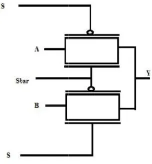
The Flash ADC is known as fastest ADC among all the ADC. IT is also known as parallel type ADC because of its parallel architecture. It converts data parallely simultaneously so it has high speed of conversion. The flash ADC comprises of two basic building blocks i.e. comparator and encoder. Comparator block compares the input voltage with reference voltage and generates thermometer code. The encoder block converts the thermometer code into digital output values. The flash ADC requires 2n-1 different size comparators for generation of thermocode. Here ‘n’ is the number of bits or resolution. The size of transistor is varied as length or width of transistor is change. One of the most important feature of flash ADC is high power consumption and large chip area
[image:2.595.314.553.92.218.2]dissipation increases with the speed and resolution i.e. higher power is consumed at higher speeds. But it is desirable that to design high speed ADC with less power dissipation.
Fig. 1. Block Diagram of TIQ Flash ADC
TIQ Comparator
A comparator is the heart of an ADC circuit. The main work of a comparator is to compare input voltage with reference voltage and generate thermocode. The TIQ comparator is basic CMOS inverter which comprises of two inverter stage, in which first stage works as a comparator and the second inverter stage works as gain booster, which increases the voltage gain of comparator and manages the propagation delay in balance. The second stage is exactly same as first stage to maintain the same DC threshold level and to
in balance for voltage variations of high frequency inputs. A TIQ comparator is different from differential comparator only due to its reference voltage. The differential comparator utilizes the external reference voltage ‘Vr’ using resistor ladder circuit, however the TIQ comparator sets reference voltage internally on the basis of transistor size.
TIQ based flash ADC
A conventional ADC consists of 2n resisters in series to generate the reference voltage which requires larg
and high power consumption. But the TIQ based flash ADC
50892 Shailendra Prakash and Dr. Vishal Ramola,
technology. The main advantage of TIQ techniques is it has simpler speed and eliminates the resister ladder circuit requirement as in conventional ADC which increases its speed
The Flash ADC is known as fastest ADC among all the ADC. IT is also known as parallel type ADC because of its parallel architecture. It converts data parallely simultaneously so it has high speed of conversion. The flash ADC comprises of two blocks i.e. comparator and encoder. Comparator block compares the input voltage with reference voltage and generates thermometer code. The encoder block converts the thermometer code into digital output values. The flash ADC omparators for generation of thermocode. Here ‘n’ is the number of bits or resolution. The size of transistor is varied as length or width of transistor is change. One of the most important feature of flash ADC is high power consumption and large chip area. The power dissipation increases with the speed and resolution i.e. higher power is consumed at higher speeds. But it is desirable that to design high speed ADC with less power dissipation.
Block Diagram of TIQ Flash ADC
mparator is the heart of an ADC circuit. The main work of a comparator is to compare input voltage with reference voltage and generate thermocode. The TIQ comparator is basic CMOS inverter which comprises of two inverter stage, in s a comparator and the second inverter stage works as gain booster, which increases the voltage gain of comparator and manages the propagation delay in balance. The second stage is exactly same as first stage to maintain the same DC threshold level and to keep the linearity in balance for voltage variations of high frequency inputs. A TIQ comparator is different from differential comparator only due to its reference voltage. The differential comparator ’ using resistor ladder circuit, however the TIQ comparator sets reference voltage
resisters in series to generate the reference voltage which requires large chip area and high power consumption. But the TIQ based flash ADC
[image:2.595.59.265.330.496.2]generates reference voltage internally i.e. chip area reduced and also it require low power consumption.
Fig. 2. TIQ Schematic & VTC
In the TIQ based ADC all the comparators are of d
where as in conventional ADC all the comparators are of identical size. Advantages of TIQ based flash ADC are;
Simple comparator design.
No need of external reference voltage.
Faster voltage comparison speed.
Does not require switches,
capacitors for the voltage comparison. No need of resister ladder circuit. Suitable for system-on-chip applications.
Suitable for CMOS technology.
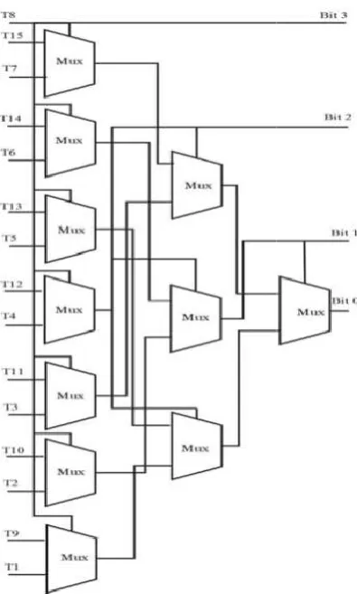
Encoder
An encoder is a device that converts infor
format to another for purpose of standardization, speed or compressions. A simple encoder assigns a binary code to an active input line. For an ADC an encoder is a circuit that converts the thermometer code into the binary code. Thermometer to binary encoder can be implemented by various approaches e.g. Fat tree, ROM type, logic based, multiplexer based. Among various types of encoders multiplexer based encoder requires less hardware and shorter critical path. A multiplexer is the circuit that gives single output as per accordance to multiple inputs. Here the 2*1 multiplexer based encoder is used. The multiplexers used are designed using transmission gates for better accuracy. A 2*1 multiplexer is the circuit which having 2 input lines and o
single select line.
Fig. 3. Multiplexer Schematic
, Design of a low power flash ADC using threshold inverter quantization technique in 90nm technology
generates reference voltage internally i.e. chip area reduced and also it require low power consumption.
TIQ Schematic & VTC
In the TIQ based ADC all the comparators are of different size where as in conventional ADC all the comparators are of identical size. Advantages of TIQ based flash ADC are;
Simple comparator design.
No need of external reference voltage. Faster voltage comparison speed.
Does not require switches, clock signals or coupling capacitors for the voltage comparison.
No need of resister ladder circuit. chip applications. Suitable for CMOS technology.
An encoder is a device that converts information from one format to another for purpose of standardization, speed or compressions. A simple encoder assigns a binary code to an active input line. For an ADC an encoder is a circuit that converts the thermometer code into the binary code. to binary encoder can be implemented by various approaches e.g. Fat tree, ROM type, logic based, multiplexer based. Among various types of encoders multiplexer based encoder requires less hardware and shorter critical path. A at gives single output as per accordance to multiple inputs. Here the 2*1 multiplexer based encoder is used. The multiplexers used are designed using transmission gates for better accuracy. A 2*1 multiplexer is the circuit which having 2 input lines and one output line with
Multiplexer Schematic
[image:2.595.361.514.602.767.2]Fig. 4. 2*1 Multiplexer Based Encoder
Proposed Work
In our work we are designing a low power Analog to Digital converter which operates at low voltage. The implementation is carried out on Symica DE tool. The process technology used is 90nm. For n-bit Flash ADC,2n-1 comparators are required. Here 04-bit ADC is designed for which 15
designed. In this design we take constant
n-and constant p-mos length, with varying the width of p calculate the switching voltage and can be mathematically calculated as;
…………(01) Where; Vdd = supply voltage.
Vtp = pmos threshold voltage. Vtn = nmos threshold voltage. Kp = (W/L)p . µp . Cox. Kn = (W/L)n. µn . Cox. µp = mobility of holes. µn = mobility of electrons. Wp = width of pmos. Wn = width of nmos. Cox = gate oxide thickness.
Switching voltage is calculated by equation (01) with varying pmos width and maintaining transistor length. All the calculated switching voltages are noted in table [01] (from ref.02).
50893 International Journal of Current Research,
2*1 Multiplexer Based Encoder
In our work we are designing a low power Analog to Digital converter which operates at low voltage. The implementation is carried out on Symica DE tool. The process technology used 1 comparators are required. is designed for which 15-comparators are -mos length-width mos length, with varying the width of p-mos to calculate the switching voltage and can be mathematically
[image:3.595.62.260.50.379.2]Switching voltage is calculated by equation (01) with varying pmos width and maintaining transistor length. All the calculated switching voltages are noted in table [01] (from
Table 1. Switching Voltages for Different PMOS width
Wn(µm) Wp(µm)
0.120 0.120
0.120 0.215
0.120 0.285
0.120 0.385
0.120 0.685
0.120 0.920
0.120 1.225
0.120 1.640
0.120 2.195
0.120 2.935
0.120 3.925
0.120 7.015
0.120 12.545
0.120 22.435
[image:3.595.329.539.62.788.2]0.120 30
[image:3.595.39.208.552.727.2]Fig. 5. TIQ Shematic
Fig. 6. VTC of TIQ Comparator
Fig. 7. Parametric Analysis of TIQ Comparator
International Journal of Current Research, Vol. 9, Issue, 05, pp.50891-50895, May, 2017
Switching Voltages for Different PMOS width
(µm) Vs(v)
0.120 0.336
0.215 0.358
0.285 0.371
0.385 0.384
0.685 0.410
0.920 0.421
1.225 0.430
1.640 0.442
2.195 0.455
2.935 0.467
3.925 0.473
7.015 0.497
12.545 0.513
22.435 0.530
30 0.542
TIQ Shematic
VTC of TIQ Comparator
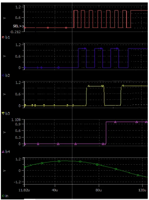
Fig. 8. Multiplexer Schematic
Fig. 9. Multiplexer Output
Fig. 10. 04-Bit Flash ADC
50894 Shailendra Prakash and Dr. Vishal Ramola
Schematic
Fig. 11. Output of 04
The comparator compares the voltage with internally generated reference voltage. Comparator gives output as logic high (i.e. 1) when input voltage (Vin) is greater than the reference voltage and the comparator gives o
when input voltage (Vin) is less than the reference voltage. An input sine wave with frequency
been applied to 15 different TIQ.
Conclusion
Here a simple and fast 04-bit flash ADC architecture has implemented with new comparator style that uses two cascaded inverters i.e. known as Threshold Inverter Quantization (TIQ) and 2*1 multiplexer logic based encoder. Flash ADC provides higher data sampling rate and operates at low voltage and also low power consumption. This design is suitable for System-On-chip
simulations are carried out by Symica DE with 90nm process technology.
REFERENCES
“Design of Analog CMOS integrated circuits by Behzad Razavi, Tata Mcgraw hill, 1s
“Design of novel high speed dynamic comparator with low power Dissipation For High Speed ADCs” a thesis submitted by Prasun Bhattacharya, NIT, Rourkela, May 2011.
6-BIT CMOS FLASH ADC USING TIQ COMPARATOR IN 0.250μM TECHNOLOGY
Electronics, Communication &Instrumentation
Engineering Research and Development
Dr. Vishal Ramola, Design of a low power flash ADC using threshold inverter quantization technique in 90nm technology
Output of 04-Bit Flash ADC
The comparator compares the voltage with internally generated reference voltage. Comparator gives output as logic high (i.e. ) is greater than the reference voltage and the comparator gives output as logic low (i.e. 0) ) is less than the reference voltage. An input sine wave with frequency 5KHZ and amplitude 1v has been applied to 15 different TIQ.
bit flash ADC architecture has been implemented with new comparator style that uses two cascaded inverters i.e. known as Threshold Inverter Quantization (TIQ) and 2*1 multiplexer logic based encoder. Flash ADC provides higher data sampling rate and operates at ower consumption. This design is (SOC) applications. All the simulations are carried out by Symica DE with 90nm process
“Design of Analog CMOS integrated circuits by Behzad Razavi, Tata Mcgraw hill, 1st Edition, (2002).
“Design of novel high speed dynamic comparator with low power Dissipation For High Speed ADCs” a thesis submitted by Prasun Bhattacharya, NIT, Rourkela, May
BIT CMOS FLASH ADC USING TIQ COMPARATOR IN
0.250μM TECHNOLOGY International Journal of
Electronics, Communication &Instrumentation
Engineering Research and Development (IJECIERD)
[image:4.595.46.281.54.566.2]ISSN(P): 2249-684X; ISSN(E): 2249-7951 Vol. 5, Issue 3, Jun 2015, 27-36 © TJPRC Pvt. Ltd.
A Variable Threshold Voltage CMOS Comparator for Flash Analog to Digital Converter International Journal of Computer Applications (0975 – 8887) Volume 88 – No.7, February 2014.
Arunkumar. P. Chavan, Rekha. G, P. Narashimaraja “ Design of a 1.5-V, 4-bit Flash ADC using 90nm Technology”, International Journal of Engineering and Advanced Technology (IJEAT) ISSN: 2249 – 8958, Volume-2, Issue-2, December 2012.
Black. B., “Analog-to-Digital Converter Architectures and Choices for System Design”. Analog Dialogue, 33-8, 1999. Broekaert, T. P. E., Brar, B., J. P. A. van der Wagt, A. C. Seabaugh, F. J. Morris, T. S. Moise, E. A. Beam III, and G. A. Frazier. “A Monolithic 4-Bit 2-Gsps Resonant Tunneling Analog-to-Digital Converter”. IEEE Journal of Solid-State Circuits, 33(9):1342{1349, September 1998. Channakka Lakkannavar, Shrikanth K. Shirakol, Kalmeshwar
N. Hosur, “Design, Implementation and Analysis of Flash Adcarchitecture with Differential Amplifier as Comparator using Custom Design Approach” International Journal of Electronics Signals and Systems (IJESS) ISSN: 2231- 5969, Vol-1 Iss-3, 2012.
Channakka Lakkannavar, Shrikanth K. Shirakol, Kalmeshwar N. Hosur, “Design, Implementation and Analysis of Flash Adcarchitecture with Differential Amplifier as Comparator using Custom Design Approach” International Journal of Electronics Signals and Systems (IJESS) ISSN: 2231- 5969, Vol-1 Iss-3, 2012.
Chetan Vudadha, Goutham Makkena, M Venkata Swamy Nayudu, Sai Phaneendra P, Syed Ershad Ahmed,Sreehari Veeramachaneni, N Moorthy Muthukrishnan, M.B. Srinivas “Low-Power Self Reconfigurable Multiplexer Based Decoder for Adaptive Resolution Flash ADCs” 2012 25th International Conference on VLSI Design.
Choe, M., B. Song, and K. Bacrania. “An 8-b 100 MSample/s CMOS Pipelined Folding ADC”. IEEE Journal of Solid-State Circuits, 36(2):184{194, February 2001.
Daegyu Lee, Jincheol Yoo, and Kyusun Choi “Design Method and Automation of Comparator Generationfor Flash A/D
Converter” Department of Computer Science &
Engineering,The Pennsylvania State University, University Park, PA 16802.
Dalton, D., Spalding, G. J., Reyhani, H., T. Murphy, K. Deevy, M. Walsh, and P. Gri_n. “A 200-MSPS 6-bit Flash ADC in 0.6-_m CMOS”. IEEE Transactions on Circuits and System II, 45(11):1433{1444, November 1998.
Donovan, C. and Flynn, M. P. 2002. “A `Digital' 6-bit ADC in 0.25 _m CMOS. IEEE Journal of Solid-State Circuits”, 37(3):432{437, March 2002.
Fayomi, C. J. B., G.W. Roberts, and M. Sawan. “A 1-V 10-bit Rail-to-Rail Successive Approximation Analog-to-Digital Converter in Standard 0.18 _m CMOS Technology”. In IEEE International Symposium on Circuits and Systems, volume 1, pages 460{463, 2001.
Ila Gupta1, Neha Arora, Prof. B.P. Singh “Simulation and Analysis of 2:1 Multiplexer Circuits at 90nm Technology” International Journal of Modern Engineering Research (IJMER), Vol.1, Issue.2, pp-642-646 ISSN: 2249-6645.
Kalpana Chaudhary, R. B. Singh “Novel Approach to 3-Bit Flash ADC” IJSRD - International Journal for Scientific Research & Development| Vol. 2, Issue 03, 2014 | ISSN (online): 2321-0613.
Kalpana Chaudhary, R. B. Singh “Study of a 3-bit CMOS flash
ADC utilizing Threshold Inverter Quantization
technique”.IJSRD - International Journal for Scientific Research & Development| Vol. 2, Issue 03, 2014.
Kwok, P. T. F. and Luong. H. C. 2001. “Power Optimization
for Pipeline Analog-to-Digital Converter”. IEEE
Transactions on Circuits and System II, 46(5):549{553, May.
Liyaqat Nazir, Roohie Naaz Mir, Najeeb-ud-din Hakim “A 4 GS/s,1.8 V Multiplexer encoder based Flash ADC using TIQ Technique.” 2014 International Conference on Signal Processing and Integrated Networks.
Neha Prabhat, Amana Yadav “A Review of Low Power Flash ADC Using Different Comparator Styles & Design Techniques”.ISSN(Online): 9801ISSN (Print) : 2320-9798 International Journal of Innovative Research in Computer and Communication Engineering.
Oktay Aytar and Ali Tangel “Employing threshold inverter quantization (TIQ) technique in designing 9-Bit folding and interpolation CMOS analog-to-digital converters (ADC)”. Scientific Research and Essays Vol. 6(2), pp. 351-362, 18 January, 2011.DOI: 10.5897/SRE10.793 ISSN 1992-2248 ©2011.
Pradeep Kumar, Amit Kolhe, “Design and Implementation of LowPower 3-bit Flash ADC in 0.18μm CMOS,”
International Journal of Soft Computing and
Engineering(IJSCE), ISSN: 2231-2307, Volume-I,Issue-5, November 2011.
Prof. S.S. Khot, Dr. P. W. Wani, Dr M S Sutaone, Shubhang Tripathi “Design of a 45nm TIQ Comparator for High Speed and Low Power 4-Bit Flash ADC” 2010
Ranam Sireesha and Abhishek Kumar “Design of low power 0.8v Flash ADC using TIQ in 90nm Technology”2015 IEEE.
Sagar Mukherjee, Dipankar Saha, Posiba Mostafa, Sayan Chatterjee, C. K. Sarkar, "A 4-bit Asynchronous Binary Search ADC for Low Power, High Speed Applications, International Symposium on Electronic System Design, 2012.
Shailendra Prakash and Vishal Ramola “A Review of Low Power Flash ADC using Threshold Inverter Quantization Technique”wjert 2017,vol 3, issue 3, 104-114.
Sujeet Mishra and Balchand Nagar “ Design of a TIQ Comparator for High Speed and Low Power 4 bit Flash ADC” International Journal of Emerging Technologies in Computational and Applied Sciences (IJETCAS).
Sujeet Mishra and Balchand Nagar “DESIGN of a TIQ COMPARATOR for HIGH SPEED and LOW POWER 4 BIT FLASH ADC” Electronics & Communication Acropolis Instt. of Tech. & Research, Indore INDIA International Journal of Emerging Technologies in Computational and Applied Sciences (IJETCAS) 2013. The Institute of Electrical and Electronics Engineers, Inc.
(IEEE). IEEE Standard for “Teminology and Test Methods for Analog-to-Digital Converters”, 2001. IEEE Std 1241-2000.