DESIGN AND IMPLEMENTATION OF HIGH SPEED OPTIMIZED SDRAM CONTROLLER BASED
1
Komala, M.,
2Dr. Nataraj
1
Research Scho
2Prof & HOD,
3Associate Professor
ARTICLE INFO ABSTRACT
These days the requirement of memory is increasing day by day as it has become one of the integral part of the our day to day equipment’s that we use such as phones, computers, etc. the main
the popularity is its upgraded features like high speed of operation, easy to configure, very small in size and hence occupy negligible area, improved latency, and high performance. It has become possible due to advance controller that is used
to the SDRAM to perform at its best and provide outstanding features for the users. Hence it is very much necessary to design a controller for the SDRAM memory element to enhance its functionality. The pa
designed for high speed interface with PCI Bus that can handle huge amount of data and can be used for various storage related application such as BIG DATA, etc. Th
mainly comprised of some of the basic functionality like read, write operation, refresh, synchronization, etc. The design developed is implemented on FPGA operating on 200MHz clock frequency and coded using verilog lan
and Modelsim6.3 is used to work on the functional verification of the design.
Copyright©2016, Komala et al. This is an open access article distributed under the Creative Commons Att distribution, and reproduction in any medium, provided the original work is properly cited.
INTRODUCTION
All most all the electronic devices used these days make use of memory element to perform various operations. As we know the memories are used for data storage and need of large data storage is increasing every day. All the electronics equipment’s right starting from video games for kids of high resolution camera or even satellite are in need of memory as per the requirements. This increasing demand of memory for the devices has thrown challenges to the engineers to design something robust and reliable that can be used for
engineering. Not only is the usage of memory looked into the event but also the speed of operation is important. Various medical and aerospace electronic devices are used these days that need very efficient, high speed and large memory on boar for the application (Heitheckerand Ernst, 2005)
registers were used as a storage element for the devices as the requirements was small the registers were working very
*Corresponding author: Dr. Mallikarjunaswamy, S.
Associate Professor, Department of ECE, SJBIT, Bengaluru, India.
ISSN: 0975-833X
Article History:
Received 20th April, 2016
Received in revised form 29th May, 2016
Accepted 04th June, 2016
Published online 16th July,2016
Key words:
Xilinx, FPGA, SDRAM, Controller, double data rate, Read and Write operation, Throughput.
Citation: Komala, M., Dr. Nataraj, K. R.and Dr. Mallikarjunaswamy, S.
based on FPGA for PCI interface”, International Journal of Current Research
RESEARCH ARTICLE
DESIGN AND IMPLEMENTATION OF HIGH SPEED OPTIMIZED SDRAM CONTROLLER BASED
ON FPGA FOR PCI INTERFACE
Dr. Nataraj, K. R.
and
*,3Dr. Mallikarjunaswamy
Research Scholar, Jain University, Bengaluru, India
Prof & HOD, Department of ECE, SJBIT, Bengaluru, India
Associate Professor, Department of ECE, SJBIT, Bengaluru, India
ABSTRACT
These days the requirement of memory is increasing day by day as it has become one of the integral part of the our day to day equipment’s that we use such as phones, computers, etc. the main
the popularity is its upgraded features like high speed of operation, easy to configure, very small in size and hence occupy negligible area, improved latency, and high performance. It has become possible due to advance controller that is used these days to provide necessary signal and commands to the SDRAM to perform at its best and provide outstanding features for the users. Hence it is very much necessary to design a controller for the SDRAM memory element to enhance its functionality. The paper proposed here basically targets the design and implementation of SDRAM controller to be designed for high speed interface with PCI Bus that can handle huge amount of data and can be used for various storage related application such as BIG DATA, etc. Th
mainly comprised of some of the basic functionality like read, write operation, refresh, synchronization, etc. The design developed is implemented on FPGA operating on 200MHz clock frequency and coded using verilog language. Xilinx ISE 14.1 is used as a development environment and Modelsim6.3 is used to work on the functional verification of the design.
is an open access article distributed under the Creative Commons Attribution License, which distribution, and reproduction in any medium, provided the original work is properly cited.
electronic devices used these days make use of memory element to perform various operations. As we know the memories are used for data storage and need of large data storage is increasing every day. All the electronics equipment’s games for kids of high resolution camera or even satellite are in need of memory as per the requirements. This increasing demand of memory for the devices has thrown challenges to the engineers to design something robust and reliable that can be used for all level of engineering. Not only is the usage of memory looked into the event but also the speed of operation is important. Various medical and aerospace electronic devices are used these days that need very efficient, high speed and large memory on board , 2005). In earlier days registers were used as a storage element for the devices as the requirements was small the registers were working very
*Corresponding author: Dr. Mallikarjunaswamy, S.
Associate Professor, Department of ECE, SJBIT, Bengaluru, India.
fine for the application. As the days passed and the requirements started increasing array of registers were used to serve the purpose. However, due to continuous increase in the demand the register bank started using more area on chip and also consumed more power and even the latency was increased. Hence, there was an urgent need of some new element to be developed. Therefore, Static RAM (SRAM) and Dynamic RAM (DRAM) were introduced which
most important type of memory that are known to use these days. SRAM are generally made up of flip
low latency, low memory density and are comparatively expensive. However these memory have excellent operating speed hence, these can be found in all the application which have high speed requirement and cannot be comprised in this area. Various application such as medical and aerospace make use of this kind of memory. Due to high cost and low density of memory it cannot be used i
RAM (DRAM) are comparatively low cost and also have more memory density. But the operating speed of the same is very low and can be used at all the palaces were the timing is not the matter of concern, application such as vid
International Journal of Current Research Vol. 8, Issue, 07, pp.34027-34031, July, 2016
INTERNATIONAL
and Dr. Mallikarjunaswamy, S. 2016. “Design and implementation of high speed optimized sdram controller
International Journal of Current Research, 8, (07), 34027-34031.
DESIGN AND IMPLEMENTATION OF HIGH SPEED OPTIMIZED SDRAM CONTROLLER BASED
Mallikarjunaswamy, S.
Department of ECE, SJBIT, Bengaluru, India
, Department of ECE, SJBIT, Bengaluru, India
These days the requirement of memory is increasing day by day as it has become one of the integral part of the our day to day equipment’s that we use such as phones, computers, etc. the main reason for the popularity is its upgraded features like high speed of operation, easy to configure, very small in size and hence occupy negligible area, improved latency, and high performance. It has become these days to provide necessary signal and commands to the SDRAM to perform at its best and provide outstanding features for the users. Hence it is very much necessary to design a controller for the SDRAM memory element to enhance its functionality. per proposed here basically targets the design and implementation of SDRAM controller to be designed for high speed interface with PCI Bus that can handle huge amount of data and can be used for various storage related application such as BIG DATA, etc. The controller proposed in the paper is mainly comprised of some of the basic functionality like read, write operation, refresh, synchronization, etc. The design developed is implemented on FPGA operating on 200MHz clock guage. Xilinx ISE 14.1 is used as a development environment and Modelsim6.3 is used to work on the functional verification of the design.
ribution License, which permits unrestricted use,
fine for the application. As the days passed and the requirements started increasing array of registers were used to serve the purpose. However, due to continuous increase in the e register bank started using more area on chip and also consumed more power and even the latency was increased. Hence, there was an urgent need of some new element to be developed. Therefore, Static RAM (SRAM) and Dynamic RAM (DRAM) were introduced which are the two most important type of memory that are known to use these days. SRAM are generally made up of flip-flops. These have low latency, low memory density and are comparatively expensive. However these memory have excellent operating se can be found in all the application which have high speed requirement and cannot be comprised in this area. Various application such as medical and aerospace make use of this kind of memory. Due to high cost and low density of memory it cannot be used in all the application. Dynamic RAM (DRAM) are comparatively low cost and also have more memory density. But the operating speed of the same is very low and can be used at all the palaces were the timing is not application such as video games, INTERNATIONAL JOURNAL OF CURRENT RESEARCH
Camera and also some small electronic equipment (Kangmin
Lee et al., 2016).
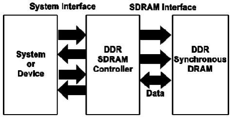
[image:2.595.306.557.122.201.2]To improve the speed of DRAM there is need for an additional design that work as a communicator between the device and the DRAM and also provide all the necessary signals for the functionality of the memory element. The mediator is called as controller or memory controller. It will perform all the basic command generation and provide the synchronization between memory and the device under operation.
[image:2.595.43.284.187.309.2]Figure 1. Basic block diagram for memory interface with device
Figure 1 shows the generalized block diagram for the memory element connected to the device via memory controller. In order to improve the latency and bandwidth synchronous protocol is use by the designer while developing DRAM based architecture. This makes the whole architecture as a synchronous DRAM (SDRAM). This type of architecture is very well known among the designers as it gives the user various added features such as improved speed, burst access and pipelined features. SDRAM controller can be built as per the application and used by the user as the only task of the controller is to initialize the memory and provide some
commands like refresh, Read, Write, etc. (Deepali et al., 2014)
As the microprocessors are getting faster these days the greatest challenge persists in improving the design of a controller to meet the technology. Development of Double data rate is one of the fantastic feature of SDRAM that improves the speed with double data rate and also provides the excellent throughput. For example if the design is working at 160MHz and transfers the data at the same rate based on the frequency in an ordinary SDRAM based design. Then by the use if DDRSDRAM the working frequency is improved to 320 MHz
and at the same time the data rate is doubled (Hegdeet al.,
2014).
Basics of DDR SDRAM
Necessary command set for DDRSDRAM is mentioned in table 1 that provides the quick overview of the command which are used for controlling of DDRSDRAM. All the signal work on the rising edge of the clock and are synchronous to the clock (Vu, 2014).
DDRSDRAM Controller
Controller main operation is to bridge the gap between the device in use and the memory element. It has got functionality
to generate signals such as initializing signals, power ON signal, read/write signal, address signals and data signals, etc. as per the requirement of the memory.
Table 1. DDRSDRAM Commands
Command Sign CS_N WE_N RAS_N CAS_N
No Operation NOP L H H H
Ld mode register MSR L L L L
Precharge PRE L L H L
Read READ L H L H
Write WRITE L H L L
Active ACT L L H H
Auto Refresh REF L L L H
Proposed architecture
The design of DDRSDRAM controller mainly comprises of
3 main modules: 1) Dataflow Module, 2) Control Module and
3) Finite State Machine used for generation of read and write related signals.
Data Flow Module: The functionality of the data flow module
is to act as a bus interface between the device in operation and SDRAM. The data flow module is shown as one of the block in fig 2. It has got some set of registers which are used to take the data from the user interface and transfer it to the memory at 2X clock domain. It is also responsible for taking the data from the controller and transfer to the use at 1X clock cycle. This block is responsible for generation of DQS signal from the controller for the SDRAM for the specific operation (Ostler
et al., 2011).
Figure 2. Block diagram for DDRSDRAM controller
Control Module: The main functionality of this module is to take the commands from CMD input and decode it to generate the necessary signals such as READA, REFRESH, PRECHARGE, LOAD, etc. It is also responsible for taking the data from SADDRS and distributing over a set of required registers available in the control module for the necessary operations. The control module is as shown in Figure 2.
Finite State Machine: Figure 3 shows the FSM developed for
[image:2.595.311.556.424.595.2]stat, Write state, Load mode, refresh and precharge, etc. The state machine enters in the NOP mode if no command is given to the design and initializes the design and wait for the next instruction. On getting command it switches to load mode via. Load reg1 or load reg2. Based on the data either coming from memory or data coming from the device. Depending on read and write operation it enters to the read sate and write state and generates the required signal to perform the specified task. Once the task is completed the acknowledgement signal is generated and device is either refreshed or precharged and returned back to the load register state and wait for the next
[image:3.595.312.557.116.374.2]operation to be given as an input (Saldana et al., 2012).
Figure 3. Finite State Machine of DDR SDRAM
Implementation Results: The snapshots obtained for the
[image:3.595.306.556.128.598.2]developed architecture is given. The design was coded in VERILOG HDL and was synthesized on XILINX ISE 14.1 to obtain the results. Figure 4 shows the design summary, we can understand that the design occupy very less numbers of slices and LUTs and hence it was possible implement on XILINX Spartan III FPGA. From Fig 4 we can understand that the total device utilization for the DDRSDRAM Controller is only 22% with very less utilization of LUTs just 4%. This is very small indeed. Figure 5 shows the top level RTL schematic generated for the developed code. From the figure 6 it is clear that all the necessary signals are generated to achieve a very user friendly interface between the device and SDRAM. Behavioral functionality in the next section shows the clear picture of the simulation results obtain for the design.
Figure 4. Design summary for developed System
Functional Simulation and Analysis of DDRSDRAM controller:
The designed architecture in the paper is verified using behavioral simulation of each and every module based on
[image:3.595.38.288.203.393.2]MODELSIM Simulator 6.3c. All the functional behavioral such as read and write operation has been tested and verified. Below in Figure 7 shows the simulation for the read operation mode of the designed Controller.
Figure 5. RTL Top Level Schematic
Figure 6. RTL Internal Architecture
[image:3.595.310.561.403.635.2] [image:3.595.39.298.606.694.2]Figure 7. Simulation Results for Read operation
[image:4.595.52.557.418.714.2]Conclusion
During the development of the DDRSDRAM controller we have analyzed that the design is bit tricky and complex due to enormous logic and timing constrained involved in it. It is very necessary that the design is developed with all attention. Based on our implementation we can conclude the designed architecture has all the necessary functionality and meets the requirement of DDRSDRAM controller and is also compatible to high speed bus such as PCI Express as per our requirements. The whole design was developed based on XILINX Spartan 3 FPGA family and was tested and implemented on the same for the hardware verification with seamlessly writing and reading operation performed. The design has been verified based on the functional verification and hardware implementation.
REFERENCES
Aguiar A. and F. Hessel, "Embedded systems' virtualization: The next challenge?"2015, Rapid System Prototyping, 21st IEEE International Symposium on, pp1-7
Deepali Sharma, Shrutibhargava, Mahendra Vucha, 2014. “Design and VLSI Implementation of DDR SDRAM Controller for High Speed Applications”, (IJCSIT) International Journal of Computer Science, PP-23-26. Hegde R., G. Mishra and K. S. Gurumurthy, 2014. "An insight
into the hardware and software complexity of ECUs in
vehicles" in Advances in Computing and Information
Technology, ser. Communications in Computer and
Information Science, vol. 198, PP-56-60.
Heithecker, S. and Ernst, R. 2015. “Traffic Shaping for An FPGA Based SDRAM Controller with Complex QoS Requirements”, Design Automation Conference 2005, June, pp. 575-578.
Kangmin Lee, Chi- Weon Yoon, Ramchan Woo, Jeong-Him Kook, Ja-I1 Koo'", Tae-Sung Jung*, and Hoi-Jim Yoo, 2016. “A Comparative Performance Analysis of a DDR-SDRAM, a D-RDRAM, and a DDR-FCRAM using a POPeye Simulator”, IEEE.
Ostler P. S., M. J. Wirthlin and J. E. Jensen, 2011. "FPGA
Bootstrapping on PCIe Using Partial
Reconfiguration", International Conference on
Reconfigurable Computing and FPGAs, pp. 380-385. Saldana M., A. Patel, H. J. Liu and P. Chow, 2012. "Using
Partial Reconfiguration and Message Passing to Enable FPGA-Based Generic Computing Platforms", International Journal of Reconfigurable Computing, PP 456-460. Vu, D. V. 2014. "Enabling partial reconfiguration for
coprocessors in mixed criticality multicore systems using PCI Express Single-Root I/O Virtualization", International Conference on Reconfigurable Computing and FPGAs,PP-345-360.