This paper is made available online in accordance with
publisher policies. Please scroll down to view the document
itself. Please refer to the repository record for this item and our
policy information available from the repository home page for
further information.
To see the final version of this paper please visit the publisher’s website.
Access to the published version may require a subscription.
Author(s): S.M. Thomas, T.E. Whall, E.H.C. Parker, D.R. Leadley,
R.J.P. Lander, G. Vellianitis and J.R. Watling
Article Title: Improved effective mobility extraction in MOSFETs
Year of publication: 2009
Link to published version:
*Corresponding Author Address: Department of Physics, University of Warwick, Coventry,
CV4 7AL, UK.
E-mail address
Tel. no.
024765 22448.
Fax
no.
02476 150897
Improved effective mobility extraction in SOI MOSFETs.
S.M. Thomasa*, T.E. Whalla, E.H.C. Parkera, D.R. Leadleya, R.J.P Landerb, G. Vellianitisb, J.R. Watlingc
a
Department of Physics, University of Warwick, Coventry, CV4 7AL, UK
bNXP Semiconductors, Kapeldreef 75, 3001 Leuven, Belgium
c
Device Modelling Group, Department of Electronics and Electrical Engineering, University of Glasgow,
Glasgow, G12 8LT, UK.
Abstract
The standard method of extracting a carrier
effective mobility from electrical measurements
on MOSFETs is reviewed and the assumptions
implicit in this method are discussed. A novel
technique is suggested that corrects for the
difference in drain bias during IV and CV
measurements. It is further shown that the lateral
field and diffusion corrections, which are both
commonly neglected, in fact cancel. The
effectiveness of the proposed technique is
demonstrated by application to data measured on
a quasi- planar SOI MOSFET at 300 K and 4 K.
Keywords: Mobility, SOI, finFET, MOSFET
1. Introduction
The operation of a silicon MOSFET requires
charge carriers to travel between its source and
drain contacts, so any scattering of these carriers
will limit the performance. The degree of carrier
scattering can be quantified through the carrier
mobility, which is proportional to the time
between scattering events and represents the
ability of a carrier to be accelerated in an electric
field. By comparing the experimental mobility
with model calculations over a range of carrier
densities (or gate voltage Vg) and temperatures it
is possible to work out which scattering
mechanism are dominant in each region.
However, the carrier mobility is not directly
measured, but must be correctly extracted from
the experimental data.
For bulk Si MOSFETs the effective mobility μeff
has been extracted from numerous devices and
found to follow a universal curve that depends
only on the vertical electric field (Eeff) across the
the carrier transit time there is a need for tighter
electrostatic control, which results in and
increase in Eeff and a decrease in the effective
mobility. Furthermore, access resistance has to
be kept low, to avoid RC time constants limiting
device switching speed, which entails heavy
doping in the source and drain regions and also
increases carrier scattering. This means that
conventional scaling results in a significant drop
in carrier mobility in small devices.
Beyond simple scaling, significant progress has
been made in achieving electrostatic control
through multiple gates and fabrication of
MOSFETs on SOI. Similarly, developments in
high-k gate dielectrics have led to reduced
effective oxide thicknesses and smaller gate
voltages, but at the cost of further scattering at
the channel-gate dielectric interface. In each
case it is important to know how the carrier
scattering has changed and which factors limit
the mobility. However, there are many pitfalls in
extracting μeff from a fabricated device that can
lead to erroneous conclusions.
In this paper we will discuss some commonly
neglected corrections that should be applied
when extracting the effective mobility of a
MOSFET. We will propose a simple approach
to correct the major source of error and show that
others in fact cancel out. Finally, the method
will be applied to data from wide finFETs at
room temperature and 4 K.
2. Review of conventional approach
We will begin by following the usual method of
extracting μeff for a MOSFET and identifying
four sources of error. The effective mobility is
commonly obtained by measuring the
conductivity, from the drain current Id at a drain
bias of Vd, and dividing by the inversion charge
density Qinv using
d eff
d inv
I
L
W V Q
µ =
(1)where W is the device width and L the channel
length.
The 1st source of error is the value of inversion
charge used.
The inversion charge density is often simply
calculated as Qinv =Cox(Vg−Vt) WL where Cox is
the measured oxide capacitance and Vt is the
(often ill defined) threshold voltage. Improved
accuracy can be obtained by using the split CV
(capacitance-voltage) method [1], and integrating
the measured gate-channel capacitance Cgc
( )
Vto find the charge in the channel
( )
1
Vg( )
inv g gc
Q
V
C
V dV
WL
−∞=
∫
(2).3
charge trapping in the dielectric, do not affect the
measurement of Cgc. Thus, the most commonly
used expression to extract μeff for a MOSFET is
2
g d eff V
d gc
L I
V
C dV
µ
−∞
=
∫
(3)Equation (3) can also be expressed by replacing
d d
I V with the drain conductance
d d d dI dV
g =
( )
2g d eff g V
gc
L g
V
C dV
µ
−∞
=
∫
, (4)but clearly this will lead to discrepancies where
the conductivity is non-linear.
The 2nd source of error is in combining data
obtained with a different drain bias.
During the measurement of Id a fixed drain bias
Vd is applied, while the gate voltage is swept
from below threshold to strong inversion.
However, the inversion charge is usually
measured from a CV scan with zero drain bias.
This can lead to significant errors as the presence
of a drain bias changes the charge distribution in
the channel.
Ideally the conductivity would be measured at
very low bias, but then noise is an issue so many
( )
d g
I V measurements use Vd = 50 mV [2,3,4]
and in some cases 100 mV [5] or larger which
creates a non-uniform channel. Alternative CV
techniques have been devised that measure the
gate-to-drain and gate-to-source capacitances
separately whilst biasing the substrate and the
source to create the same conditions as in the
( )
d g
I V measurement [6,7]. Modeling the
channel as a transmission line network has also
been employed with high frequency AC
admittance measurements [8]. In each case, the
measurement configurations are cumbersome
and cannot be used for SOI devices that do not
have a substrate contact.
In the next section, we will demonstrate a new
and simple technique to extract either I Vd d or
d d d dI dV
g = at Vd = 0 V , without resorting to
elaborate measurement procedure, and combine
this with an inversion charge from using the
normal split CV setup [1].
There are, however, two further sources of error
that should first be addressed by recapitulating
the full expression for the drain current in an
nMOSFET, which is composed of both drift and
diffusion contributions [9]
inv d inv eff x
dQ
I
W
Q
E
D
dx
µ
=
−
(5)where Ex is the electric field a distance x along
the channel and D is the diffusion coefficient.
The 3rd source of error is in neglecting the
diffusion term in the drain current.
neglected before pinch-off, after that point all
conduction at the drain end of the channel is by
diffusion. Similarly the drain current is
dominated by diffusion in the sub-threshold
region. The diffusion coefficient is given by the
well known Einstein relation D=εdµeff /q,
where q is the electronic charge and
ε
d is the diffusion energy [10]. For single subbandoccupancy, ,
( )
(
1 EF E0/kT)
ln 1{
(EF E0)/kT}
d kT e e
ε − − −
= + + with EF
being the Fermi energy, and E0 the first sub-band
minimum. This reduces to εd =kT in weak
inversion andεd =EF−E0 in strong inversion.
The 4th source of error is in assuming the drain
voltage is dropped linearly along the channel.
It is often assumed that the lateral field is
constant i.e., Ex = Vd/L, but this will not be the
case in short channel devices, especially near to
the source.
Providing Vd tends to zero, Sodini et al.[11]
suggest these last two errors can be corrected for
by making use of
(
)
x g d
E
=
F V V
L
, (6)and 2
(
)
WL
V
F
V
C
dx
dQ
inv=
−
ox d g. (7)
Using Eqs. (5-7) we may write
( )
d d d ox
eff g inv
I
V
C
F V
Q
W
L
q WL
ε
µ
=
+
(8)And including the correct expression Eq. (2) for
Qinv
(
)
( )
2
g d d
eff V
d
g gc ox
I V
L
F V
C dV
C
q
µ
ε
−∞
=
+
∫
(9)
Although Eq. (9) is simple enough, it was not
explicitly stated in the original paper by Sodini et
al.[11]. They did state that the two corrections
have a “canceling effect”, but again did not show
this explicitly. Unfortunately, Sodini et al.’s
expression for F(Cgc/Cox), which was originally
derived for bulk MOSFETs, gives unphysically
large values of the mobility in the present case.
More recently Zebrev and Gorbunov [12] have
given a drift diffusion model for a fully depleted
SOI MOSFET, from which
1
1
ox dinv
C
F
qQ WL
ε
β
−
=
+
, (10)where
(
S BOX)
oxBOX S
C
C
C
C
C
+
+
=
1
β
and CS, CBOXand Cox are the capacitance of the silicon body,
buried oxide and gate oxide respectively.
In the case where Cox >> CBOX, CS, and hence
β = 1, it can easily be seen by substituting
Eq. (10) into Eq. (8), that any variation in the
5
diffusion term, leaving the original “uncorrected”
Eq. (3). However, the particular capacitance
values must first be assessed to check β = 1
before making this assumption.
3. Proposed, improved approach
Following the above discussion we propose a
new and simple technique to extract the effective
mobility. The inversion charge is measured as a
function of gate voltage using the normal split
CV setup [1]. We then measure sets of
( )
d g
I V
for different drain biases and perform linear
regression to obtain the limiting value of either
Id/Vd or gd =dId dVd at Vd = 0 V. The approach
is somewhat different in the regions of
sub-threshold and strong inversion:
The drain current in sub-threshold is due to
diffusion and given by
0
1
d qV
kT d
I
=
I
−
e
−
(11)So 0
d qV
d kT
d d
dI
q
g
I
e
dV
kT
−
=
=
, (12)or
ln(
g
d)
q
V
dln
q
I
0kT
kT
= −
+
(13)Hence a plot of ln(gd) against Vd, at a particular
gate voltage, is a straight line with the intercept
yielding gd
(
V Vg, d =0) ( )
=I V0 g q kT. Note thatin the limit of small Vd Eq. (11) reduces to
0
d d
I =I qV kT, so
d d
I V is numerically equal to
d
g in the limit of Vd =0. The predicted slope of
–q/kT can be used to check the extraction is
valid. Beyond threshold the drift term becomes
dominant and the slope of the semi-log plot will
be seen to deviate from –q/kT. In the strong
inversion region, plots of Id/Vd against Vd for
given gate voltage yield straight lines with the
obvious intercepts of Id/Vd at Vd = 0V.
4. Measurements on finFET devices
To test the suggested methodology the various
corrections are applied to a finFET of width
1.87 μm, at 300 K and 4 K. In research, wide
finFETs (quasi-planar) serve as controls in
comparing their narrow fin counterparts with
standard top-gated MOSFETs. N-channel
finFETs were fabricated at NXP Semiconductors
on Si(100) substrates, with 145 nm buried SiO2
and 65 nm SOI with a doping of 1015cm-3. Fins
were defined in the <110> direction with (110)
sidewall surfaces and a (100) top surface. The
gate stacks consisted of 1 nm thermal SiO2
followed by metal organic chemical vapour
deposition of 2.3 nm Hf0.4Si0.6O and 5 nm TiN
deposited by plasma enhanced atomic layer
deposition. After gate patterning, As extensions
were implanted and spacers formed. Access
epitaxy. As+P highly doped drain implantation
and NiSi were used for source/drain contacts
with a spike anneal at 1050oC to activate the
dopants. A cross sectional TEM image of a
device with a fin width of 13 nm is shown in
Fig. 1. Additional details can be found in
[image:7.595.133.236.247.442.2][13][14].
Figure 1: Cross sectional TEM image of a 13nm
finFET after full device processing.[14]
In this work a quasi-planar device was
investigated consisting of 10 parallel fins, each
of width (Wfin) 1.872 μm, height (Hfin) 65 nm and
length (L) 10 μm. The effective width is given
by Weff = 10*(2Hfin+Wfin) = 20µm. We measured
Id(Vg) for drain biases in the range Vd = 5–
100 mV and Cgc(Vg) at a frequency of 100kHz
both at 4K and 300K. We found that the access
resistance was indeed negligible compared to the
channel resistance for these long channel
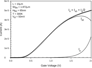
devices. However, at large gate voltage the
measured drain current is reduced (Id0 in Fig. 2)
due to gate leakage. This has been corrected for
by adding back the gate leakage current Ig using
2
0 g
d d I I
I = + (as half the leakage current is to
the source, half to the drain and body leakage can
be ignored in the SOI structure) [15]. Figure 2
shows how this removes the apparent drop in
drive current at high gate voltage.
Gate Voltage (V)
0.0 0.5 1.0 1.5 2.0
C
u
rre
n
t
(A
)
0 1e-5 2e-5 3e-5 4e-5 5e-5 6e-5
Id = Id0 + Ig/2
Id0
Ig
[image:7.595.314.503.293.432.2]L = 10µm Wfin = 1.872µm Hfin = 65nm T = 300K Vd = 50mV
Figure 2: Gate leakage correction: Id0 and Ig are
the measured drain and gate leakage currents, Id
is the corrected drain current.
Gate Voltage (V)
0.0 0.5 1.0 1.5 2.0
Id
(A
)
1e-14 1e-13 1e-12 1e-11 1e-10 1e-9 1e-8 1e-7 1e-6 1e-5 1e-4 1e-3
Vd = 10mV
Vd = 35mV
Vd = 60mV Vd = 100mV
L = 10µm Wfin = 1.872µm Hfin = 65nm T = 300K
Vd = 50mV
Figure 3: Corrected Id(Vg) data for a range of drain biases at 300 K.
Figure 3 shows the leakage corrected
( )
d g
I V at
room temperature for a range of drain bias
[image:7.595.313.505.496.631.2]7
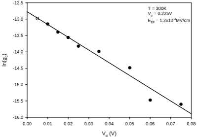
be extracted for any chosen Vg. Figures 4 and 5
show examples of the regression used in
sub-threshold, at Vg = 0.225 V, and in strong
inversion at Vg = 0.70 V, respectively.
Vd (V)
0.00 0.01 0.02 0.03 0.04 0.05 0.06 0.07 0.08
ln
(gd
)
-16.0 -15.5 -15.0 -14.5 -14.0 -13.5 -13.0 -12.5
T = 300K Vg = 0.225V
EEff = 1.2x10 -3
[image:8.595.85.285.185.324.2]MV/cm
Figure 4: Semi-log variation of drain conductance gd with drain bias in the sub-threshold region (Vg = 0.225 V), enabling
gd(Vd = 0) to be extracted as the intercept.
Vd (V)
0.00 0.01 0.02 0.03 0.04 0.05 0.06 0.07 0.08
Id
/V
d
(S
)
2.3e-4 2.4e-4 2.5e-4 2.6e-4 2.7e-4 2.8e-4
T = 300K Vg = 0.7V
[image:8.595.87.282.393.532.2]EEff = 0.13MV/cm
Figure 5: Variation of drain current with bias in
strong inversion (Vg = 0.70 V) from which the zero bias conductance can be extrapolated.
In each case we see the predicted straight line
behavior and are able to extract a conductance
value for zero bias. Fig. 4 has the correct slope
of -38 V-1 and typical regression coefficients are
better than 0.98, indicating high accuracy. Note
that the conductance in strong inversion (where
channel mobility is often reported) is already 8 %
lower at the standard measuring bias of
Vd = 50 mV than at zero bias.
We have also performed these measurements at
low temperatures (4 K), where fewer scattering
mechanisms need to be considered making the
mobility results simpler to interpret, and again
obtain good linear fits from which to extract zero
bias conductivity values.
5. Carrier mobility in finFET devices
Having extracted the zero bias conductance
values corresponding to each inversion charge
density the electron mobility can be calculated
with the first two errors corrected, as shown in
Fig. 6 for the 4 K data as a function of Qinv. The
large suppression of inferred mobility at higher
drain bias can clearly been seen, especially at
low density, confirming the necessity of
extrapolating to Vd = 0 V.
Ninv (cm-2)
1.0e+12 3.0e+12 5.0e+12 7.0e+12 9.0e+12 1.1e+13
E
ff
e
ct
iv
e
M
o
b
ilit
y
(
cm
2V -1s -1)
0 200 400 600 800 1000 1200
Increasing Vd
L = 10µm Wfin = 1.872µm
Hfin = 65nm
Vd:10mV to 100mV
T = 4K
Figure 6: Extracted mobility at 4 K, showing the
[image:8.595.313.508.509.652.2]Ninv (cm -2
)
1.0e+12 3.0e+12 5.0e+12 7.0e+12 9.0e+12 1.1e+13
E
ff
e
c
ti
v
e
M
o
b
ilit
y
(
c
m
2V -1s -1)
0 200 400 600 800 1000 1200
Drift only Vd = 50mV
L = 10µm Wfin = 1.872µm
Hfin = 65nm
T = 4K
Vd correction
Vd + Diffusion correction
[image:9.595.86.282.88.229.2]Vd + Diffusion + E-field correction
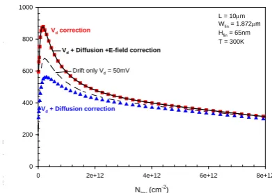
Figure 7: 4 K mobility values: uncorrected
(broken line) and including corrections for drain bias only (squares), drain bias and diffusion (triangles), drain bias, diffusion and Ex-field (solid line).
Next we consider the additional corrections that
arise from including carrier diffusion and
non-uniform electric field along the channel. In order
to consider the diffusion correction over the full
range of gate biases we have calculated the
Fermi energy in the quasi-2D electron gas, (the
inversion layer) using a Poisson-Schrödinger
simulator [16,17]. Figure. 7 shows how this
diffusion correction reduces the mobility values
extracted, particularly at high density, and how
the further correction for non-uniform field
exactly cancels this effect at all gate voltages.
A similar procedure has been followed for
the room temperature data, shown in Fig. 8.
Ninv (cm -2
)
0 2e+12 4e+12 6e+12 8e+12
Ef
f
ti
M
b
ilit
(
V
)
0 200 400 600 800 1000
L = 10µm Wfin = 1.872µm
Hfin = 65nm
T = 300K
Vd correction
Vd + Diffusion correction Drift only Vd = 50mV
[image:9.595.310.506.97.236.2]Vd + Diffusion +E-field correction
Figure 8: Mobility extracted from room
temperature data, showing the effect of the various corrections as in Figure 7.
An interesting feature of the 300 K mobility is
the sharp peak near threshold. Iyengar et al.[18]
have seen this on the top surface of their finFETs
with HfSiO gate dielectric, but offer no physical
explanation. This pronounced peak is only
observed in our wide quasi-planar finFETs
(Wfin > 65 nm) and not for the devices with
narrow fins. The magnitude of the peak is also
very sensitive to variations in Qinv. In the present
case, the steep drop to the left of the peak in
Fig. 8 is at least partially due to trapping
processes that affect the CV measurement [19]
and may be obviated by inversion charge
pumping [20]. The fully corrected mobility
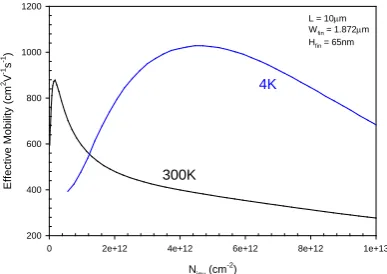
values at 300 K and 4 K (solid lines from Figs. 7
and 8) are compared in Fig. 9. This shows that
the anomalous peak at low density in the room
temperature mobility leads to a higher mobility
in that region for 300 K than at 4 K, contrary to
9
an explanation for this either, but suspect that it
may be related to the inversion charge density
measurement close to threshold and suggest
further work on this is required.
E-Field MV/cm vs Mob + Vd + Diff + E E-Field (MV/cm) vs Mob + Vd + Diff + E
Ninv (cm -2
)
0 2e+12 4e+12 6e+12 8e+12 1e+13
E
ff
e
c
tiv
e
M
o
b
ilit
y
(
c
m
2V -1s -1)
200 400 600 800 1000 1200
4K
300K
L = 10µm Wfin = 1.872µm
[image:10.595.86.280.195.332.2]Hfin = 65nm
Figure 9: Comparison of the fully corrected
mobility at 300 K and 4 K in a wide finFET.
6. Conclusion
Accurate mobility extraction is essential for
assessing the benefits to be gained from novel
device architectures and use of “high-mobility”
channel materials, such as strained silicon or
germanium. It is also vital to understand the
relationship between experimentally extracted
quantities and those used in device modeling.
The usual method of mobility extraction has
tended to ignore the difference in drain bias
during IV and CV measurements. Whilst
previous attempts to accommodate this have
resulted in elaborate measurement techniques,
we suggest a novel method to correct for the
drain bias in the IV measurements so that the
effective mobility is essentially extracted at zero
drain bias. Furthermore, corrections for a
non-uniform electric field in the channel and for the
diffusion contribution to the drain current have
been considered. Although these individually
have a significant effect, when applied in
combination they are shown to exactly cancel for
the whole gate voltage range. Consequently
provided that one is ignored they both can be!
The methodology has been applied to extract
effective mobility from experimental data on an
SOI quasi-planar finFET, both at room
temperature and 4 K. This has demonstrated that
a drain bias of only 50 mV has a significant
effect on the values obtained. Finally, we
suggest that the drain bias correction can, and
should, also be applied to ordinary bulk
MOSFETs.
Acknowledgements
This research has received funding from
EPSRC(UK) and the EC Seventh Framework
Programme (FP7/2007-2013) under Nanosil,
grant n°216171. Simulation services for results
presented here were provided by the Network for
Computational Nanotechnology (NCN) at
6. References
[1] Koomen, J., Solid State Electron., 16, 801,
(1973)
[2] Wang, J, Kistler, N., Woo, J., Viswanathan,
C.R. IEEE Electron Device Letters, 15, 117,
(1994)
[3] Takagi, S., Toriumi, A., Iwase, M., Tango, H.
IEEE Trans. Electron Devices, 41, 2357, (1994)
[4]Kilchytska, V., Lederer, D., Collaert, N. et al.
IEEE Electron Device Letters, 26, 749, (2005)
[5]Ramos, J., Augendre, E., Kottantharayil, A.
et al. Proc. Solid-State Integr.Circuit Technol.8,
72, (2006)
[6] Huang, C. L., Faricelli, J. V. and Arora, N. D.
IEEE Trans Electron Dev, 40, 1134, (1993)
[7] Koga, J., Takagi, S., Toriumi, A., Int. Conf.
Solid State Devices and Materials, 895, (1994)
[8] Chow, P. D. and Wang, K. IEEE Trans
Electron Dev, 33, 1299, (1986)
[9] Schroder, D.K., “Semiconductor Material
and Device Characterization (2nd Ed.)” Wiley,
(1998)
[10] Baccarani,G., Gnani,E., Gnudi,A.,
Reggiani,S., Rudan,M. Solid State Electronics,
52, 526, (2008)
[11] Sodini, C. G., Ekstedt, T. W. and Moll, J. L.
Solid State Electronics, 25, 833, (1982)
[12] Zebrev, G.I., Gorbunov, M.S. Proc. MIEL
(2006)
[13] Dal, M.J.H., et al. VLSI Tech. Dig. 110,
(2007)
[14] Vellianitis, G., et al.IEDM, 681, (2007)
[15] Zeitzoff, P. M., Young, C. D., Brown, G. A.
and Kim, Y. IEEEElectron Device Letters, 24,
275, (2003)
[16] Vasileska, D., Ahmed, S. S., Mannino, M.,
Matsudaira, A., Klimeck, G., Lundstrom, M.
“Schred
[17] Vasileska, D., Schroder, D. K. and Ferry,
D.K. IEEE Trans. Electron Devices44, 584,
(1997)
[18] Iyengar, V.V., et al. IEEE Trans Electron
Dev, 54, 1177, (2007)
[19] Kapila, G., Kaczer, B., Nackaerts, A.,
Collaert, N., Groeseneken, G. V.IEEE Electron
Device Letters, 28, 232, (2007)
[20] Kerber, A., Cartier, E., Ragnarsson, L. A.,
Rosmeulen, M., Pantisano, L., Degraeve, R.,
Kim, Y., Groeseneken, G. Symp. VLSI Tech.