A Thesis Submitted for the Degree of PhD at the University of Warwick
http://go.warwick.ac.uk/wrap/2795
This thesis is made available online and is protected by original copyright. Please scroll down to view the document itself.
User’s Declaration
AUTHOR: Vishal Ajit Shah DEGREE: Ph.D.
TITLE: Reverse Graded High Content (x>0.75) Si1-xGex
DATE OF DEPOSIT:……….
Virtual Substrates
I agree that this thesis shall be available in accordance with the regulations governing the University of Warwick theses.
I agree that the summary of this thesis may be submitted for publication.
I agree that the thesis may be photocopied (single copies for study purposes only).
Theses with no restriction on photocopying will also be made available to the British Library for microfilming. The British Library may supply copies to individuals or libraries. Subject to a statement from them that the copy is supplied for non-publishing purposes. All copies supplied by the British Library will carry the following statement:
“Attention is drawn to the fact that the copyright of this thesis rests with its author. This copy of the thesis has been supplied on the condition that anyone who consults it is understood to recognise that its copyright rests with its author and that no quotation from the thesis and no information derived from it may be published without the author’s written consent.”
AUTHOR’S SIGNATURE:……….
_________________________________________________________________________
1. I undertake not to quote or make use of any information from this thesis without making acknowledgement to the author.
USER’S DECLARATION
2. I further undertake to allow no-one else to use this thesis while it is in my care.
DATE SIGNATURE ADDRESS
………
……… ………
Title Page
Reverse Graded High Content
(x>0.75) Si
1-x
Ge
x
Virtual Substrates
by
Vishal Ajit Shah
Thesis
Submitted to the University of Warwick
in partial fulfilment of the requirements
for admission to the degree of
Doctor of Philosophy
Declaration
This thesis is submitted to the University of Warwick in support of my application
for the degree of Doctor of Philosophy. All experimental data presented was carried
Abstract
Silicon germanium alloy layers can be grown epitaxially on a silicon substrate to
provide a means of adjusting the lattice parameter of the crystal. Such a platform,
known as a virtual substrate, has a number of potential applications. For instance, it
allows for subsequent overgrowth of highly strained layers of silicon, or germanium,
that could enable very high speed transistors, similarly it could be used as the starting
point of a range a silicon-based optoelectronic devices. In this work, a novel
adaptation has been made to a recently proposed reverse grading technique to create
high Ge composition SiGe virtual substrates. The proposed structures consist of a
relaxed, highly defected, pure Ge underlayer on a Si (001) substrate prior to reverse
grading where structures have final compositions of Si0.2Ge0.8. Additionally, two
grading schemes are studied, reverse linear grading and reverse terrace grading. All
buffers are grown by reduced pressure chemical vapour deposition. The relaxation,
defect levels and surface roughness of the fabricated buffers have been quantified
whilst varying the grading rate.
An ideal grading rate has been found where the quality of the buffer is very high, due
to the highly defected Ge underlayer and that the buffer relaxes under tensile strain.
Outside of this ideal grading rate three dimensional growth, stacking fault formation
and crack generation can occur. Cracking of the buffer has been modelled and some
conditions where the buffer is stable have been found. This study experimentally
Publications and Presentations
(Resulting directly from the study presented:)
Refereed Publications
1)V. A. Shah, A. Dobbie, M. Myronov, D. J. F. Fulgoni, L. J. Nash, and D. R. Leadley, Reverse graded relaxed buffers for high Ge content SiGe virtual substrates, Applied Physics Letters 93, 3 (2008).
2)V. A. Shah, A. Dobbie, M. Myronov, D. J. F. Fulgoni, L. J. Nash, and D. R. Leadley, Reverse graded SiGe/Ge/Si buffers for high-composition virtual substrates, Journal of Applied Physics (submitted 2009)
Conference Presentations
1) Reverse graded relaxed buffers for high Ge content SiGe virtual substrates (oral)
European Materials Research Society (E-MRS) 2008, May 26-30, 2008, Strasbourg, France
2) Epitaxial growth of compressive strained Ge layers on reverse linearly graded virtual substrate by RP-CVD (oral)
V. A. Shah, D. R. Leadley, E. H. C. Parker, J. Parsons, D. Fulgoni
European Materials Research Society (E-MRS) 2009, June 8-12, 2009, Strasbourg, France
M. Myronov, A. Dobbie, V.A. Shah, X.C. Liu, Van H. Nguyen and D.R. Leadley
3) Low temperature epitaxial growth of compressive strained Ge layers on reverse linearly graded virtual substrate by RP-CVD (oral)
6th
M. Myronov, A. Dobbie, V.A. Shah, X.C. Liu, Van H. Nguyen and D.R. Leadley International Conference on Silicon Epitaxy and Heterostructures (ICSI-6), May 17 - 22, 2009, Los Angeles, California, USA
4) Compressively strained Ge channel heterostructures grown by RP-CVD for the next generation CMOS devices (to be accepted)
M. Myronov, V.A. Shah, A. Dobbie, Xue-Chao Liu, Van H. Nguyen and D.R. Leadley
5) Reverse graded virtual substrates for strained Ge devices (oral)
UK Semiconductors 2009, Sheffield, UK, July 1-2, 2009
D.R. Leadley, V.A. Shah, A. Dobbie, and M. Myronov
(Resulting from other work carried out during the duration of the thesis:)
Refereed Publications
1) P. M. Gammon, A. Perez-Tomas, M. R. Jennings, G. J. Roberts, M. C. Davis, V. A. Shah, S. E. Burrows, N. R. Wilson, J. A. Covington, and P. A.
Mawby, Characterization of n-n Ge/SiC heterojunction diodes
2) A. Perez-Tomas, M. R. Jennings, M. Davis, V. Shah, T. Grasby, J. A. Covington, and P. A. Mawby, High doped MBE Si p–n and n–n heterojunction diodes on 4H-SiC, Microelectronics Journal 38, 1233-1237 (2007).
, Applied Physics Letters 93 (2008).
3) A. Perez-Tomas, M. R. Jennings, M. Davis, J. A. Covington, P. A. Mawby, V. Shah, and T. Grasby, Characterization and modelling of n-n Si/SiC heterojunction diodes, Journal of Applied Physics 102, 5 (2007).
Conference Proceedings
1) Characterisation of p-n and n-n heterojunction diodes with high doped MBE Si on 4H-SiC
Proceedings of Workshop on Compound Semiconductor Devices and
Integrated Circuits in Europe (WOCSDICE) 2007, May 20-23, 2007, Venice, Italy
A. Pérez-Tomás, M. R. Jennings, M. Davis, V. Shah, T. Grasby, J. A. Covington and P. A. Mawby
A. Pérez-Tomás, M. R. Jennings, M. Davis, V. Shah, T. Grasby, J. A. Covington and P. A. Mawby
Meeting Presentations
1) Inducing Uniaxial Strain though Virtual Substrates
Institut fur Halbleitertechnik, Universitaet Stuttgart. 18th
V.A. Shah, T. Grasby, E. H. C. Parker.
Table of Contents
User’s Declaration
... i
Title Page
... ii
Declaration
... iii
Abstract
... iv
Publications and Presentations
... v
Table of Contents
... viii
List of Figures
... xii
List of Tables
... xxiv
Acknowledgements
... xxvi
1
Introduction
... 1
1.1 The Semiconductor Industry ... 1
1.2 Introduction to Strain Engineering... 2
1.3 Inducing Strain ... 5
1.4 Incorporation of Optoelectronic Materials ... 7
1.5 Scope of Work ... 8
1.5.1 Chapter Summaries ... 9
2
Theoretical Discussion
... 11
2.1 Basic Properties of Silicon Germanium ... 11
2.1.1 Other Parameters of Si, Ge and SiGe alloys ... 12
2.2 Epitaxial Growth Techniques ... 13
2.2.1 Reduced Pressure Chemical Vapour Deposition (RP-CVD) ... 14
2.2.2 Substrate Surface Preparation ... 15
2.2.3 Precursors ... 16
2.2.4 Chamber Etching ... 19
2.3 Growth Kinetics of Silicon-Germanium ... 20
2.3.1 Adatom Transport... 20
2.3.2 Growth Modes ... 22
2.4.4 Dislocation Motion ... 33
2.4.5 Nucleation of Dislocations ... 35
2.4.6 Critical Thickness and Dislocation Energetics ... 36
2.4.7 Interactions Between Dislocations ... 42
2.4.8 The Modified Frank-Read (MFR) Multiplication Mechanism ... 45
2.5 Relaxation of Reverse Graded Virtual Substrates ... 47
2.5.1 Tensile Strain Enhanced Smoothing... 48
2.5.2 Partial Dislocations and Stacking Faults ... 49
2.5.3 Graded Layer Critical Thicknesses... 54
2.5.4 Thermal Expansion... 56
2.5.5 Cracking ... 57
2.6 Relaxed Strain Buffers (RSB)... 62
2.6.1 Thick Constant Composition Layers ... 63
2.6.2 Step Graded Buffers ... 64
2.6.3 Linear Graded Buffers ... 65
2.6.4 Terrace Grading ... 69
2.6.5 Ge Condensation ... 70
2.6.6 Ion implantation ... 72
2.6.7 Low Temperature Method ... 74
2.6.8 Two Temperature Growth Method ... 75
2.6.9 Summary of Existing High Ge Content Buffers ... 77
2.6.10 Previous work on Reverse Grading ... 78
3
Experimental Techniques
... 80
3.1 Transmission Electron Microscopy (TEM) ... 80
3.1.1 Sample Preparation... 81
3.1.2 Image Formation ... 82
3.1.3 Image Contrast and Diffraction ... 84
3.2 Atomic Force Microscopy (AFM) ... 87
3.3 Differential Interference Contrast Microscopy (DIC)... 89
3.4 High Resolution X-Ray Diffractometry (HR-XRD) ... 91
3.4.1 Reciprocal Space Maps ... 93
3.4.2 Interpretation of Reciprocal Space Maps ... 95
3.4.3 X-Ray Reflectivity (XRR) ... 97
3.5 Selective Defect Etching ... 99
3.5.1 Dilute Schimmel Etchant ... 101
3.5.2 Dilute Iodine Etchant ... 101
3.5.3 Comparison of Etchants on High Composition SiGe Layers ... 102
3.6 Secondary Ion Mass Spectroscopy (SIMS) ... 106
4.1 Introduction ... 108
4.2 Reverse Graded Structures... 109
4.2.1 Design of Base Layer for Reverse Graded Structure ... 110
4.2.2 Base Layer Characteristics ... 111
4.2.3 Design of Reverse Linear Grade ... 112
4.2.4 Design of Reverse Terrace Grade ... 114
4.2.5 Growth Parameters ... 115
4.3 Properties of Reverse Linear Graded (RLG) Buffers ... 117
4.3.1 RLG Buffer Composition Profile ... 118
4.3.2 Surface Roughness of RLG Buffers ... 125
4.3.3 Dislocation Densities within RLG Buffers ... 129
4.3.4 Extended Stacking Faults within RLG Buffers ... 134
4.3.5 Cracking of RLG Buffers ... 137
4.3.6 Relaxation and Composition of RLG Buffers ... 143
4.4 Properties of Reverse Terrace Graded (RTG) Buffers ... 149
4.4.1 RTG Composition Profile ... 149
4.4.2 Surface Roughness of RTG Buffers ... 154
4.4.3 Dislocation Densities within RTG Buffers ... 157
4.4.4 Extended Stacking Faults in RTG buffers ... 161
4.4.5 Cracking of RTG Buffers ... 162
4.4.6 Relaxation and Composition of RTG Buffers ... 164
4.5 Truncated RTG Structures ... 166
4.5.1 Surface Roughness of Truncated RTG Buffers ... 167
4.5.2 Relaxation of Truncated RTG Buffers ... 170
4.5.3 Dislocation Densities within Truncated RTG Buffers ... 172
4.6 Modelling of Critical Thickness for Cracks ... 173
4.6.1 Dependence of Buffer Relaxation ... 173
4.6.2 Dependence of Buffer Thickness ... 177
4.7 Discussion and Conclusion ... 179
4.8 Comparisons with other buffer fabrication techniques ... 187
4.9 Summary ... 189
5
Development of Substrate Design
... 192
5.1 Introduction ... 192
5.1.1 Standard Relaxed Graded Layer ... 192
5.2 Optimising the Two Temperature Ge Underlayer ... 193
5.3.1 Layer Thickness ... 208
5.3.2 Relaxation and Composition ... 209
5.3.3 Defect Densities ... 211
5.3.4 Roughness ... 214
5.4 Optimising the Complete Reverse Graded Buffer ... 216
5.4.1 Thickness Optimised Designs ... 216
5.4.2 Characterisation of Thicker Optimised Buffer ... 219
5.4.3 Characterisation of Thinner Optimised Buffer ... 222
5.5 Discussion ... 224
5.6 Summary ... 226
6
Conclusion and Further Work
... 228
6.1 Conclusions ... 228
6.2 Further Work ... 233
List of Figures
Figure 1.1: A graph showing Moore’s law in action by plotting all the
commercial transistors’ release date versus the number of
transistors per chip [7]. ... 2
Figure 1.2: The heavy hole (HH) and light hole (LH) valence bands in a) bulk
germanium and b) compressively strained germanium... 4
Figure 1.3: The bandgap dependence of Si1-xGex alloys on the Ge content (x)
of the alloy. Taken from Paul [2]. ... 6
Figure 1.4: A graph of various semiconductors’ bandgaps and their lattice
parameters. Adapted from Veeco[18]. ... 8
Figure 2.1: A schematic of a face centred diamond cubic crystal. The quantity
a is defined as the lattice parameter. ... 12
Figure 2.2: A simple schematic representation of a generic CVD chamber. ... 15
Figure 2.3: A diagram showing the different stages of precursor deposition of
germane on a Si (001) substrate during epitaxy. ... 17
Figure 2.4: Growth rates as a function of temperature when compared to work
performed on SiH4 (silane, Everstey [28]), SiH2Cl2 (Everstey
[28]) and GeH4 (Cunningham [29]). Work done by Cunningham
et al was performed within an ultra high vacuum CVD. ... 19
Figure 2.5: Diagram of typical adatom sites and defects which outline adatom
transport. Taken from Hudson [33]. ... 21
Figure 2.6: Schematic representation of the tree different epitaxial growth
modes with are achievable; a) Frank van-der Merwe, b)
Volmer-Weber and c) Stranski-Krastanov. ... 23
Figure 2.7: Diagram showing the tetragonal distortion of a cubic lattice and
the resultant effect on the lateral and vertical lattice parameters
under a) compressive and b) tensile strain. Adapted from Parsons
[38]. ... 25
to create a complete circuit around the dislocation when equal amounts of bonds in opposite directions are taken into account. ... 29
Figure 2.9: A schematic of the 60° dislocation Burgers vector direction. Also
shown is beff, the effective Burgers vector which participates in
strain relaxation. Adapted from Nash [40] ... 30
Figure 2.10: A physical representation of the threading and misfit dislocations
as the boundary of a slipped plane which shows the order of
bonds which are broken. Adapted from Parsons [38]. ... 31
Figure 2.11: A diagram of the plane of the closest packed atoms showing the
threading dislocation glide through the strained layer and the
associated extension of the misfit dislocation. ... 34
Figure 2.12: The Matthews-Blakeslee model for the generation of misfit
dislocations. Shown are the forces acting on a threading
dislocation arm. Adapted from People and Bean [14] ... 37
Figure 2.13: The model proposed by People and Bean to nucleate dislocation
half loops in a dislocation free mismatched material system.
Taken from People and Bean [14]... 39
Figure 2.14: The calculated critical thicknesses from the People-Bean and
Matthews-Blakeslee criterion for SiGe layers grown on a relaxed
Ge layer. ... 42
Figure 2.15: The interaction of a threading dislocation with the strain field of
another orthogonal misfit dislocation. Splitting of the threading
arm can occur and the effective channel for glide is then reduced.
Taken from Parsons [38]. ... 43
Figure 2.16: A schematic representation of the modified Frank-Read (MFR)
dislocation multiplication mechanism process. Two misfit
dislocations which have formed a corner are pushed into the
substrate and each misfit dislocation moves on different glide
planes. A they are pushed further into the substrate they then form
a dislocation loop which then in turn creates a misfit dislocation
with threading arms. i) shows the characteristic <110> profile of
the MFR mechanism. Adapted from Capewell [53] ... 46
Figure 2.17: A schematic of the surface steps SA and SB on an unstrained
which are perpendicular to the steps on the SA terrace are shown
as horizontal black lines. Dimer bonds parallel to the SB terrace
are shown as black dots. Taken from Xie [54]. ... 48
Figure 2.18: A schematic of the directions of the different dislocation Burgers
vectors; a) 90°, b)60° and c) 30°. Also shown is beff, the effective
Burgers vector which participates in strain relaxation. Adapted
from Nash [40] ... 50
Figure 2.19: A schematic cross sectional view of a stacking fault which is
seen as the shaded region. This is caused by one 90° partial
dislocation at point P where the dislocation line direction is
[1-10]. The 30° is not shown in the diagram and would be positioned
off the page. Taken from Parsons [38]. ... 51
Figure 2.20: The formation of extended stacking faults and their features
which are formed by a) glide and b) nucleation. Adapted from
Marée [57] ... 52
Figure 2.21: Shows the critical thickness for the formation of a stacking fault
through glide and the Matthews-Blakeslee critical thickness for a
Si1-xGex layer on a relaxed Ge (001) surface. ... 54
Figure 2.22: The critical thicknesses of a (reverse) graded substrate which
starts on a pure Ge layer with a final composition of 0.8... 56
Figure 2.23: The cracking critical thicknesses for various pseudomorphic
SiGe layer compositions on a Ge (001) surface. ... 59
Figure 2.24: A cross section view of a “V” shaped crack, the dimensions used
in calculating the relaxation are labelled. Taken from Murray[64]. ... 60
Figure 2.25: A forward step graded Si1-xGex structure, graded up to Si0.2Ge0.8
in x = 0.2 compositional jumps. ... 64
Figure 2.26: An example of a forward linear graded Si1-xGex structure,
graded up to Si0.2Ge0.8 with a thick constant composition cap. ... 65
Figure 2.27: An example of a forward terrace graded Si1-xGex structure,
graded up to Si0.2Ge0.8 in x = 0.2 terraces with a thick constant
form b) an oxide layer on top of a higher Ge composition SiGe layer due to selective oxidisation. Taken from Nakaharai [86]. ... 71
Figure 2.29: The ion implantation process as reported by Hoshi [93]. ... 73
Figure 2.30: The low temperature (LT) buffer as reported by Peng [94]. The
LT layers are grown at 400°C and the high temperature (HT)
layers are grown at 550°C. ... 74
Figure 2.31: A schematic of the two temperature layer, as reported by
Hartmann [60]. ... 75
Figure 2.32: The reverse graded Si1-xGex structure reported by Wong [100]. ... 79
Figure 3.1: A schematic representation of a typical transmission electron
microscope. ... 82
Figure 3.2: A physical representation of the g•b invisibility criterion. a) Shows that when g•b=0, the distortion caused by the perfect edge dislocation is not observable when the Burgers vector is
perpendicular to the vector of view. b) Shows that when g•b≠0
the dislocation is visible. ... 85
Figure 3.3: a) The AFM head where the laser system is mounted. b) a TEM
micrograph of an AFM contact mode cantilever. The SiN tip can
be seen on the end of this cantilever. Both images were taken
from the Veeco Training manual [103]. ... 87
Figure 3.4: A schematic of the AFM system. The piezoelectric motor is
moved laterally to perform a scan and when the cantilever is
deflected the control system lowers the stage until no deflection
of the reflected laser is measured. ... 88
Figure 3.5: A schematic of a typical DIC microscope. Adapted from Nash
[40]. ... 90
Figure 3.6: A schematic of the XRD system used in this study. ... 92
Figure 3.7: A schematic of the degrees of freedom that the diffracting stage
was able to achieve. ... 92
Figure 3.8: A schematic of the reciprocal space points which correspond to all
the accessible different planes in a (001) orientated crystal lattice.
The physical axes are shown along with the [004] and the [224]
Figure 3.9: Crystal planes analysed by XRD. a) shows how the epitaxial layer
can be tilted, b) shows the set of planes analysed by the (004)
RSM and points out the out-of-plane lattice parameter. c) shows
the (224) planes and the in-plane lattice parameter. The vectors
shown are the surface normal vectors. ... 94
Figure 3.10: A magnification of the (004) and the (224) RSMs. Shown are the
relevant intensity peaks of silicon, germanium and a generic SiGe
alloy. Also shown are the positions of the fully SiGe layer when
fully strained on a relaxed Ge layer. The movement of the SiGe
peak as relaxation occurs is also shown. Adapted from Bowen
[105]. ... 96
Figure 3.11: Examples of XRR simulations of a pure Ge layer upon a Si (001)
substrate. ... 98
Figure 3.14: The measured etch rates of high composition SiGe layers. Shown
are the diluted Schimmel etchant and the 3:1 diluted iodine
etchant. Experimental data was measured by John Adams. ... 102
Figure 3.15: The surface of the 78.8 % Ge comparison sample after etching in
a) Schimmel for 5 minutes and b) Iodine for 5 seconds. The
features that can be seen are the etch pits created by threading
dislocations. ... 104
Figure 3.12: a) An iodine etched sample with a dense number of etch pits
corresponding to a high density of threading dislocations, b) the
transformed image using the threshold technique to convert pits
into black dots. The Adobe® Photoshop® software package is
then used to automatically count the number of dots. ... 105
Figure 3.13: Plan-view TEM of the etched sample shown in Figure 3.12.
Circled features are threading dislocations and the lines which are
observed in the micrograph are microscopy aberrations due to the
inhomogeneous strain field in the sample. ... 105
Figure 4.1: The base Ge layer on which the RLG has been based... 111
Figure 4.3: A schematic of the calibrated reverse linear graded structure, with
grading rate 20 %/µm. Shown are the 5 % Ge steps the grade was
split into. On the far left are the intended thicknesses and on the
right is the growth times used for each step. ... 113
Figure 4.4: A schematic of the calibrated reverse terrace graded structure,
with an effective grading rate of 11 % µm-1. Shown are the 250
nm terraces used to separate the graded regions into 250 nm
layers. ... 114
Figure 4.5: The DCS flow rates and nominal growth rates for the calibrated
RTG structure. The shown values are the same for the RLG
structure when the constant composition terraces are removed. ... 116
Figure 4.6: An example of an RLG structure sample 4050. Lines shown are
only guides for the eye. ... 119
Figure 4.7: A SIMS profile over a TEM micrograph to show a profile
comparison of sample 4050 with a linear graded region of
thickness 736 nm with a grading rate of 29.0 % µm-1. ... 120
Figure 4.8: Composition profile of sample 4046 with a linear graded region of
thickness 931 nm with a grading rate of 23.1 % µm-1. ... 121
Figure 4.9: Composition profile of sample 4053 with a linear graded region of
thickness 1885 nm with a grading rate of 11.4 % µm-1. ... 121
Figure 4.10: A comparison of all SIMS profiles for the RLG buffer samples.
The depth shown is from the SiGe cap / RLG interface. The effect
of diffusion can be seen to increase as buffer thickness is
increased. Low energy SIMS measured by Dr. R. Morris. High
energy SIMS measured by Dr. A. Simons. ... 124
Figure 4.11: The RMS surface roughness of the SiGe cap layer with the
variation in grading rate. The horizontal line represents the
roughness of the Ge underlayer at 0.7 nm. The two different
growth modes can be clearly seen. Roughnesses of 2-4 nm are
achieved with grading rates of 4.69-61.3 % µm-1 are
implemented. ... 126
Figure 4.12: The variation of the height range with grading rate within RLG
buffers. The horizontal line represents the height range of the Ge
Figure 4.13: AFM 3D surface representation scans of two extremes a) shows
the Frank van der Merwe growth mode on sample 4054 and b)
shows the <001> Stranski-Krastanov Island formation on sample
4128. ... 127
Figure 4.14: Examples of etched sample surfaces which have different TDD
levels due to their different grading rates. a) Sample 4054 with a
grading rate of 4.69 % µm-1 and TDD to the order of 106 cm-2. b)
Sample 4130 with a grading rate of 324 % µm-1 and TDD to the
order of 108 cm-2. ... 129
Figure 4.15: TDD variation with grading rate. The horizontal line shows the
initial TDD within the Ge layer. A grading rate below 124 % µm-1
allows the system to enter the glide regime and hence achieve
lower-than-initial layer dislocation densities. The lines shown are
guides for the eye. ... 130
Figure 4.16: Cross sectional TEM micrographs of samples a) 4129
(tRLG = 136 nm) and b) sample 4128 (tRLG = 193 nm). It can be
seen that the MFR mechanism decreases from a) to b) and that the
number of resulting threading dislocations decrease as well. The
second observation to be noted is that the stacking fault density
increases from a) to b). Lines shown are only guides for the eye. .... 131
Figure 4.17: Sample 4128 with tLG = 198 nm, etched in an Iodine etchant for
5 sec. The outlined features are: 1. a pit resulting from a threading
dislocation, 2. an etch trench from a stacking fault, 3. a mound
resulting from a hillock due to the <001> Stranski - Krastanov
growth mode. ... 135
Figure 4.18: The stacking fault density variation as grading rate is changed,
RLG layers of thickness tRLG ≥ 0.35 µm are observed to be
stacking fault free. ... 136
Figure 4.19: DIC images recorded after exposure to diluted Iodine etchant for
a) 0 seconds, b) 2 seconds, c) 21 seconds, d) 34 seconds, e)
small to be resolved. Experimental data was measured by Steve Huband. ... 139
Figure 4.20: TEM micrographs of sample 4128 (GRLG = 124. 97 % µm-1)
showing the orientation of a crack. Alongside, a (111) stacking
fault is shown. Cracking of this buffer was not observed in the
as-grown wafer, but simply shows the orientation of a crack... 141
Figure 4.21: The crack density with variation of thickness of the RLG layer.
The lines shown are guides for the eye. Experimental data was
measured by Steve Huband. ... 143
Figure 4.22: XRD RSMs of sample 4050 with a grading layer thickness of
736 nm corresponding to a grading rate of 29.0 %/µm. a) (004)
reflection, b) (224) reflection ... 144
Figure 4.23: Relaxation of the top SiGe cap layer for RLG buffers as
determined by x-ray diffraction without correcting for the
relaxation due to cracks. The relaxation was compared to the
tensile strained Ge underlayer. Due to stacking fault formation
relaxation of layers with grading rates of ≥ 12 4 %/µm was
hindered by the stacking fault interaction energy barrier. ... 145
Figure 4.24: The actual relaxation for RLG wafers when induced local
cracking is taken into account. Lines shown are guides for the eye
only. ... 146
Figure 4.25: Composition profile of sample 4345 with a terrace graded region
of thickness 1844 nm with an effective grading rate of
12.6 % µm-1. (Terrace composition labels are nominal) ... 151
Figure 4.26: Composition profile of sample 4133 with a terrace graded region
of thickness 3632 nm with an effective grading rate of
6.45 % µm-1. ... 152
Figure 4.27: The relationship between RMS surface roughness and effective
grading rate. An effective grading rate of 173 % µm-1 is the only
RTG buffer to have been observed with <001>
Stranski-Krastanov growth. ... 154
Figure 4.28: The height range measured for the RTG buffers shown against
Figure 4.29: AFM 3D surface representation scans of two extremes a) shows
the Frank van der Merwe growth mode on sample 4135 and b)
shows the <001> Stranski-Krastanov Island formation on sample
4343. ... 155
Figure 4.30: The threading dislocation density of the RTG buffers. Shown are
the effective grading rates of the buffers. The horizontal grey line
represents the TDD of the Ge underlayer... 157
Figure 4.31: Cross sectional TEM micrographs of samples a) 4131
(tRTG = 243 nm) and b) 4132 (tRTG = 863 nm). It can be seen that
the MFR mechanism decreases from a) to b). ... 158
Figure 4.32: AFM deflection surface scan of RTG sample 4343 (173 % µm-1).
Due to the lower RMS roughness when compared to RLG buffers
the surface step caused by stacking faults is observable. ... 161
Figure 4.33: The measured crack density of RTG buffers against RTG layer
thickness, it is observed that as-grown cracks are formed in
significant densities. The lines shown are guides for the eye. ... 163
Figure 4.34: XRD RSMs of sample 4346 with a grading layer thickness of
3027 nm corresponding to an effective grading rate of 7.61 %/µm.
a) (004) reflection, b) (224) reflection ... 164
Figure 4.35: Relaxation of the top SiGe cap layer for RTG buffers as
determined by HR-XRD. The relaxation was compared to the Ge
underlayer and corrected for crack formation. A maximum
relaxation is found at an effective grading rate of 7.61 % µm-1.
The lines shown are guides for the eye. ... 165
Figure 4.36: The overall buffer thicknesses and compositions for the set of
truncated terraces. The average thickness for the Ge underlayer is
measured to be 1181 nm. The overall structure, sample 4339 was
intended to be a copy of sample 4133 with an effective grading
rate of 6.30 % µm-1. ... 167
Figure 4.37: The RMS surface roughness of the top constant composition
Figure 4.38: 3D representations of AFM scans for the truncated set of
samples a) 4045, b)4342, c)4341, d)4340 and e)4339. The
evolution of the sample surface can be observed to develop severe
crosshatch within the last terrace of the RTG buffer. ... 169
Figure 4.39: The crack corrected relaxation of sample 4339 with effective
grading rate of 6.30 % µm-1. As can be seen negligible relaxation
occurs within the underlying terraces when post growth ex-situ
anneals are performed. The lines shown are guides for the eye. ... 170
Figure 4.40: The relaxation of the top constant composition layers of the split
RTG structures in which it is observed that intermittent annealing
induces more relaxation than anneals performed post growth. The
lines shown are guides for the eye. ... 171
Figure 4.41: The dislocation density of the top constant composition layers of
the truncated RTG structures. The majority of dislocations are
shown to annihilate within the first terrace and subsequent
terraces show reduction of dislocation density. ... 172
Figure 4.42: The critical thicknesses for cracking. Shown are the critical
cracking thicknesses for different relaxations of the top constant
composition cap layer. When the height of the buffer (black) is
equivalent to the critical thickness in the layer cracks will start to
form in the reverse graded buffer. ... 175
Figure 4.43: An energy diagram showing Es (dotted black) the energy needed
to create a (011) free surface. Eo represents the accumulated
tensile strain energy of the layer. Solid lines represent the tensile
strain energy within the thickest sample, 4054, whereas coloured
dotted lines represent a thinner sample. Pink lines imply no
relaxation throughout the structure and blue lines imply the
structure has a top layer relaxation of 90 %. ... 177
Figure 4.44: Adapted from Issacson et al [45]. A representation of the
nucleation and glide limited regime. The grey vertical lines
represent the different temperatures at which regimes are
reversed, the right side of these boundaries is the glide dominated
Figure 4.45: A comparison of the model presented by Fitzgerald et al with
values measured in the truncated RTG set. ... 186
Figure 5.1: An XRR scan of wafer 4787. The blue line is the measurements
taken and the red line is the simulated results. The thickness of the
layer was measured to be 56.4 nm. ... 194
Figure 5.2: Cross sectional TEM micrographs of a) sample 4794 which has a
96.8 nm LT Ge seed layer and approx 665 nm HT Ge on top. b)
shows sample 4797 which has the same structure, but has been
annealed in-situ at 830°C for 10 mins. The lines shown are guides
for the eye. ... 195
Figure 5.3: The x-ray rocking curves for the thin Ge seed layers. Note the
shift along the Omega/2Theta axis which corresponds to a
decrease in the out-of plane lattice constant indicating an increase
in relaxation of the layer. The lines shown are guides for the eye. ... 197
Figure 5.4: Relaxation of the two temperature Ge underlayer when compared
to the Si (001) substrate, as calculated from rocking curve
analysis. The lines shown are guides for the eye. ... 198
Figure 5.5: Examples of the etched surfaces of HT Ge layers a) shows sample
4798 which has a 98.6 nm LT layer with a 1124.8 nm HT layer on
top. b) shows sample 4796 which has the same structure but has
been subjected to an in-situ anneal. ... 200
Figure 5.6: A cross sectional micrograph of sample 4790, a 149 nm thick LT
Ge seed layer. It is observed that a high density of threading
dislocations is present... 200
Figure 5.7: The dislocation density in the high temperature Ge layer, with a
96.8 nm seed layer. The shown Ge layer thickness is the total
layer thickness of the layer, including the Ge seed. The lines
shown are guides for the eye. ... 201
Figure 5.8: The RMS roughness of the Ge layer. The Ge layer thicknesses
shown are the overall Ge layer thicknesses. The lines shown are
Figure 5.10: A pictorial representation of the Ge seed layer surface. The
shown wafers are a)4796, b)4787, c)4788, d)4789, e)4790 and
wafer f)4799. ... 204
Figure 5.11: A pictorial representation of the high temperature Ge layer on
the 96.8 nm Ge seed. The wafers shown are a)4791, b)4792,
c)4793, d)4794, e)4795, f)4796, g)4797 and h)4798. ... 205
Figure 5.12: Cross sectional TEM images a) sample 4800 the RLG buffer
with no SiGe cap and b) sample 4807 an RLG buffer with a
2.5 µm cap. The lines shown are guides for the eye. ... 208
Figure 5.13: XRD RSMs of wafer 4801 where a) is the (004) reflection and b)
is the (224) reflection. The separated SiGe cap and the END of
the RLG region are labelled. ... 210
Figure 5.14: The crack corrected relaxation of the end of the RLG layer and
the SiGe cap when relative to the Ge underlayer. ... 211
Figure 5.15: The variation of the TDD when SiGe cap thickness is reduced. ... 213
Figure 5.16: The grown in and induced crack density of the layers as the SiGe
cap layer is increased... 214
Figure 5.17: The measured RMS roughness of the SiGe cap as layer thickness
is increased. ... 214
Figure 5.18: The associated height range as SiGe cap thickness is increased. .... 215
Figure 5.19: Schematic structure diagrams of a) The thicker design optimised
structure, sample 4946, and b) reduced SiGe cap thickness sample
4804 which is reported in Section 5.3. ... 217
Figure 5.20: The schematic of the thinner design optimised structure, sample
4896 ... 218
Figure 5.21: A TEM micrograph of the thicker design optimised buffer, wafer
4946. The lines shown are guides for the eye. ... 219
Figure 5.22: An AFM schematic representation of the surface of sample 4946 .. 221
Figure 5.23; A TEM micrograph of the thinner design optimised buffer, wafer
List of Tables
Table 2.1: Properties of relaxed Si, Ge and SiGe alloys at 300 K which are
relevant to this study and its applications. [20] ... 13
Table 2.2: The comparison of critical parameters for a high composition
(>75 % Ge) buffer structure for different methods ... 77
Table 3.1: The dot product for perfect edge dislocations within a f.c.c. crystal
lattice at orthogonal diffraction conditions. ... 86
Table 3.2: The dot product for mixed dislocations within a f.c.c. crystal lattice
at orthogonal diffraction conditions. ... 86
Table 4.1: The RLG samples under investigation with the graded region
thickness, top layer composition and corresponding grading rate.
The grading layer thickness was measured from TEM photos.
Compositions were calculated from XRD RSMs. ... 119
Table 4.2: The measured Ge composition drop and distance over which the
drop acts within the Ge underlayer labelled as composition drop 2
in Figure 4.7, Figure 4.8 and Figure 4.9, as measured by SIMS. ... 121
Table 4.3: The samples grown for the RTG buffers. Thicknesses were
measured from TEM micrographs and compositions were
calculated through HRXRD RSM scans. Individual terraces could
not be resolved therefore effective grading rates were calculated.
Actual grading rates were calculated assuming that each terrace
was of equal thickness. ... 150
Table 4.4: The measured and calculated properties for the best RLG and RTG
wafers. Notice that when the wafers are cleaved the top layer is
susceptible to cracking. ... 181
Table 4.5: The comparison of critical parameters for a high composition
(>75 % Ge) buffer structure for different methods ... 187
Table 5.1: The measured thickness for the various two temperature Ge layer
Table 5.3: A comparison of the characterisations performed for the thicker
design optimised buffer, wafer 4946. The equivalent layer for the
Ge underlayer for this optimised structure is wafer 4797. Also
shown is a RLG buffer, wafer 4804, with an equivalent grading
rate and cap thickness with a thicker Ge underlayer, wafer 4798. .... 220
Table 5.4: The characterised properties of the thinner design optimised RLG
buffer, wafer 4896. ... 224
Table 5.5: A comparison of selected wafers that were examined in Chapters
4and 5 with promising qualities. All wafers shown do not form
stacking faults or cracks during growth of the wafer. ... 225
Table 6.1: A comparison of selected wafers that were examined in Chapter 4
with promising qualities. All wafers shown do not form stacking
faults or cracks during growth of the wafer. ... 230
Table 6.2: A comparison of selected wafers that were examined in Chapter 5
with promising qualities. All wafers shown did not form stacking
Acknowledgements
I would like to thank my supervisors Dr. David Leadley and Prof. Evan Parker for all
their support and encouragement throughout this work.
Special thanks go to Dr. Dominic Fulgoni and Dr. Lee Nash for providing me with
samples during a period of transition within the Nano-Silicon Research Group, when
they had no requirement to do so. Further thanks to Dr. Andrew Dobbie and Dr.
Maksym Myronov for keeping me busy with an abundance of samples.
For experimental work carried out on my behalf I would like to thank: Dr. Richard
Morris for SIMS analysis, and two summer students: John Adams and Steve Huband
for etching work and microscopy analysis. For teaching me AFM I thank Dr. Anna
Colley and Prof. Julie. McPherson. Additionally, many thanks go to Dr. David
Walker for allowing me VIP access to the XRD machine. For all other help on
microscopy aspects I thank Dr. Richard Beanland, Dr. Neil Wilson and especially
Steve York who came to my rescue whenever unexpected problems occurred whilst
using the TEM. Thanks also go to Tim Naylor who has spent much time enlightening
me in vacuum systems.
Particular thanks goes to Dr. Jon Parsons for teaching me so much in the art of
semiconductors when he had little time to do so, and generally being a pain. Many
thanks go to all members of the Nano-Silicon Research Group, both new and old for
their contributions and their distractions: Dr. Chris Beer, Steve Thomas and
Van-Huy Nguyen.
Lastly, I would like to thank my parents, sister, brother and my girlfriend for all their
1 Introduction
1.1 The Semiconductor Industry
The microelectronics industry was born in 1947 when scientists at Bell Labs
invented the transistor, which revolutionized the world of electronics. Shortly after,
it was realised that enhancements could be made with the research of
semiconductors, leading to the formation of the semiconductor industry in 1960.
Today the industry is worth $249 billion [1].
In 2000, silicon accounted for 98% of the industry [2]. It’s suitability over other
materials is due to two reasons: its low cost is due to its abundance in the earth’s
crust and secondly its native oxide, silicon dioxide (SiO2
Figure 1.1
), has excellent material
properties which have been utilised in transistors over the years. The most employed
device on Si material has been the metal-oxide-semiconductor-field-effect-transistor
(MOSFET). The industry has grown by following Moore’s law as a basis for
expansion which predicts that “the density of transistors on an integrated chip (IC)
will double every 18 months” [3]. shows Moore’s law and the commercial
processors which have been produced by Intel. The traditional method to enhance the
performance of transistors is by simply scaling their dimensions, the most important
of these dimensions was the gate length. By this method not only is the density of
transistors on a chip increased but so is the performance of each transistor. However,
fundamental limitations in device performance and processing limit the future
Research into new materials [5] have been a major drive to find new ways to enhance
the performance of semiconductor technologies. This is indicated by the drop of the
use of silicon within the industry to 93% [6] in 2006. However, most of the
semiconductor industry utilises silicon processing based fabrication plants, therefore
using substrates of completely different materials would drive the cost of electronics
up and is not viable. Therefore, materials deposited on a Si substrate for different
applications are the best solution to the scaling problem. Germanium and
silicon-germanium alloys have been studied for the last 30 years and can be processed with
[image:29.595.139.501.347.554.2]current fabrication facilities.
Figure 1.1: A graph showing Moore’s law in action by plotting all the commercial transistors’ release date versus the number of transistors per chip [7].
1.2 Introduction to Strain Engineering
the complementary carriers used in semiconductors and their mobilities in bulk
silicon and bulk germanium are listed in Table 2.1. Mobility is defined as:
E υ
µ = Equation 1.1
Where µ is mobility, υ is the carrier drift velocity and E is the lateral electric field
applied. It can be surmised that to achieve higher drift velocities for performance
enhancements at lower electric fields, a higher mobility material is required. It can be
seen from Table 2.1 that bulk pure germanium has higher mobilities for both holes
and electrons.
Electron rich material is labelled n-type, and hole rich material is labelled p-type. If
MOSFET devices are fabricated on these types of materials they are labelled nMOS
and pMOS respectively. Complementary-metal-oxide-semiconductor (CMOS)
technology requires that the performances of nMOS and pMOS devices are similar.
Within current IC design, this is accomplished by increasing the device geometry of
the pMOS device due the difference in hole and electron mobility in bulk Ge
material, with hole mobility (p-type) lagging behind. If the mobility of holes within
Ge is increased then the pMOS device geometry can be decreased, thereby increasing
device density on an IC.
Mobility can also be defined by the electronic charge (e), mean free time between
*
m eτ
µ = Equation 1.2
Therefore, in addition to incorporation of a new material, mobility can be increased
by either increasing the time between scattering events and/or decreasing the
effective mass of the carriers. This can be accomplished if the material is strained.
Therefore the research of Ge incorporation into the channel region has been geared
toward a strained p-type channel (pMOS) [8]. It has been shown that hole mobilities
in compressively strained Ge are similar to the mobility of electrons in relaxed Ge
[9].
When a p-type material starts to conduct, the valence band is populated by holes and
is responsible for the carrier flow along the channel. The valence band has a twofold
degeneracy at the zone centre; the heavy hole (HH) and light hole (LH) sub-bands,
shown in Figure 1.2a). During carrier conduction, inter-valley carrier scattering can
occur where holes can transfer between the LH and HH bands [10].
Section 1.3 introduces virtual substrates (VS) as global strain inducing platforms.
Only SiGe virtual substrates are studied in this thesis, therefore a Ge layer can only
ever be under biaxial compressive strain (Section 2.4). Only the effect of
compressive strain on the valence band structure is briefly explained.
The effect of applying a compressive strain on the valence band decreases the hole
energy of the HH band and increases the hole energy of the LH band (Figure 1.2b))
thereby mainly populating the HH band and reducing the inter-valley scattering [2].
This increases the mean free time between scattering effects. An additional effect of
strain is that the curvature of the bands are changed by constraining the HH band and
broadening the LH band (Figure 1.2b)), which indicates a reduction in effective mass
[2]. Both of these effects increase the mobility of the material. For a further
explanation of strain on the band structure see Paul [2].
1.3 Inducing Strain
The two main techniques to induce strain in the channel region of a MOSFET device
are: production induced local strain and platform induced global strain [11]. The
problems with local strain are outlined in Section 2.6. Due the limitations with local
strain, a technique to impart global strain over the wafer is increasingly attractive.
The most common approach to a global strain inducing technique is a relaxed strain
buffer (RSB) [12] which is also called a virtual substrate (VS).
Virtual substrates [13] are a method of growing a high quality relaxed composition
of SiGe on a Si wafer. A tuneable surface lattice parameter can be achieved by
desired channel material can be biaxially strained by simply growing a thin layer on
top, below that of the critical thickness [14]. The critical thickness of the strained
layer is the thickness at which the layer begins to relax; this is explained in depth in
Section 2.4.6.
A thick strained Ge layer is required without the early onset of relaxation. This
requires a higher content (x > 0.7) Si1-xGex
2.4.6
virtual substrate due to the critical
[image:33.595.214.425.326.570.2]thickness (Section ) of the strained layer.
Figure 1.3: The bandgap dependence of Si1-xGex alloys on the Ge content (x) of the alloy. Taken
from Paul [2].
The bandgap dependence of SiGe alloys is shown with respect to Ge composition
1-virtual substrate is kept below x = 0.84 a two-dimensional hole gas [9] can be
achieved in the strained Ge layer which will prevent thermal carrier diffusion into the
virtual substrate layer.
From these constraints, a trade-off is found where a virtual substrate of final
composition 0.7 ≤ x ≤ 0.84 is required. If a p-type strained Ge channel is to be grown
on a global strain relaxed buffer the ideal composition of the buffer is thought to be
x = 0.8 by the author and will be aimed for in this investigation.
1.4 Incorporation of Optoelectronic Materials
Virtual substrates also allow the incorporation of III-V semiconductor materials on a
Si wafer [2]. Figure 1.4 shows the variation of the bandgap of III-V materials with
their lattice parameter and the associated emission wavelength. The green lines
shown between compounds are the variation of the bandgap as alloys are created of
the compounds shown.
Light emitting diodes (LEDs) are the most basic optoelectronic device. The materials
and alloys of certain compounds which are used in optoelectronic applications are
seen with wavelengths (λLED) from 0.38 µm ≤λLED≤ 0.75 µm. It is shown that AlAs,
GaAs, AlP and GaP are lattice matched with SiGe alloys. In simple terms this allows
LEDs made of these materials to be fabricated on Si substrates which have
applications within the optoelectronic industry. Recently [16], there has been a great
drive for the incorporation of optical receivers and modulators, so that a “system on
chip” (SOC) can be fabricated on a Si wafer which will greatly enhance IC
Figure 1.4: A graph of various semiconductors’ bandgaps and their lattice parameters. Adapted from Veeco[17].
1.5 Scope of Work
This thesis is a general investigation of an adaptation to reverse graded buffers [18]
to fabricate high quality, high composition (x > 0.75), Si1-xGex virtual substrates.
Unlike conventional virtual substrates the proposed structures relax under tensile
strain, which provides both enhancements and extra difficulties. The relaxation
mechanism of the technique is studied in detail and compared to other buffers to
discuss their suitability to be used as a lattice tuneable platform. All buffers were
grown by chemical vapour deposition (CVD) by an ASM Epsilon 2000 reduced
1.5.1 Chapter Summaries
Chapter 2: Consists of the theoretical aspects of the work presented, which will be
built up from first principles. The chapter will then go on to explain the growth
method chosen and the growth mechanics required to grow the buffers. Dislocation
dynamics are explained, which are the conventional relaxation mechanism for most
SiGe strain relaxed buffers. Next any additional theory required to understand the
effects seen through observational techniques for reverse graded buffers will be
explained. Finally, a literature review of the most reported strain relaxed buffer
fabrication techniques will be performed which will be summarised in a table to
compare the critical values of all techniques.
Chapter 3: All the experimental techniques used in this study are explained along
with any relevant theory on how to interpret the data received. The microscopy
techniques used are: transmission electron microscopy (TEM), atomic force
microscopy (AFM), differential interference contrast (DIC) microscopy and optical
microscopy. x-ray diffraction (XRD) is used to determine the composition and
relaxation of the buffers, selective wet chemical etching is used as a quick technique
to characterise the dislocation density in the buffers. Lastly, SIMS is used to
determine the compositional profiles of the wafers.
Chapter 4: The intended structures are outlined and reasons for certain
methodologies will be given. The characteristics of the grown buffers will then be
listed and each parameter of interest will then be measured and reported in turn. The
parameters which are to be discussed are: compositional profiles of the buffer,
surface roughnesses incurred. One major detriment to buffer quality which is to be
examined is cracking; additionally a solution will be suggested. The relaxation
mechanism will be discussed and will be compared to previous models for
conventional methods of buffer fabrication. The overall parameters of quality will
then be compared to the other buffer techniques which were critiqued in Chapter 2.
Chapter 5: The solution to cracking proposed in Chapter 4 will be explored by
thinning the underlying layer and the cap layer. Firstly, the underlayer thicknesses
will be varied and the quality is to be reported. Secondly, with an optimal underlayer
and graded region, the top layer thickness is to be reduced and the quality of the
buffer is to be examined. From these two sub-experiments two “optimal” reverse
graded buffers will be designed, grown and characterised. From the knowledge
gained about the underlying layer, further discussion will be made about the
contribution of buffer quality from the graded layer. Lastly, the method to reduce
cracking of the top layer will be confirmed and commented on.
Chapter 6: Discussions and conclusions of the whole study are to be made.
2 Theoretical Discussion
In this chapter the theory of all aspects of reverse grading will be described and
explained from basic principles. Material properties of silicon and germanium are
described alongside the theory of epitaxy. After the basics are covered the role of
dislocations and their interaction and associations within materials are accounted for.
All theoretical quirks of reverse grading are then covered in detail and finally a
literature review of other buffer fabrication techniques is then drawn.
2.1 Basic Properties of Silicon Germanium
A crystal structure is where atoms are bonded and positioned in a regular periodic
arrangement which is referred to as a crystal lattice. Silicon (Si) and Germanium
(Ge) both have a face centred diamond cubic crystal structure (Figure 2.1). This
lattice structure is composed of two face centred cubic (fcc) structures which have a
displacement of a quarter of the diagonal of the cubic unit cell along the diagonal.
Each atom in the crystal lattice is covalently bonded to four neighbouring atoms.
This lattice has cubic symmetry when relaxed and tetragonal symmetry when
strained along the <100> directions.
The parameter a which is shown within Figure 2.1 is termed the lattice parameter
which is the distance between unit cells in a crystal structure. The lattice parameter
of silicon (aSi) has a value of 5.431 Ǻ and for germanium (aGe) is 5.658 Ǻ [19]. This
Figure 2.1: A schematic of a face centred diamond cubic crystal. The quantity a is defined as the lattice parameter.
When Ge is intermixed with Si to make Si1-xGex alloys the order of atoms which
occupy lattice sites is random, and any stated compositions (x for Si1-xGex) are an
average composition of a macroscopic view. The lattice parameter of any relaxed
Si1-xGex alloy can be determined by the Kasper-corrected-Vergard’s law:
x x
x a x a
aSi Ge Si Ge x
x (1 ) 0.02733 0.02733
2
1− = − + + − Equation 2.1
Vergard’s law is a linear interpolation between aSi and aGe
2.5.4 [20], however, for the
SiGe system this was empirically corrected by Kasper [21] for discrepancies
encountered when experimentally measuring the lattice parameters at room
temperatures. The variations with other temperatures are described in Section .
article in “Properties of Advanced Semiconductor Materials” [19]. Note that in
several cases the variation with alloy composition (x) is non-linear.
Silicon (Si) Germanium (Ge) Si(1-x)Ge(x) Alloy Lattice Constant (Ǻ) 5.431 5.658 Equation 2.1
Energy Band Gap (eV) 1.12 0.66 Figure 1.3
Mobility (cm2 V-1 s-1)
Electrons 1450 3900
Holes 450 1900
Elastic Moduli
C11 (GPa) 165.8 128.5 165.8-37.3x
C12 (GPa) 63.9 48.3 63.9-15.6x
C44 (GPa) 79.6 66.8 79.6-12.8x
Bulk Modulus 98 75 98-23x
Poisson Ratio ((100) Orientation) 0.28 0.26 0.28-0.02x
Melting Point (°C) 1412 937 1412-738x+263x2
(solidus) 1412-80x-395x2 (liquidus)
Linear Thermal Expansion (K-1) 2.6E-06 5.9E-06 (2.6+2.55x)x10-6
(x<0.85)
(7.53x-0.89) x10-6
Table 2.1: Properties of relaxed Si, Ge and SiGe alloys at 300 K which are relevant to this study and its applications. [19]
(x>0.85)
2.2 Epitaxial Growth Techniques
Epitaxial growth is the process where the growth of a crystal material occurs on the
crystal face of another material so that the crystalline lattices of both materials have
the same structure and orientation [22]. When transistors were first conceived they
structures. [23] It has been shown that single crystal materials have higher carrier
mobility than polycrystalline structures [24].
There are two main types of growth processes used to grow epitaxial layers,
molecular beam epitaxy (MBE) and chemical vapour deposition (CVD). Both
processes deposit material on the crystalline substrate in different ways. Within MBE
the material is deposited on the surface of the substrate through an atomic or
molecular beam. Each parameter of growth (e.g. temperature, growth rate, etc.) can
be varied independently during MBE growth, therefore the effect of changing one
parameter can solely be investigated, which makes it a powerful research tool.
CVD growth occurs through localised chemistry when the substrate is heated and a
precursor gas is passed over the surface. Each growth parameter within CVD is
dependent on each other, and the localised chemistry allows fast growth rates. The
CVD system allows a fast throughput of wafers due to fast growth rate of Si and a
good uniformity of structures. These qualities make CVD the favoured growth
method for industry and it is the method of growth for this study.
2.2.1 Reduced Pressure Chemical Vapour Deposition (RP-CVD)
There are many different types of CVD systems which allow different variations in
growth temperature (from 100°C to 1300°C) and also allow a variation in growth
Figure 2.2: A simple schematic representation of a generic CVD chamber.
In RP-CVD the growth rate and composition of material produced are both very
sensitive to substrate temperature and precursor gas flow rate, so these both have to
be controlled accurately and consistently over the period of growth. During growth
the wafer is heated by infra-red radiation which is generated by the lamp array
shown, Figure 2.2, then passed through the infra-red transparent quartz growth
chamber. Substrate temperature is controlled by thermocouples below the wafer
which control the output power of the lamp array.
2.2.2 Substrate Surface Preparation
High quality Si (001) substrates were used with a root mean squared (RMS) surface
roughnesses of approximately 0.1 nm. A thin (~1 nm) native silicon dioxide layer is
unavoidably formed on the surface of the Si substrate prior to being placed within the
CVD system. Additionally, organic or metal contaminants could be present on the
the oxide and contaminants; ex-situ wet chemical cleaning and/or high temperature
oxide desorption. All wafers used in this study are handled in a clean room and are at
no point exposed to other environments prior to growth therefore are deemed only to
have native oxide on the surface. An in-situ bake of 1150°C is used to desorb any
surface oxide. After desorbtion the surface is left with a hydrogen passivated surface.
The wafer is then ready for growth.
2.2.3 Precursors
Precursors are defined as compounds that participate in chemical reactions which
produce other compounds. These compounds are introduced into the CVD chamber
in a gaseous state. Gas flow rates are measured in standard cubic centimetres per
minute (sccm) and standard litres per minute (slm). The precursors used for this
study are germane (GeH4) for Ge deposition and dichlorosilane (SiH2Cl2
Equation 2.2
) for Si
deposition. When gases are introduced into the chamber a number of chemical
reactions can take place. These are demonstrated by and Equation 2.3
[25] which show the chemical processes of GeH4 as it interacts with the surface of
the Si (001) wafer:
) ( 2 * ) ( * 2 ) ( * 2 ) ( 2
4 g H g H Ge b b
GeH + → + + + Equation 2.2
* 2 ) ( ) ( 2 *
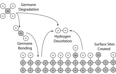
have modelled the deposition process as a dehydrogenation of the germane molecule
which is then added to the surface. Generally, when a precursor breaks down into its
stable compounds it cannot revert to its previous state. When the dehydrogenated
molecule is added to the surface the remaining two hydrogen atoms will then act as
surfactant molecules, covering the surface to prevent dimer bond formation during
the growth. The process is then left with an interchangeable reaction where the two
surfactant hydrogen atoms can then be desorbed to form a hydrogen molecule to
[image:44.595.122.517.339.590.2]leave two free surface sites or vice versa. These reactions are shown pictorially in
Figure 2.3.
Figure 2.3: A diagram showing the different stages of precursor deposition of germane on a Si (001) substrate during epitaxy.
Similar reactions take place when SiH2Cl2
Equation 2.4
is introduced to a Si (001) substrate
surface. These are shown in to Equation 2.7, where Equation 2.4 is the
irreversible breakdown of the precursor gas. Equation 2.5, Equation 2.6 and Equation
GeH4. See Hierlemann et al [25] for the more complicated reactions when both
GeH4 and SiH2Cl2 precursors are mixed for growth of SiGe alloys.
) ( 4 * ) ( * 2 * 2 * 4 ) ( 2
2Cl g H Cl Si b b
SiH + → + + + Equation 2.4
* 2 ) ( ) ( 2 *
2H + b ↔H2 g + Equation 2.5
* 2 ) ( ) ( 2 *
*+H + b ↔HCl g +
Cl Equation 2.6
* 2 ) ( ) ( 2 * ) ( *
2Cl +Si b + b ↔ SiCl2 g + Equation 2.7
The growth rate of precursors generally have two regimes; if the temperature is
relatively low then it is dependent on the temperature applied (temperature limited).
However, when the temperature is relatively high the growth rate is limited by the
ratio of precursor gas flow (mass-flow limited). This is shown in Figure 2.4 by the
comparative SiH2Cl2 and GeH4 growth rate graphs. SiH2Cl2 has a transition
temperature of approximately 960°C and GeH4 of about 400°C. When SiH2Cl2 and
GeH4 are mixed an average growth rate trend is observed, with a different transition
temperature. See Hartmann et al [26] for growth rate information for a mixture of
Figure 2.4: Growth rates as a function of temperature when compared to work performed on SiH4 (silane, Everstey [27]), SiH2Cl2 (Everstey [27]) and GeH4 (Cunningham [28]). Work done
by Cunningham et al was performed within an ultra high vacuum CVD.
HCl gas is one of the gaseous compounds which are created by SiH2Cl2. Hartmann
et al [29] show that an addition of HCl gas to the GeH4 and SiH2Cl2 mixture
decreases the growth rate when grown under low temperatures. Therefore the
temperature of growth must be kept high (> 700°C) to avoid this detrimental effect.
2.2.4 Chamber Etching
Section 4.2 outlines the growth parameters used in this study. Due to the high GeH4
flow and the relatively high growth temperatures SiGe deposition on the quartz wall
of the CVD chamber occurs. Increasing the wall deposition decreases the amount of
IR radiation reaching the substrate which results in a lower growth-temperature. The
delay of the temperature control system and the deposition on the side of the
chamber alters the growth kinetics by lowering the applied growth temperature for a
small period of time. This results in lowering the growth rate and therefore the Ge
contamination during growth [30]. Most importantly, the difference in thermal
expansion between a thick layer of chamber deposition and quartz chamber can crack
the chamber itself [31]. The solution to these problems is a regular etching of the
growth chamber deposition during the growth process itself, whilst taking care not to
etch the wafer. To keep wall deposition within acceptable thicknesses (~1 µm) a HCl
etch step was instigated during the growth of layers. This was performed either
between constant composition layers and the graded region, or at every 1 µm of
growth on the substrate. Etching of the chamber was performed by cooling the
substrate to 400°C, and removing it from the growth chamber. The chamber was kept
under a H2
2.5.4
ambient atmosphere then exposed to an HCl etch. This continual etching
of the chamber during growth provides a thermal cycle to the wafer. This thermal
cycle is thought to induce an extra thermal strain(Section ) and with the addition
of contaminants during growth may produce cracking (Section 2.5.5) of the epitaxial
layer.
2.3 Growth Kinetics of Silicon-Germanium
The growth process is defined as an exchange of molecules from a vapour phase and
adsorbed surface molecules. The surface molecules are then subject to surface
diffusion until incorporated within a substrate lattice site. The kinetics of the growth
process determines the quality of epitaxial layer and how layers are formed.
![Figure 1.1: A graph showing Moore’s law in action by plotting all the commercial transistors’ release date versus the number of transistors per chip [7]](https://thumb-us.123doks.com/thumbv2/123dok_us/9732253.474074/29.595.139.501.347.554/figure-showing-action-plotting-commercial-transistors-release-transistors.webp)

![Figure 1.4: A graph of various semiconductors’ bandgaps and their lattice parameters. Adapted from Veeco[17]](https://thumb-us.123doks.com/thumbv2/123dok_us/9732253.474074/35.595.136.514.101.361/figure-various-semiconductors-bandgaps-lattice-parameters-adapted-veeco.webp)
![Figure 2.4: Growth rates as a function of temperature when compared to work performed on (Cunningham [28])](https://thumb-us.123doks.com/thumbv2/123dok_us/9732253.474074/46.595.163.475.70.277/figure-growth-rates-function-temperature-compared-performed-cunningham.webp)