RESEARCH ARTICLE
ELECTRICAL CHARACTERISATION OF ION-IMPLANTED SEMI-INSULATING INDIUM
PHOSPHIDE AND OPTIMISATION OF RAPID THERMAL ANNEALING
Dr. Srimani P.K.*
1and Smt. Parimala Y.G.
21R & D Division (CS), B.U., DSI, Bangalore, India
2City Engineering College, VTU, Bangalore-78, India
ARTICLE INFO ABSTRACT
Fe-doped semi-insulating InP samples doped with S and S+Si dual implants were characterised for their electrical properties, namely, Hall mobility, electrical activation, carrier concentration and sheet resistivity using Hall effect and Vander Pauw techniques. The samples doped for levels ranging from 5 X 10¹² to 3 x 1015cm-2 and subjected to Rapid Thermal Annealing for
various temperature and time schedules to determine the optimum anneal schedule. Maximum activations of 66% and high electron mobilities of the order of 1100 cm2/Vs were obtained for
the best anneal schedule which was found to be 750 °C for 10 s.
© Copy Right, IJCR, 2011, Academic Journals. All rights reserved
INTRODUCTION
Ion implantation method of doping semiconductors is the most important technique in device fabrication since it provides a controlled method of introducing impurities into semiconductors. Implantation methods find extraordinary applications in microwave and electro-optic devices. Both InP and GaAs are direct band gap materials which make them especially attractive for both opto-electronic devices and for operation at elevated temperatures. The electron effective mass of InP is much less when compared to that of Si which results in higher operating speeds for devices (Sze, 1981). However, studies on InP have not made as rapid a progress as on GaAs, the reasons for which has been the difficulty in growing high purity materials. InP is particularly useful for microwave devices because of its favourable transport properties compared to GaAs. The main objective of the present work was to study the effectiveness of ion implantation doping in InP.
Ion implantation is particularly of interest in compound semiconductors since diffusion doping is difficult. However ion implantation method results in an inherent problem of radiation damage of the semiconductor crystal which consequently results in a loss of crystal structure, electrical and optical properties. The crystal structure can be recovered by suitable heat treatment of the semiconductor surface. Several annealing methods like furnace annealing, pulse annealing, etc have been tried out by various authors (Molnar, 1980; Pearton et al., 1987).
*Corresponding author: [email protected]
Rapid thermal annealing is a method of short duration pulse annealing and is found to result in very good recovery of crystal structure. In compound semiconductors, annealing process is much more complex due to the possibility of dissociation of the semiconductor material (eg. P is volatile in InP) (Pearton et al., 1987). Non-stoichiometric effects can also result where an implanted atom must reside on a particular sub-lattice of the compound in order to be electrically active (Morgan et al., 1981). Dopants like Si which are amphoteric in nature can occupy either In or P site. Ion implanted and annealed semiconductors can be studied to determine the effect on their properties. Techniques like Rutherford Backscattering give quantitative information on the crystal quality. But the predicted Gaussian distribution of implanted impurities will not necessarily be identical to the distribution of the electrically active centers which may be overwhelmed by the side effects of interstitial impurities, precipitate formation, antisite defects and radiation damage. It is desirable therefore to measure the electrical behaviour of implanted layers and determine the depth distribution of electrically active centers. The electrical behaviour of implanted atoms in semiconductors depends on the type of lattice sites available for the implanted atoms and also on the heat-treatment conditions. Conductivity and Hall effect measurements can be used to determine the average carrier concentration of implanted layers and the carrier mobilities. The doping levels achievable in bulk InP during epitaxial growth gives an indication of the highest doping levels that can be anticipated on implanting dopants like S and Si. Maximum n-type concentrations of ~ 10 19 cm-3 have been reported for Ge, Te and Sn and 2-3 x 10 19 cm-3 for Si form
ISSN: 0975-833X
Available online at http://www.journalcra.com
International Journal of Current Research
Vol. 3, Issue, 7, pp.186-191, July, 2011
INTERNATIONAL JOURNAL OF CURRENT RESEARCH
Article History:
Received 2nd
April, 2011 Received in revised form 7th
May, 2011 Accepted 19th
June, 2011 Published online 16th
July 2011
Key words:
liquid phase epitaxy (Astles et al., 1973). Similar concentrations of 2.5 x 10 19 cm-3 have been obtained for Ge, Te and Sn in LPE layers (Rosztoczy et al., 1970). The highest carrier concentrations obtained in the present work compare with these values. For 50 keV, 1x 114 cm-232S implants into Fe doped InP sheet resistivities > 10 Ohm-cm and the highest activations reported were ~10% for room temperature implants annealed at 760ºC, 20 min under H2-PH3 ambient or using
Si3N4 caps. Surface dissociation in InP has been observed at
temperatures > 400ºC (Vaidyanathan et al., 1981; Guha et al.,
1977). This could result in generally higher sheet resistivities and lower mobilities. In the present work implanted InP samples have been annealed in a graphite boat in a N2 ambient
using Rapid thermal annealing method to prevent surface dissociation.
The presence of an excessive amount of Fe in Fe-doped semi-insulating InP or Fe out-diffusion could also lead to partial compensation of the implant. It has been observed through SIMS studies that in either undoped , unimplanted, substrates or in doped substrates iron redistributes during annealing (Gauneau et al., 1985). The works on RTA (Srimani and Parimala, 2011) followed by Rutherford backscattering and channeling has predicted the above result. In the present work, electrical characterisation of ion implanted InP subject to RTA of different time-temperature schedules were carried out. Implantation doses were varied. N-type donor impurities of S and S+Si were used for the studies.
VAN DER PAUW METHOD
The VAN DER PAUW METHOD (Vander Pauw, 1959) is a technique commonly used to measure the electrical characteristics of semiconductors, such as sheet resistivity and Hall Coefficient. It is a powerful tool, due to its ability to accurately measure the properties of a sample of any arbitrary shape, so long as the sample is approximately two-dimensional and the electrodes are placed on its perimeter. One can also assess the doping type, majority carrier concentration and its mobility and the resulting electrical activation.
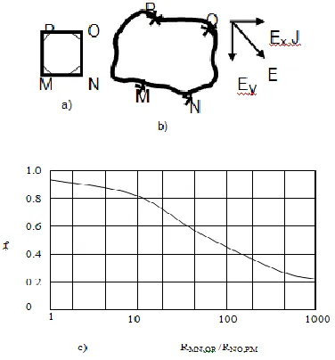
Fig. 1: a) Sample for sheet resistivity measurements with ohmic contacts at the corners; b) An arbitrary shaped sample for sheet resistivity
measurements
In order to use the Van der Pauw method, the sample thickness must be much less than its width and length (Putley, 1960). In order to reduce errors in the calculations, it is preferable that the sample is symmetrical. There must also be no isolated holes within the sample. For accurate measurements four ohmic contacts are placed on the samples such that they are on the boundary of the sample and very small (Figure 1). Leads from the contacts are from the same batch of wires to reduce any thermoelectric effects.
HALL EFFECT
When a magnetic field is applied to a conductor at right angles to the direction of current flow, an electric field is set up in a direction perpendicular to both the current and magnetic field direction. This is known as the HallEffect. A typical sample configuration used for Hall measurements in semiconductors is the Van der Pauw clover leaf pattern (Thomas, 1985). An electric field is applied along the x-axis and a magnetic field along the z-axis. The carriers are subjected to a force Fy which is equal to the Lorentz force evx X Bz. As a result of Fy, an
electric field Ey is produced in the transverse direction. Since
[image:2.612.351.515.316.460.2]there is no net current along the y-direction in the steady state, the Lorentz force on the
Fig. 2. Lorentz Force
electrons (or holes) is balanced by the transverse electric field due to their respective concentrations. This Hall field can be measured externally and is given by
Fy = eEy = evx xBz ………(1)
and since the current density, Jx=nevx
Ey = vY/w=Jx Bz/ne = RHJxBz ……….(2)
where RH is the Hall coefficient and is given by
RH= rH.(p-b2n)/e(p+bn)2 ………(3)
where b = μn/ μp, p and n are the number of holes and number
of electrons and μn and μp refer to the respective drift
mobilities.
If n>>p as in n-type semiconductors, RH=rH(-1/ne) ….(4)
and if p>>n, RH = rH (+1/pe), ……….(5)
rH is called the scattering factor and depends on the dominant
scattering mechanism in the system. It arises because of the fact that the resistance of the material is not totally independent of the magnetic field- some physical magneto-resistance is usually found due to the dependence of the scattering mechanisms on the energy distribution of the
[image:2.612.84.272.494.696.2]electrons. Usually rH is close to unity and therefore the
equation reduces to RH = -1/ne or +1/pe.
Hall mobility
Hall mobility μH is defined as the product of the Hall
coefficient and conductivity
μH =| RH σ| ………..(6)
[image:3.612.89.269.211.403.2]Thus both the carrier concentration and carrier type can be obtained directly from the Hall measurements provided that one type of carrier dominates. Hall mobility can be determined by measuring the Hall coefficient and resistivity.
Fig.3.A schematic of circuit for Hall measurements
[image:3.612.95.242.419.601.2]
Fig. 4. Switch Controller circuit
Sheet resistivity
In practise, the resistivity r, for a sample of arbitrary shape with four contacts on it, as in fig 3 [Van der Pauw,1959], is given by
ρ = πd/2ln2. [RMN,OP + RNO,PM].f ……..(7)
where
RMN,OP = VMN(OP)/IOP(MN) ……..(8)
and RNO,PM = VNO(PM)/IPM(NO) ………(9)
f is a factor which is a function only of the resistance ratio
RMN,OP/RNO,PM. The variation of f with the resistance ratio is
shown in Fig.1.
Hall coefficient
The hall coefficient is obtained from RH = VH w/BI where VH
is the Hall voltage, I is the current , B is the magnetic induction and w is the conductive layer thickness and this will yield the carrier concentration in a uniformly doped semiconductor sample from equation 3. In the present work where the carrier concentration is not uniform with depth, the average carrier concentration have been determined taking conductive layer thickness w = RP + 3ΔRP for S and Si
atoms in InP. The range and range straggling data were estimated from tables (Winterbon, 1975). Several sources of spurious voltages can occur which are eliminated by making a combination of measurements with +B, +I (=V1), -B, +I (+V2),
+B, -I (=V3) and –B, -I (=V4) and we get
VH = (V1 –V2 –V3 +V4)/4 ………(10)
Where VH is the true Hall voltage while the remaining voltages are produced due to other effects such as the Hall probes not being exactly electrically opposite to each other, VM or thermoelectric voltage generated because of an
externally imposed thermal gradient between the probes VT.
VE*, VN* and VRL* are voltages produced due to other effects
and are referred to as the Ettingshausen, Nernst and Righi-Leduc voltages Thus a series of measurements have been made in each case in order to eliminate the effect of any spurious voltages.
ANALYTICAL TECHNIQUES
SHEET RESISTIVITY AND HALL MEASUREMENTS
Samples used for measurements were of square geometry with circular Au-Ge contacts placed at the corners as shown in Fig 1. For accurate measurements using this technique following factors are important: 1.contact configuration is symmetrical 2. Contact is small and at the periphery 3.Contacts are Ohmic 4.Sample thickness is much smaller than the distance between the contacts. A schematic of the measurement circuit is illustrated in Fig 3. A known voltage is applied across precision resistors to generate a current source. The resistors ranged from 1.1 x 10³ to 1.1 x 10¹⁰ Ohms, which produce currents from 9.09 mA to 9.09 nA with a 10 V source. Such low currents were used in order to prevent resistive heating of the samples.
The resistors in the circuit were chosen using a H.P.3488A switch Controller, so as to give a readable output voltage (Vout >1.0mV). The programming model for the switch Controller is shown in fig.4. The output voltage was measured by a Keithley Electrometer, model 619. The gold wires from the sample contacts were soldered on to the current and voltage leads of the circuit. The samples were housed in an enclosed box between the poles of the magnet. The black box was used to avoid photoconductive and photovoltaic effects that could otherwise seriously affect the measurements. For sheet resistivity measurements a current i12 is applied through
between contacts 3 and 4 is measured. Measurements were repeated after switching the direction of current flow. Hall coefficient measurements were performed by applying a current through electrodes 1 and 3 and a magnetic field perpendicular to the plane of the sample. The voltage difference between contacts 2 and 4 was measured. Measurements were again repeated after switching the current directions. The measurements were again repeated after switching the magnetic field direction. A sequence of measurements was carried out in order to overcome the effect of any extraneous voltages.
Formation of ohmic contacts
Contacts formed using 88% Au-12% Ge alloys have been found to be ohmic to n-type InP (A.Piotrowska et al., 1983). The alloy was made in a high temperature furnace by melting the constituents in the ratio 88:12 by weight, in an evacuator and sealed quartz tube. The Au-Ge alloy was e-gun evaporated through a metallic mask, onto the substrate in the pattern shown. The base pressure prior to evaporation was 2 x 10⁻⁷ Torr. The contacts were subsequently alloyed at 440º C for 30 s in the RTA system. Au wires were bonded onto the contacts using an ultra-sonic wire bonder. Assuming the distribution of the implanted atoms to be Gaussian, the carrier concentration averaged over a depth of RP + 3ΔRP was
obtained for various implant doses where RP and Δ RP are
the range and range straggling respectively of the implanted atoms.
N(x)=NPexp-[(x-RP) 2
/2ΔRP 2
] …..(11)
where NP is the maximum value of N(x), i.e., N(RP) and is
given by
NP = φ/(2π)1/2 .ΔRP ………..(12)
where φ is the number of implanted atoms/cm2.
For 60 keV 32S implants into InP, the mean range R P and
relative range straggling ΔRP, estimated from Winterbon
tables are 497À and 287 À respectively. The expected carrier concentrations for various doses of S and S + Si in InP is computed and plotted along with experimental values in Fig. 4. During the electrical measurements, the I-V characteristics of the metal-semiconductor contacts were observed on the implanted samples using a curve-tracer, in order to ensure that the contacts were ohmic.
EXPERIMENTAL DETAILS
Several samples of Fe-doped semi-insulating InP wafer were cut to about 1cm x 1cm using diamond scriber and were initially cleaned using standard cleaning procedures. The samples were doped using ion-implantation techniques under high vacuum using a Freeman ion source (Srimani and Parimala,2011) The samples were doped with S and S+Si dual implants to doses ranging from 5 X 10 12 to 3 X 10 15 atoms /cm2. They were subsequently annealed using Rapid Thermal Annealing for various anneal schedules followed by optical and electrical characterisations using the techniques described, to determine to a first order the ideal anneal schedules for recovering the complete crystal structure and electrical properties.
RESULTS
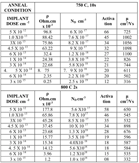
Tables 1 and 2 show the values of the sheet resistivity, carrier concentration, Hall mobility and electrical activation measured for S+ implants of 6 x 1013 cm-2 and 1x1014 cm-2 respectively,
under the different anneal conditions indicated. The typical variations obtained have been indicated through graphs of carrier concentration as functions of implant dose, anneal conditions, electrical activation, mobility and sheet resistivity in figs.5, 6, 7 and 8 respectively. The maximum activation obtained was ~50% for the dose of 6 x 1013 cm-2and ~ 37% for 1 x 1014 cm-2. The highest activation was obtained in both the cases for an anneal of 800 ºC for 10 s. The carrier concentration increases with increasing anneal temperatures while the sheet resistivity and mobility decrease. The variation of ND with anneal temperature is to be expected
because as the anneal temperature is increased residual damage decreases and a greater number of atoms become substitutional and thus carrier concentration increases. The data suggests that better activation can be achieved for even higher anneal temperatures. The instrumental errors during the measurements have been estimated at < 8%. However, for different samples, for the same dose and anneal conditions, there has been a variation of up to 30% in one case (6 x 1013 cm-2 – 750 ºC, 10 s anneal).
Influence of implant dose.
[image:4.612.319.548.461.730.2]The variation of electrical properties with implant dose was studied for three anneal conditions, namely 750º C, 10 S, 800º C, 2s and 800 ºC, 10 s. Fig 8 shows the variation of sheet resistivity with implant dose for various anneal conditions. The variation of mobility with carrier conditions. The variation of mobility with carrier concentration for the 750 ºC and 800 ºC, 10s anneals are shown in the Fig.9.
Table 1. Electrical characteristics after S, S+Si implants and different anneal conditions
ANNEAL CONDITION
750 C, 10s
IMPLANT DOSE cm -2
ρ Ohm.cm
x 10-3
ND cm-3 Activa tion
μ cm2
/Vs
5 X 10 12
96.8 6 X 10 17
66 725
1.0 X10 13
88.42 7.6 X 10 17
45 1002
3X 10 13
75.86 8.2 X 10 17
34 1056
4.5 X 10 13
63.22 9 X 10 17
32 1098
6 X 10 13
32.4 1.2 X 10 18
27 1100
1 X 10 14
24.38 3.8 X 10 18
22 826
3 X 10 14
22.68 5.8 X10 18
21 744
4. 5 X 10 14
8. 75 7. 9 X 10 18
20 611
6 X 10 14
2.35 2.2 X 10 19
20 502
3 x 10 15
0.25 2.5 x 10 19
12 316
800 C 2s
IMPLANT DOSE cm -2
ρ Ohm.cm
x 10-3
ND cm-3 Activa tion
μ cm2/Vs
5 X 10 12
177.8 5.6 X10 17
58 650
1.0 X10 13
65.86 7.8 X 10¹⁷
46 545
3X 10 13
45.28 8.5 X 10 17
35 532
4.5 X 10 13
37.45 10 X 10 17
34 898
6 X 10 13
23.68 1.3 X 10¹⁸
28 676
1 X 10 14
15.77 3.5 X 10 18
19 596
3 X 10 14
15.34 4.0X10 18
18 587
4. 5 X 10 14
14.12 5.6 X10¹⁸
18 584
6 X 10 14
3.96 1.2 X10¹⁸
15 535
3 x 10 15 1.2 1.0 x 10¹⁸ 08 332
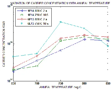
Carrier concentration and electrical activity
In fig 5 the carrier concentrations of the implanted layers are compared to values which represent 100% activation efficiency. Values obtained compare well with other authors (Amithabh Chandra et al., 1980). Fig 5 shows the data obtained for S, Si and S+Si implants. At low implant doses, the carrier concentration increases with ion dose, for all three anneal conditions. A saturation carrier concentration of 3 x 1019 cm-3 appears to be occurring for doses >1015cm-2. For the 750 ºC anneal saturation begins at a higher dose 1 x 1015 cm-2 than for the two high temperature anneals. High carrier concentrations upto 2.5 x 1019 cm-3 have been obtained for this anneals condition at a S implant dose of 3 x 1015 cm-2. On the other hand, for the 800 ºC, 10 s anneal the carrier concentrations are generally higher for low doses, but saturation begins at a much lower dose of ~ 2 x 1014 cm-2. The highest activations were obtained for low implant doses and were 57% for the 750 ºC anneal, 66% for the 800 ºC anneal and 52 % for the 800 ºC 2s anneal (fig 6) . For higher doses the activation generally (~61% for a dose of 5 x 1013 cm-2 compared to 36% for S implant of the same dose. The dual implants of S + Si show a slightly higher activation at the lower dose (~26% at 2 x 1014cm-2 compared to 12% for the S implant). There is very little change for the higher dose. The influence of one or two anneals does not seem to be very significant.
The doping levels achievable in bulk InP during epitaxial growth gives an indication of the highest doping levels that can be anticipated on implanting dopants like S or Si. Carrier concentrations > 1019cm_3 have been obtained in the present work which is comparable with results obtained from LPE InP doped with Ge, Te and Sn (Inada T et al, 1980). The maximum concentrations have been obtained without encapsulation during annealing. Annealing has been carried out in a graphite boat in N2 rich atmosphere to prevent loss of
[image:5.612.337.518.103.241.2]P. Expected electron mobilities of ~ 1100 cm2/V.s. S being a donor impurity, occupies substitutional In site, the dual implantation of S and Si leads to higher activation, particularly at higher doses since the amphoteric Si dopant begins to occupy the P sites as well, acting as an acceptor.
Fig. 5 Variation of carrier concentration with anneal temperature
Sheet resistivity and Hall mobility
[image:5.612.344.517.271.397.2]Low sheet resistivities ~0.25 x 10⁻³ Ohm-cm at 3 x 1015 cm-2 is obtained which decreases with increase in implant dose. High values of resistivities ~ 177 Ohms-cm occur for an anneal at 800 ºC, 2s.
[image:5.612.332.527.351.701.2]Fig. 6. Variation of carrier concentration with implant dose
Fig. 7. Variation of electrical activation with implant dose
Fig. 8. Variation of sheet resistivity with implant dose
[image:5.612.335.524.413.562.2] [image:5.612.79.268.512.667.2]Table2.Variationof carrier concentration with anneal time and temperature for different implant doses of S and S+Si
a) Implant dose 6 x 10 13 cm-2
Theoretical ND 4.2 x 10 18 cm-3
Anneal temp.
Carrier Concentration ND cm
-3
Time 2 s Time 10 s
650 1.8 x 10 17
2.0 x 10 17
700 3.5 x 10 17 2.5 x 10 17
750 6.6 x 10 17
1.2 x 10 18
800 1.3 x 10 18
1.5 x 10 18
850 1.2 x 10 18
1.3 x 10 18
b) Implant dose 1 x 10 14 cm-2
Theoretical ND 6.98 x 10 18 cm-3
Anneal temp.
Carrier Concentration
ND cm
-3
Time 2 s Time 10 s
650 2.3 x 10 17
4.5 x 10 17
700 4.7 x 10 17
5.4 x 10 17
750 1.4 x 10 18
3.8x 10 18
800 1.7 x 10 18
2.6 x 10 18
850 1.5 x 10 18
8.6 x 10 17
CONCLUSIONS
Iron-doped semi-insulating InP samples were implanted with S and S+Si dual implants for varying doses and were thermally annealed using RTA for different time-temperature schedules. They were analysed for their electrical characteristics.
Carrier concentration of implanted atoms saturated at higher doses of implant as expected.
High electrical activations upto 66% and electron mobilities upto 1100cm2/Vs occur for anneal at 750 ºC, 10 s indicative of excellent recovery of crystal structure and electrical characteristics.
Low sheet resistivities were obtained for the above anneal condition
S+Si implants gave better activations for the same anneal conditions
REFERENCES
Amitabh Chandra, Wood, Colin E.C., Woodard, David W. and Eastman, Lester F. 1979. Surface and interface depletion corrections to free carrier density determinations by Hall measurements. Solid State Electronics, Vol.22, p.645-650, 1979
Astles, M.G., Smith., F.G.H.and Williams, E.W. 1973. Indium phosphide, II, Liquid epitaxial growth”, J.Electrochem.
Soc. Solid State Sc. and Tech, Vol.120, No.12, p.1750,
1973
Carter,G., Grant,W.A. 1976. Ion implantation of semi conductors, Wiley, New York.
Davies,D.E., Comer, J.J., Lorenze, J.P. and Ryan, T.G. 1979. “Improved electrical mobilities from implanting InP at elevated temperatures. Appl. Phys. Lett., 15(2).
Donnelly, J.P. 1981. The electrical characteristics of ion implanted compound semiconductors. Nuclear
Instruments and Methods, 182/183, (1981) 553-571.
Gaunneau, M., Chaplain, R., Rupert, A., Coquille, R., Toudic, Y. and Grandpierre, G. 1985. Residual S and Si doping in InP and GaInP. J. Appl. Phys., 57,p4.
Guha, S., and Hasegawa, F., 1977. Effect of heat treatment on n-type bulk grown and VPE InP. Solid-State Electron., (GB), Vol.20., No.1., p.27-28.
Inada, T., Kato S. and Ohkubo T. 1980. Dual species ion implantation in GaAs, Radiation effects,Vol.48, p.91. Moison, J.M. and Bensoussan, M. 1986. Electrical properties
of InP (100) surface. Surface Sci., Vol.168, No.1-3, p.68-73, 1986
Molnar, B., 1980. Close contact annealing of ion implanted GaAs and InP. Applied Phys.Lett., 36(11), 1980
Morgan, D.V., Eisen, F.H., Eris, A. 1981. Prospects for ion bombardment and ion-implantation in GaAs and InP device fabrication”, Review, IEEE Proc., Vol.128, pt.I, No.4.
Pearton, S.J., Poate, J.M., Sette,F., Gibson, J.M., Jacobson, D.C. and Williams, J.S. 1987. Ion implantation in GaAs”, Nuclear Instruments and methods in Physics Research, B19/20: 369-380.
Piotrowska, A., Guivarch, A. and Pelous, G. 1983. Solid State Electronics, Vol.26, No.3, pp.179-197.
Putley, E.H. 1960. Hall effect & related phenomena, Butterworth, London.
Rosztoczy, F.E., Antypas, G.A. and Casau, C.J., 1970. Distribution coefficients of Ge,Sn and Te InP grown by liquid phase epitaxy. Third Int. Symp. On GaAs and
related compounds, Conf. No.9, p.86, Inst. Of Phys.
(1970), London and Bristol.
Srimani P.K. and Parimala, Y.G., 2011.Nano technology approach for the study of RBS & Channeling on ion implantation with computerised data acquisition tools, Proc.of VII International WASET Conference, Malaysia, p.No.954, issue 74.
Sze, 1981. Physics of semiconductor devices, Wiley,N.Y. Thomas, H.,1985. The characterisation of GaAs I – Electrical
techniques”, p.78-104.
Van der Pauw L.J., 1959. A method of measuring the resistivity and Hall coefficient on Lamellae of arbitrary shape, Philips Tech review, Vol.20, p.220, 1959
Vaidyanathan, K.V., Dunlap, H.l. and Anderson, C.L. 1981. Annealing behaviour of Be and four group IV dopants implanted into InP”, Inst. Phys. Conf., Ser. No.63, Chap.8, Int.Symp.on GaAs and related compounds, Japan, 1981
Winterbon, 1975. Ion implantation, Range and Energy deposition distribution, Vol.2, Plenum, New York. Website: www.wikipedia.com