Low Power 32-bit Improved Carry Select
Adder based on MTCMOS Technique
Ch. Mohammad Arif
1, J. Syamuel John
2M. Tech student, Department of Electronics Engineering, VR Siddhartha Engineering College, Vijayawada, A.P, India
Assistant Professor, Department of Electronics Engineering, VR Siddhartha Engineering College, Vijayawada, A.P,
India
ABSTRACT: The raise in requirement for mobile and electronic devices is causing the necessity of low power. This
paper presents the design of Carry Select Adder using MTCMOS technique. A 32-bit CSA is designed. The target technology is Mentor Graphics tool. By utilizing this architecture, power is diminished. This paper shows better results for MTCMOS technique when compared to Improved Carry Select Adder using CMOS and Hybrid Pass Transistor Logic. The comparisons are made between the CMOS logic, Hybrid PTL and MTCMOS. This work is evaluated on the target technology 130-nm Pyxis Schematic Editor.
KEYWORDS: CSA, CMOS logic, Hybrid Pass Transistor Logic, improved CSA, MTCMOS.
I. INTRODUCTION
Area and power reduction are the prominent areas in VLSI system design and data path logic systems. Rapid addition and multiplication have been an initial concern of high performance processors and systems all the time. In digital adders, propagation of carry is the main drawback that affects the speed of addition. The sum is generated continuously for each bit position in a fundamental adder. It is generated only if the preceding bit sum has generated and a carry is propagated into the successive position. The main limitation of the adders is generation and propagation of carry.
Ripple Carry Adder (RCA) includes of cascaded “N” single bit full adders. The carry that is generated as output of the earlier adder becomes the input carry of the next full adder. Hence, the carry of this adder travels the lengthy path. That means if the adder has N stages, it has to travel through N stages. It is the worst case delay path. Fig1 shows the structure of RCA. As the number of stages increments, the delay of adder will also rise in a linear way. RCA is the slowest adder when compared to other adders due to large propagation delay but it consumes less area which is shown in fig.1.
Fig. 1. Ripple Carry Adder
II. LITERATURE SURVEY
Many computational systems use the CSA to balance the problem of carry propagation delay. It produces numerous carries independently and then chooses a carry to provide the sum. However, the CSA is not efficient in terms of area because it employs various pairs of RCA to generate intermediate sum and carry by considering carry input and then the final sum and carry are picked by the multiplexers [1], [2]. To mitigate the above problem, improved CSA is proposed. Here the carry operates as selection line to the multiplexer. Whenever Cin is 0, the sum is calculated by means of XOR operation and Cout is determined by AND operation. Whenever Cin is 1, the sum is computed by means of XNOR operation and the latter is calculated by OR operation.
Carry Select Adder (CSA) is one of the fastest adder and the structure of the CSA displays that there is a chance for improving its efficiency by lowering the power dissipation and area in the CSA. High speed adders are required due to the necessity of high speed and low power computational units in floating point co-processors, image processing units and DSP chips. The most ancient arithmetic operation in processors is addition. The adder is one of the most prominently used computation unit of the processor. Power and delay analysis of various adders and a 32-bit CSA is implemented using Hybrid PTL/CMOS logic style. PTL is considered to be better than static CMOS because it obtains the potential for carrying out a logic function with less number of transistor counts, less delay less power dissipation. The analysis reports discusses that the recommended CSA design displays sophisticated result with respect to area, PDP and power compared to others.
The time required to propagate a carry through the adder is a limitation for the pace of addition in digital adders. In a fundamental adder, the sum for every bit position is provided in order only after the generation of the sum for previous bit position and a carry is propagated into the successive position. The Hybrid PTL/CMOS logic synthesis can develop suitable circuits, taking into account various limitations in the architecture. The multilevel PTL logic cells that are presented, naturally constructed from only a few fundamental cells. In many cases, pure PTL circuits have lesser area and power, but CMOS circuits have shorter delay.
A. Improved Carry Select Adder
It is particularized that output sum (S0) of a single-bit full-adder is XOR of inputs A and B when initial carry is logic „0‟ while output S0 is XNOR of inputs A and B when carry initial is logic „1‟.
when initial carry is logic „1‟. In the similar way the previous carry is used as selection line to second multiplexer so that the carry output of the first stage is selected. It acts as selection line for the multiplexers in the second stage
TABLE1
TRUTH TABLE OF ONE BIT FULL ADDER
Cin A B SUM
(Sout)
CARRY (Cout)
0 0 0 0 0
0 0 1 1 0
0 1 0 1 0
0 1 1 0 1
1 0 0 1 0
1 0 1 0 1
1 1 0 0 1
1 1 1 1 1
B. HYBRID PTL/CMOS logic style
PTL is considered to be better when compared to static CMOS, because it has the capability for carrying out a logic function with less number of transistor counts, delay can be reduced and also power dissipation. Hence PTL is not considered better than CMOS of all kinds of logic structures.
At the circuit level, mixing pass-transistor logic (PTL) with static CMOS has been proposed in a way such that it absorbs less power. In conventional PTL design, committed buffers are introduced in pass transistor trees to bring back driving strength, where as mixed PTL assigns certain number of static gates at optimal points within pass-transistor trees to expand the driving strength as well as performing logic functions.
Fig. 2. Improved Carry Select Adder
impacts the Boolean matching process in the synthesis phase and has a significant impact on the overall quality of the final synthesized results. NMOS-only and PMOS-only pass transistor trees are used in PTL cells to decrease cell size. The complete rail-to-rail swing of the output signal is restored by the extra level-restoring circuit at the output of a PTL gate. The presence of level-restoring circuit at the output of PTL gates not only slows down the PTL gates due to potential drive-fights, but also increases their power consumption. PTL cells are only used for implementing MUX and XOR/XNOR-type logic functions and static gates are used to implement all the remaining logic functions.
III. LOWPOWERCSAUSINGMTCMOS
Multi-Threshold CMOS (MTCMOS) has evolved as an efficient circuit-level technique. Due to this, high performance high performance is achieved. In standby mode, sub threshold leakage can be reduced by turning off the power of the in active blocks by sleep transistors. As CMOS technology is scaled, the supply and threshold voltages are reduced. A steep increase in the sub threshold current arises from the lowering of the threshold voltages. Recently, 40% of the total energy in active mode is dissipated because of leakage currents. As the number of transistors integrated onto the chip, the leakage currents will dominate the total energy consumption in high performance ICs.
MTCMOS technique is one of the prominent techniques. This technique can be used in the reduction of the leakage current. MTCMOS technique operates in two modes, one is the "active" mode and the other is "sleep" mode. The conventional circuit uses single threshold voltage (Vt) while the circuits employing MTCMOS technique uses two different threshold voltages. They are Low threshold and High threshold voltages. These circuits consists of two different types of transistors: the transistor which works on High Vt are known as "sleep" transistors and the transistors which works on Low Vt constitutes the logical circuit. The sleep transistors are used to achieve high performance by reducing the leakage current while the Low Vt transistors improve the circuit‟s speed performance. Even though MTCMOS circuit techniques are efficient, a serious drawback occurs which causes internal nodes to float. As a result, this technique cannot be directly used in standard memory cells without corrupting stored data.
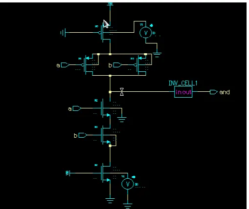
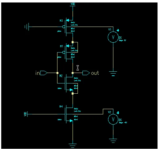
The following figures illustrate the implementation of AND, OR, Inverter and XOR gates using MTCMOS technique. A 32-bit CSA is implemented using this adder based on MTCMOS technique.
The above figure illustrates the implementation of the AND gate and its operation using MTCMOS technique. Design of OR gate using MTCMOS technique is shown in below figure.
Fig. 4. OR gate using MTCMOS technique
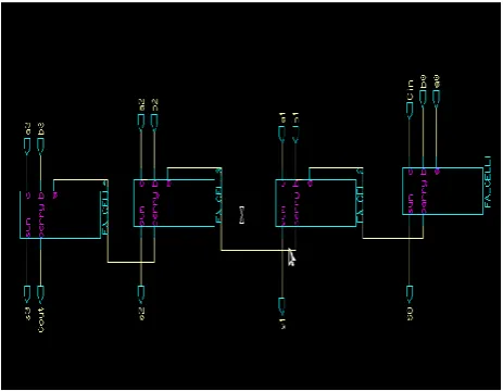
Fig. 6. 32-bit CSA using MTCMOS technique
IV. SIMULATIONRESULTS
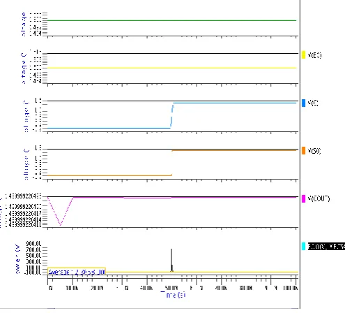
The target technology is the Mentor Graphics Pyxis Schematic Editor 130-nm technology. The fig. 7, fig. 8 demonstrates the 32-bit improved CSA and MTCMOS logic. The results are simulated using this technology and are illustrated as follows.
Fig. 8. Simulation result for 32 bit CSA using MTCMOS technique
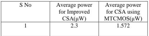
TABLE 1. COMPARISON OF CSAs
S No Average power for Improved
CSA(μW)
Average power for CSA using MTCMOS(μW)
1 2.3 1.572
From the above table it is observed that the average power reduction using MTCMOS Carry Select Adder.
V. CONCLUSION
This paper mainly focuses on the implementation of CSA using MTCMOS technique. The comparison is made between improved CSA and CSA using MTCMOS technique. There is considerable reduction in power dissipated. The designs are evaluated on Pyxis Schematic Editor 130-nm technology.
REFERENCES
[1]Geetanjali Sharma, Lakshay Suri,Student Member IEEE “High Performance and Power Efficient 32-bit Carry Select Adder using Hybrid PTL/CMOS Logic Style”,pp 765-768, 2013 Hybrid PTL/CMOS Logic Style”,pp 765-768, 2013
[2]O.Bedrij,”Carry Select Adder”,IRE trans on Electronic Computers Vol EC-II,pp 340-346.1962.
[3]G. Kishore, P. Sunil Kumar, A. Anil Kumar, “High Speed Carry Select Adder”, IJSRD, Vol. 2, Issue 07, 2014 / ISSN:2321-0613
[4]B. Ramkumar and Hrish M kittur, “Low-Power and Area Efficient Carry Select Adder” in IEEE Transaction on Very Large Scale Integration (VLSI) Systems, Vol.20, No.2, February 2012.
[5]Shen-Fu Hsiao Ming-Yu Tsai, and Chia-Sheng Wen,”Low Area/Power Synthesis using Hybrid Pass Transistor/CMOS Logic Cells in Standard Cell-based Design Environment,” IEEE Trans.Circuits and Systems vol. 57, NO.1, Jan 20
[6] Paanshul Dobriyal, Karna Sharma, Manan Sethi, Geetanjali Sharma,” A High Performance D-Flip Flop Design with Low
Power Clocking System using MTCMOS Technique”, 978-1-4673-4529-3/12/$31.00_c 2012 IEEE.