IMPROVING THE PERFORMANCE OF AN ANTENNA ARRAY BY USING RADAR ABSORBING COVER
A. A. Abdelaziz
Faculty of Engineering
Misr International University (MIU) Cairo, Egypt
Abstract—Improving the performance of a microstrip antenna array has been considered based on the innovative use of an absorbing radar cover.Since the surface wave between antennas array elements plays a major role in mutual coupling and scattering behavior of array antenna. The main objective of this work is to reduce the effect of surface wave between array elements using radar absorbing cover.The absorbing cover has been designed with spatial configuration to get maximum performance at the resonant frequency of the fabricated microstrip antenna array.The measured results of the tested antenna array show a significant reduction of both mutual coupling between array patches and radar cross section of the tested antenna array with minimum side effects on the antenna parameters.
1. INTRODUCTION
significantly to the mutual coupling especially in the E-plane.It has been also reported that [7] surface wave plays a major role in the scattering behavior of antenna arrays.The main goal of this paper is to improve the performance of antenna array by reducing both mutual coupling between MPA and the Radar Cross Section (RCS) of the antenna array.
2. MUTUAL COUPLING BETWEEN ARRAY ANTENNA ELEMENTS
Consider an array of (N) identical elements separated by distance
w1, w2, . . . , wN−1 with element pattern f(θ) and spacing between the (n) and (n+ 1) element iswnwheren= 1,2, . . . , N.Assuming no
mutual coupling, the radiated fieldE is [1]:
E∼f(θ) exp(−jkR)AF(θ) (1) whereAF(θ) is the array factor and is equal to:
AF(θ) =
N
n=1
Vn(0)exp
jk
N−1
i=1
wi
sin(θ)
(2)
and k is the free space wave number and R, θ are the spherical coordinates.
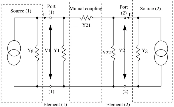
Source (1) Source (2)
Element (1) Element (2)
Port (1)
Port (2)
(1) (2)
Mutual coupling
Yg V1 Y11 Y22 V2 Yg
Y21
I1 I2
For the case of mutual coupling, consider theY-network given in Figure 1 for two identical antenna elements.The actual excited voltage
V1 is equal to the applied voltage V1(0) plus that excited by the mutual coupling and is equal to:
V1 =V1(0)−
Y12
Y11+Yg
V2 (3)
Now, invoking superposition and neglecting higher order coupling:
Vn=Vn(0)− N
m=1
m=n
CmnVn(0) (4)
whereCmn is the mutual coupling factor and is equal to:
Cmn =
Ymn
Ynn+Yg
, Cmm = 0 (5)
where:
Ymn is the mutual admittance between themth andnth elements
Y11 is the self-admittance of the element at the feed terminals
Yg is the generator or feed-line admittance
Now replace Vn(0) in Equation (2) byVn from Equation (4) to include
mutual coupling:
AF(θ) =
N
n=1
Vn(0)exp
jk
N−1
i=1
wi
sin(θ)
− N n=1 N m=1
m=n
CmnVn(0)exp
jk
N−1
i=1
wi
sin(θ)
(6)
3. EFFECT OF MUTUAL COUPLING ON ANTENNA ARRAYS
(or received) by a phased array.Pozar [5] explained the blindness mechanism as a forced surface wave and at scan-blindness, the input impedance of any printed element in the array has a zero real part and a very large reactive part, so the antenna elements are effectively open-circuit.In Equation (6), AF(θ) will decrease sharply if the will add up in phase causing a null in the active element pattern resulting in the so called blind-angle phenomena.On the other side, it has been demonstrated that the surface wave, part of mutual coupling, plays a major role in the scattering behavior of microstrip printed dipoles [5].So, it is very important to compensate the term Cmn of
mutual coupling to improve the antenna array performance.There are many techniques [8–10] to compensate mutual coupling in array antennas with conception of using metal walls between patch elements in array antennas.These metal walls prevent antenna elements from coupling to each other via parallel-plate waveguide modes.A new technique is used based on using Radar Absorbing Material (RAM) cover.
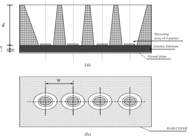
(a)
(b)
Microstrip array of 4 patches
Antenna Substrate
Ground plane
RAM COVER
4. TESTED MICROSTRIP ANTENNA ARRAY CONFIGURATION
The specific array antenna configuration is shown in Figure 2.It is a linear array of 4-circular patch elements with radius = 8.8 mm and separation distance w = 25 mm printed on a plastic substrate of size 100×140 mm and type RT/duroid 5870 with relative permittivityεr =
2.32,t= 34µm andh= 1.58 mm.The measured resonance frequency is equal to 6.12 GHz. The radome cover is an absorbing material, with 4-conical windows, manufactured from sponge loaded with spatial graphite with specified concentration and grain size.By choosing the layer thickness (d= 8 mm) and graphite properties properly, significant absorption characteristic can be achieved.Maximum absorption was adjusted to be at the resonant frequency of the antenna array since a negligible backscatter from the array occurs when the incident frequency is below the fundamental resonant frequency of the MPA elements [11].The measured reflected power in dB from the RAM cover backed by metallic plate was done by swept frequency microwave reflectometer type MWT PR-17 SC and shown in Figure 3.
-20 -15 -10 -5 0
4 5 6 7 8
Frequency (GHz)
R
e
fl
e
cte
d
P
o
w
er
(d
B
)
5. MEASURED PARAMETERS OF THE ANTENNA ARRAY
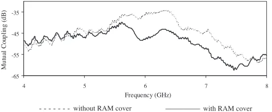
The measured parameters of the antenna array were carried out by the Network Analyzer type HP 8720 D.The measured return loss (S11) and mutual coupling (S21) of the antenna array with and without the RAM cover are given in Figure 4 and 5 respectively.The main parameters of the measured antenna array with and without the RAM cover are summarized in Table 1.
4 5 6 7 8
Frequency (GHz)
R
e
tu
rn
L
o
ss
(d
B
)
-25 -20 -15 -10 -5 0 5
without RAM cover
- - - __with RAM cover
Figure 4. Measured return loss (S11) of the antenna array for two cases.
-65 -55 -45 -35
4 5 6 7 8
Frequency (GHz)
M
u
tu
al
C
o
u
p
li
n
g
(
d
B
)
without RAM cover
- - - __with RAM cover
Figure 5. Measured mutual coupling (S21) of the antenna array for two cases.
Table 1. Size comparison.
frequency
(GHz)
return loss (dB)
mutual coupling (dB)
self impedance ( )
Without RAM cover 6.12 -16.271 -35.669 62.3 + j 11.97
With RAM cover 6.12 -23.653 -46.662 45.1 + j 3.87
Ω
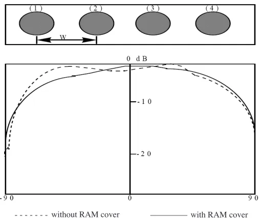
at the resonant frequency.The measured E-plane radiation patterns of the tested antenna at resonant frequency (6.12 GHz) with and without the radome cover are given in Figure 6.The dashed line is the E-plane radiation pattern for the center array element (2 or 3) when all other elements are loaded by 50 Ω impedance and without RAM cover, while the solid line is the measured result when the array elements are with RAM cover.The measured radiation patterns show that the RAM does not affect the pattern, while the inaccuracy of the radiation patterns at the boresight may be due to errors in measuring capabilities.
without RAM cover
- - - __ with RAM cover
without RAM cover
- - - __with RAM cover
-15 -10 -5 0
4 5 6 7 8
Frequency (GHz)
R
e
fl
e
c
te
d
P
o
w
e
r
(d
B
)
Figure 7. Measured reflected power from the tested antenna array for two cases.
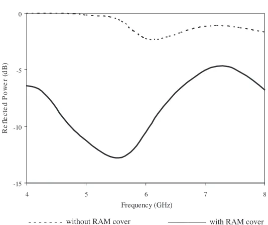
6. RCS REDUCTION OF A MICROSTRIP ANTENNA ARRAY
There are many techniques [12–20] used to reduce the RCS of a microstrip antenna array but with some penalties in radiation efficiency, impedance matching and RCS reduction at the out-of-band frequencies.Most of these penalties have been canceled by the novel technique proposed in this work.The RAM cover with conical holes over the radiating elements is used as shown in the tested antenna configuration given in Figure 2.The measured reflected power from the tested array antenna without and with the radome cover is given in Figure 7.The results show a reduction by 5 to 10 dB over the measured frequency band from 4 to 8 GHz.
7. CONCLUSION
by 10 dB over a wide band of frequencies.Also, the RCS of the antenna array has been reduced by 5 to 10 dB over the whole measured frequencies.On the other side, the radiation pattern or impedance matching has not been affected.
REFERENCES
1. Lo, Y.T.and S.W.Lee,Antenna Handbook Theory, 1st edition, Van Nostrand Reinhold, New York, 1988.
2. Bhattaacharyya, A.K.and L.Shafai, “Surface wave coupling between circular patch antennas,” Electronic Letters, Vol.22, 1198–1200, October 1986.
3.Lechtreck, L.W., “Effects of coupling accumulation in antenna arrays,” IEEE Trans. Ant. Prop., Vol.AP-16, 31–37, January 1968.
4. Krusevac, S., P.B.Rapajic, and R.Kenedy, “Mutual coupling effect on thermal noise in multi-element antenna systems,”PIERS Online, Vol.2, No.1, 2005.
5. Pozar, D.M.and D.H.Schaubert, “Scan blindness in infinite phased arrays of printed dipoles,” IEEE Trans. Ant. Prop., Vol.AP-32, 602–610, June 1984.
6.Dubost, G., “Influence of surface wave upon efficiency and mutual coupling between rectangular microstrip antennas,” Proceeding IEEE International Symposium Digest on Ant. Prop., Vol.2, 660663, Dallas (USA), May 1990.
7. Antilla, G.E.and N.G.Alexopoulos, “Surface wave and related effect on the RCS of microstrip dipoles printed on magneto dielectric substrates,”IEEE Trans. Ant. Prop., Vol.AP-39, 1707– 1715, December 1991.
8. Steyskal, H.and J.S.Herd, “Mutual coupling compensation in small array antennas,”IEEE Trans. Ant. Prop., Vol.AP-38, 1971– 1975, December 1990.
9.Mailloux, R.J., “On the use of metallized cavities in printed slot array with dielectric substrate,”IEEE Trans. Ant. Prop., Vol.AP-35, 477–487, May 1987.
10.Aberle, J.T., “On the use of metallized cavities backing microstrip antennas,” IEEE Ant. Prop. Society Symposium, Vol.1, 60–63, Canada, June 1991.
12.Jackson, D.R., “A multiple-layer radome for reducing the RCS of microstrip patch,” Proceeding IEEE International Symposium Digest on Ant. Prop., Vol.2, 374–377, Dallas (USA), May 1990. 13.Chu, R.S., “Analysis of an infinite phased array of dipole elements with RAM coating on ground plane and covered with layered radome,”IEEE Trans. Ant. Prop., Vol.AP-39, 164–176, February 1991.
14.Pozar, D.M., “RCS reduction for a microstrip antenna using a normally biased ferrite substrate,” IEEE Microwave and Guided Wave Letters, Vol.2, 196–198, 1991.
15.Shimada, K., K, Ishizuka, and M.Tokuda, “A study of RF absorber for anechoic chambers used in the frequency range for power line communication system,”PIERS Online, Vol.2, No.5, 2006.
16.Gustafsson, M., “RCS reduction of integrated antenna arrays with resistive sheets,” Journal of Electromagnetic Waves and Applications, Vol.20, No.1, 27–40, 2006.
17. Zhao, S.C., B.Z.Wang, and Q.Q.He, “Broadband radar cross section reduction of a rectangular patch antenna,” Progress In Electromagnetics Research, PIER 79, 263–275, 2008.
18. Sharm, R., T.Chakravary, S.Bhooshan, and A.B.Bhat-tacharyya, “Design of a novel 3 dB microstrip backward wave cou-pler using defected ground structure,”Progress In Electromagnet-ics Research, PIER 65, 261–273, 2006.
19. Wu, B., B.Li, T.Su, and C.H.Liang, “Equivalent circuit analysis and low pass filter design of split ring resonator DGS,” Journal of Electromagnetic Waves and Applications, Vol.20, No.4, 1943– 1953, 2006.