IJEDR1402229
International Journal of Engineering Development and Research (www.ijedr.org)2734
Hspice Simulation of D Latch and Double Edge
Triggered Flip-Flop Using CNTFET
1
Deepak V. Gohil,
2Mr.Yogesh D. Parmar
Parul Institute of Technology AT Limda, Vadodara, India
________________________________________________________________________________________________________ Abstract- The basic VLSI (Very Large Scale Integration) circuit element is Metal Oxide Semiconductor Field Effect Transistor (MOSFET). Moore’s law states that, design performance improves by reduction in gate length. The gate length reduction is also known as scaling. The continuous scaling of the circuit design will cause issues related to electrical performance of the chip. The device fabrication creates major problems when the geometry reaches to nanometer region. For the same purpose, the researchers have found Carbon Nano-Tubes (CNT) as the new worthy candidate. The design of CNT defines its properties, either metallic conductor or semiconductor. The transistor made from CNT is referred as CNT Field Effect Transistor (CNTFET). In this paper, we have Simulate CNTFETs based D Latch and Double Edge triggered D Flip-Flop using Hspice. Section-1 gives brief introduction of MOSFETs and CNTFETs whereas section-2 describes the detailed properties of CNTFETs and section-3 gives details about CNTFET model. Section-4 describes the detailed description about D Latch and Double Edge Triggered D Flip-Flop with Simulation results. Section-5 summarizes the paper and shows future prospects of CNTFETs’ usage.
Keywords— CNTFET, MOSFET, Chirality, Graphene, I-V characteristic, VTC
________________________________________________________________________________________________________
I. INTRODUCTION
For many years, VLSI chip designers have been using metal-oxide semiconductor field-effect transistors (MOSFETs) as basic circuit elements. Designers have used MOSFET based circuits in their designs because they consume lesser power and are cheaper to fabricate [1-2]. The VLSI designs demands high chip density, high speed and low power. These essentials can be achieved by reducing the size of transistor, a process known as scaling [3]. The continuous scaling of the circuit design gives rise to problems like; short channel effect, power dissipation, leakage current and process variation [2, 5]. As a solution to correct these shortcomings and achieve similar performance; the CNTFET is explored. They can be tailor designed to overcome the difficulties encountered during MOSFET scaling [6]. CNT is manufactured with a sheet of graphene rolled up into a cylindrical structure. The CNT can work as metal or semiconductor, based on how the sheet is rolled up [13]. The graphene rolling is expressed by roll vectors (n, m) values, described in section-3. The CNT based FETs can achieve the performance like traditional MOSFET. Prior to the comparison, one must first assume that the CNTFET resemble their characteristics with MOSFET [5, 14-15]. There are prevailing problems related to the CNTFETs’ manufacturing yield. The MOSFET based technology is matured and hence are not detailed as fabrication aspects but, their electrical characteristics are discussed extensively.
II. CNTFET
Carbon is a Group 14 element that resides above silicon in the Periodic Table. Like silicon and germanium, carbon has four electrons in its valence shell. When carbon atoms are arranged in crystalline structures (composed of hexagonal benzene - like rings), they form a number of allotropes that offer exceptional electrical properties [4, 11]. In their semiconducting forms, this carbon nano-material exhibit room-temperature mobility more than ten times greater than silicon [4]. In addition, they can be scaled to smaller feature sizes than silicon while maintaining their electrical properties [4, 13].
IJEDR1402229
International Journal of Engineering Development and Research (www.ijedr.org)2735
Carbon nanotube (CNT) was discovered by S. Ijima in 1991 [6, 8, 11-12, 13, 17-19]. CNTs are hollow cylinders, composed of one or more concentric layers of carbon atoms (graphene) in a honey comb lattice arrangement [4, 13, 18, 20]. The way in which graphene is rolled is expressed by a pair of indices (n, m) called "chiral vector"[7, 10, 14, 16, 20, 21, 24].9 Where a1 and a2 are unit vectors [4][13].
The figure-1 illustrates the basic construction of CNT from graphene (which look like as honey bees’ area). The CNTFET uses conducting channel of CNT between source and drain regions.
CNTFET Basic Parametric Equations:
The single-walled CNT (SWCNT) is treated as a quasi-1-D quantum wire in this paper. For SWCNT with chirality (n1, n2), the diameter (DCNT) is given by ( = 2.49 Å is the lattice constant) [16, 24, 25].
√
Depending on the shape of the cross-section established by the chiral vector slicing across the hexagonal pattern, nanotubes are classified in one of the three groups as: armchair (n1=n2 and ζ=30º), Zigzag (n2=0 and ζ=0º), and chiral (all other cases) where ζ is the angle between chiral vector and zigzag direction vector. Figure-2 shows all these three types of CNTs [10, 20].
As in [27], (m, l) is the l th substate at the m th subband, km is the wavenumber of the m th subband in the circumferential direction, and kl is the wavenumber of the l th substate in the current-flow direction. It defines the subbands with positive band gap as ―semiconducting subbands,‖ and the subbands with zero or negative band gap as ―metallic subbands.‖ Thus, the band structure of metallic nanotubes can be treated as a summation of the metallic and semiconducting subbands. The wave numbers related with semiconducting subbands are given by,
√
{
The energy of the (m,n) th sub-band, above Ei is
√ √
Figure-2 Metallic and semiconducting CNT
IJEDR1402229
International Journal of Engineering Development and Research (www.ijedr.org)2736
∑ * (
(
)
(
)
)+ ( )
14
Here, k is the Boltzmann constant, T is the temperature in Kelvin, Em,0 is the half band gap of the m-th sub-band, Vch,DSis the Fermi potential differences near source side within the channel, e is the unit electrical charge and Ef is fermi level of doped source/drain nanotube in electron-volt (ev). Tbtbt is defined as the Wentzel–Kramers–Brillouin-like transmission coefficient [27, 28] and it is given by
(
( ⁄ )( )⁄
⁄ ) 15
Where is a fitting parameter, which represents the band-gap narrowing effect under high electrical field [25] [26], F is the electrical field triggering the tunneling process near the drain side junction.
III. DESCRIPTION ABOUT CNTFET MODEL
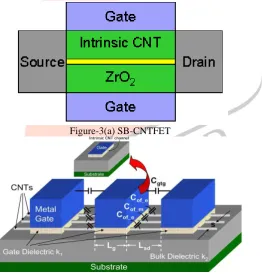
As explained previously, CNTFET can even work as a semi conducting device. There are mainly two types of CNTFET: (a) Schottky barrier CNTFET (SB-CNTFET) and (b) MOSFET like CNTFET. Figure-3(a) shows the structure of SB-CNTFET, where the channel is made up of intrinsic semiconducting CNT in direct metal contact with source and drain regions. The device works on the principle of direct tunneling through the Schottky barrier (SB) at the source-channel junction. The barrier-width is modulated by the application of gate voltage, and hence, the transconductance of the device is controlled by the gate voltage. Figure 3(b) shows three dimensional device structure of MOSFET-like CNFET with multiple channels, high-k gate dielectric material, and related parasitic gate capacitances. It shows three CNFETs are fabricated along one single CNT [31, 32]. The channel region of CNTs is undoped, whereas the other regions of CNTs are heavily doped. The figure-3(b) shows the 3-D device structure of CNFET that is modeled in this paper, with only the intrinsic channel region.
Figure-3(a) SB-CNTFET
Figure-3 (b) three dimensional device structures of CNFETs
This section gives comparison between traditional MOSFET and CNTFET for I-V (P-channel and N-channel) characteristics and Voltage Transfer Characteristics (VTC). The comparison is carried out on the 32nm technology models. The MOSFET and CNTFET HSPICE models are selected from [22] and 32nm BSIM PTM (Predictive Technology Model) Si-MOSFET, respectively. The CNTFET model works for MOSFET like CNFET device. It models voltage controlled current source Ibtbt in order to evaluate the device sub-threshold behaviour and the static power consumption. The expression for Ibtbtis given in earlier section.
IJEDR1402229
International Journal of Engineering Development and Research (www.ijedr.org)2737
IV. DESCRIPTION ABOUT DLATCH AND DOUBLE EDGE TRIGGERED DFLIP-FLOPFigure-4 Circuit Diagram for D Latch
Figure-5 Simulation Results for D Latch Using CNTFET
IJEDR1402229
International Journal of Engineering Development and Research (www.ijedr.org)2738
Figure-7 Simulation Results for Double Edge Triggered Flip-Flop Using CNTFETV. CONCLUSION AND FUTURE WORK
Unipolar, MOSFET like CNTFET model is used to implement digital circuits of D Latch and Double Edge Triggered Flip-flop. This model is used for designing the same digital circuits whose coding has been done in HSPICE; the output waveform is displayed on AvanWaves.
REFERENCES
[1] Xu, Z. H. A. O., W. A. N. G. Yan, and Y. U. Zhi-Ping. "Modeling of Chirality-Dependent Current–Voltage Characteristics of Carbon-Nanotube Field-Effect Transistors." Chinese Physics Letters 23.5 (2006): 1327.
[2] Collier, Natasha, et al. "Application of CNTFETs and MOSFETs circuits at subthreshold." Circuits Team SURI
Program (2003).
[3] Guo, Jing, et al. "Predicted performance advantages of carbon nanotube transistors with doped nanotube as source/drain." arXiv preprint cond-mat/0309039 (2003).
[4] Maneux, Cristell, et al. "Analysis of CNTFET physical compact model." Design and Test of Integrated Systems in
Nanoscale Technology, 2006. DTIS 2006. International Conference on. IEEE, 2006.
[5] Pushkarna, Anuj, Sajna Raghavan, and Hamid Mahmoodi. "Comparison of performance parameters of SRAM designs in 16nm CMOS and CNTFET technologies." SOC Conference (SOCC), 2010 IEEE International. IEEE, 2010.
[6] Ravi, T., and V. Kannan. "Modeling and performance analysis of ballistic carbon nanotube field effect transistor (CNTFET)." Recent Advances in Space Technology Services and Climate Change (RSTSCC), 2010. IEEE, 2010.
[7] Das, Subhajit, Sandip Bhattacharya, and Debaprasad Das. "Modeling of carbon nanotube based device and interconnect using VERILOG-AMS." Advances in Recent Technologies in Communication and Computing (ARTCom 2011), 3rd
International Conference on. IET, 2011.
[8] Sinha, Sanjeet Kumar, Kanhaiya Kumar, and Saurabh Chaudhury. "CNTFET: The emerging post-CMOS device." Signal
Processing and Communication (ICSC), 2013 International Conference on. IEEE, 2013.
[9] Cho, Geunho, Fabrizio Lombardi, and Yong-Bin Kim. "Modelling a CNTFET with Undeposited CNT Defects." Defect
and Fault Tolerance in VLSI Systems (DFT), 2010 IEEE 25th International Symposium on. IEEE, 2010.
[10] Moaiyeri, Mohammad Hossein, et al. "Design and analysis of a high-performance CNTFET-based Full Adder." International Journal of Electronics99.1 (2012): 113-130.
[11] Prabhu, Sameer, and Nisha Sarwade. "Application of CNTFET as Logic Gates and its implementation using HSPICE." [12] Prabhu, Sameer, and Nisha Sarwade. "Hspice Implementation of CNTFET Digital Gates."
[13] Sinha, Sanjeet Kumar, and Saurabh Choudhury. "CNTFET based Logic Circuits: A Brief Review." lJETAE, page (s): 500-504.
[14] Cho, Geunho, and Fabrizio Lombardi. "Delay analysis of gate-adjusted CNTFETs for undeposited CNT defect-tolerance." Nanotechnology (IEEE-NANO), 2011 11th IEEE Conference on. IEEE, 2011.
[15] Roy, Kaushik, Saibal Mukhopadhyay, and Hamid Mahmoodi-Meimand. "Leakage current mechanisms and leakage reduction techniques in deep-submicrometer CMOS circuits." Proceedings of the IEEE 91.2 (2003): 305-327.
[16] Niranjan, Kuldeep, et al. "Comparative Study: MOSFET and CNTFET and the Effect of Length Modulation." International Journal 1.
[17] Yousefi, Reza, Kamyar Saghafi, and Mohammad Kazem Moravvej-Farshi. "Numerical study of lightly doped drain and source carbon nanotube field effect transistors." Electron Devices, IEEE Transactions on 57.4 (2010): 765-771.
[18] Das, Subhajit, Sandip Bhattacharya, and Debaprasad Das. "Design of Digital Logic Circuits using Carbon Nanotube Field Effect Transistors." International Journal of Soft Computing and Engineering 1.6 (2011): 173-178.
[19] Guo, Jing, et al. "Performance analysis and design optimization of near ballistic carbon nanotube field-effect transistors." Electron Devices Meeting, 2004. IEDM Technical Digest. IEEE International. IEEE, 2004.
[20] Bhat, Naagesh S. "Design and modelling of different SRAM's based on CNTFET 32nm technology." arXiv preprint
IJEDR1402229
International Journal of Engineering Development and Research (www.ijedr.org)2739
[21] Marki, Rebiha, Chérifa Azizi, and Mourad Zaabat. "A simple drain current model for carbon nanotube field effecttransistors." Electronics, Communications and Photonics Conference (SIECPC), 2013 Saudi International. IEEE, 2013. [22] J. Deng, ―Device modeling and circuit performance evaluation for nanoscale devices: silicon technology beyond 45 nm
node and carbon nanotube field effect transistors,‖ Doctoral Dissertation, Stanford University, 2007.
[23] Sinha, Sanjeet Kumar, and Saurabh Chaudhury. "Oxide thickness effect on quantum capacitance in single-gate MOSFET and CNTFET devices." India Conference (INDICON), 2012 Annual IEEE. IEEE, 2012.
[24] Fedawy, Mostafa, et al. "IV Characteristics Model for ballistic Single Wall Carbon Nanotube Field Effect Transistors." [25] J. Geist and J. R. Lowney, ―Effect of band-gap narrowing on the built-in electric field in n-type silicon,‖ J. Appl. Phys.,
vol. 52, no. 2, pp. 1121–1123, Feb. 1981.
[26] V. K. Arora and H. Sakaki, ―High-field-induced hot-carrier temperature, bandgap narrowing, and carrier multiplication in bulk semiconductors,‖ in Proc. SPIE—Conf. Physics Technology Semiconductor Devices Integrated Circuits, 1992, vol. 1523, pp. 160–171.