Design and implementation of the DFT using sleep
approach and DTCMOS technique
Thirupataiah Perla & Nalla Swetha Rani
#1Asst. Professor (Dept ECE), Sagar Institute of Technology Hyderabad-India
#2M.TECH,(VLSI&ES), Sagar Institute of Technology Hyderabad-India #1 [email protected]
Abstract:
Design for testability (DFT) refers to hardware design styles or it is an added hardware that reduces test generation complexity and test cost, also increases test quality. Sleep Convention Logic (SCL) is an asynchronous logic style which is based on Null Convention Logic (NCL). In the SCL the combinational blocks are made of threshold gates. Now-a-days the power dissipation is a major problem in electronic devices. The importance for power management Integrated Circuit (PMIC) is emphasized as battery-powered portable electronics such as smart phone are commonly used. Due to this problem static power dissipation is highly increased. In this paper we propose the use of a new DTMOS scheme in DFT Design.
Introduction:
Design for testability (DFT) consists of IC design techniques that add testability features to a hardware product design. The tests are generally driven by test programs that execute using automatic test equipment (ATE) or, in the case of system maintenance, inside the assembled system itself. The diagnostic information can be used to locate the source of the failure. The
DFT method used to test the sleep convention logic. The proposed DFT methodology is based on scan chain design, which is very popular in industry, and it provides for high test coverage. In addition, analysis and development on high potency is crucial to maximize the utilization of moveable device that are most popular numerous functions than within the past. PMIC for prime potency sometimes amendment drastically from linear regulator to switch regulator. however the switch regulator have disadvantage of low potency compared with linear regulator at lightweight load conditions. Therefore, this paper is bestowed the mistreatment of switch regulator at significant load conditions. All power offer device of Mobile appliance should be created stable and numerous DC output voltage of high effectiveness from a unstable DC input power offer. For that reason, it‟s used do an influence offer of Switched Mode Power offer(SMPS) methodology rather than an influence offer of typical linear methodology. Therefore, during this paper, the facility provides are designed mistreatment DT-CMOS that is low on-resistance than CMOS.
SCL_DFT:
SCL is an asynchronous logic style [5] based on theNCL. SCL was originally developed in [6]. SCL combines the idea of the NCL with early completion [7] and fine-grained MTCMOS power-gating [8]. During normal operation, each pipeline stage alternates between set and reset phases. In the set phase, data change from a spacer (called NULL) to aproper codeword (called DATA), and in the reset phase it changes back to NULL. SCL uses delay-insensitive
encoded data for data communication. The most popular delay-insensitive encoding is dual rail. A dual-rail encoded signal D consists of two wires, D0 and D1. D is logic 1 (DATA1) when D1 = 1 and D0 = 0, is logic 0 (DATA0) when D0 = 1 and D1 = 0, and is NULL when both D0 and D1 are 0.Combinational logic blocks in the SCL are made of threshold gates [8] and implement unate functions where no logic inversions are allowed. An SCL gate is generally denoted as THmnWw 1. . . , wn where n is the number of inputs, m is the threshold of the gate, and w1, w2, . . ,wnare the weights of inputs when the weights are > 1.
Fig1:The SCL framework
The SCL framework is shown in Fig. 1. Similar to the NCL, each pipeline stage contains a combinational logic function block (Fi), a register block (Ri), and a completion detector block (CDi).
single gate. Similar to the NCL gates [9], each SCL gate is made of a set block and a hold0 block (denoted as set).In the SCL circuits, however, since all the gates within the combinational blocks are forced to reset by asserting the sleep signal, input-completeness with respect to NULL is inherently ensured and NULL wave front propagation is no longer needed. Transistor-level implementations of rail-0 of a single-bit dual-rail SCL register. This is made of two inverters with a feedback path and can be considered as an unconventional latch. The implementation for rail-1 is exactly the same. Once the sleep signal is asserted, both outputs of the register (i.e., O0 and O1) go to low, producing a NULL value. The outputs remain low until a new DATA value arrives and the sleep signal is deasserted The register outputs will then get asserted according to the DATA value and remain asserted even if the inputs of the register are all deasserted. This latching behavior is special because once an output is asserted by an input it cannot be deasserted by the same input; it only gets deasserted by the sleep signal.
Fig.2 SCL Register
In the SCL completion detector the first logic level is made of the SCL TH12 gates that are essentially similar to Boolean OR
gates; and the subsequent logic levels are made of the SCL THnn gates (where 2 ≤n
≤4) that are essentially similar to n-input Boolean AND gates. Each TH12 gate checks for a DATA value on a single bit of a signaland the THnn gates consolidate the results of a single-bit DATA checks to check for a complete DATA set on the entire signal.Finally, each stage of the SCL pipeline requires a completion C-element. This resettable C-element with inverted output is required to synchronize sleep signals and is critical for a safe DATA/NULL phase alternation; therefore, it must always be active during pipelineoperation and it cannot be put to sleep. In fact, these are the only gates in the SCL pipeline that never sleep.
FAULT ANALYSIS
Faults on Completion C-Element Signals:
A C-element works as follows: the output is asserted when all inputs are asserted; the output remains asserted until all inputs are deasserted (hysteresis behavior). In the SCL, however, this C-element‟s output is inverted. Since in each DATA/NULL phase all inputs and consequently the output of a completion C-element must make a transition for the corresponding DATA/NULL set to propagate through the pipeline.In the SCL pipeline, all stuck-at faults on the inputs and output of all completion C-elements can be detected by allowing a single {DATA, NULL} pair to propagate through the pipeline from primary inputs to primaryoutputs. Therefore, a complete propagation of a {DATA, NULL} pair ensures that there is no stuck-at-0 or stuck-at-1 fault on the inputs and output of completion C-elements.
4.1.2.Faults in Completion Detector:
not stuck-at-1. This is in fact a consequence of using the sleep signal to force the completion detector to get cleared rather than requiring the propagation of a NULL wave front to clear it. Note that if the output of the last gate in the completion detector is stuck-at-1, the pipeline will stall after a while. Stuck-at-0 faults always result in a deadlock, so detecting them is easy. This is due to the fact that all gates within the completion detector must be asserted in the DATA phase toassert the output of the completion detector. Therefore, if even a single transition does not happen due to a stuck-at-0 fault, the output of the completion detector cannot be asserted, which eventually results in deadlock, since the output of the completion detector is an input of the completion C-element.Hence the faults are analyzed by propagating DATA<NULL pair through the pipeline.
4.1.3.Faults in Combinational Logic:
Combinational logic blocks in SCL are unate. In theDATA phase, gates within a combinational block can only make low-to-high transitions; and inthe NULL phase, they can only make high-to-low transitions. This might imply that an approach similar to can be used to detect stuck-at faults inthe combinational logic blocks as discussed earlier; unfortunately, this is not possible for two reasons. The first is that the SCL combinational logic is not input-complete; so, in contrast to the NCL, a stuck-at-0 fault on a signal may not necessarily stop it from producing a valid output DATA set, and hence the pipeline may not stall. The second reason is that a stuck-at-1 fault on the output of a gate may be hidden by the gates at its fanout if those gates can be properly put to sleep. Each combinational logic block in the SCL pipeline behaves exactly like a traditional Boolean combinational logic block when its sleep signal is disabled. Therefore, traditional synchronous combinational ATPG techniques can be used to detectits stuck-at faults.
Faults in Register:
The test patterns generated by traditional ATPG tools are applied to each combinational block through a scan chain design similar to a synchronous approach. This implies that the SCL registers must be augmented to have functionalities similar to a traditional scan cell.
Sleep Signal Fault Analysis
The analysis performed in Section IV-A was based onthe assumption that the sleep signals are fault-free. But in reality, the sleep signals are also prone to stuck-at faults. In this section, the effects of stuck-at faults on sleep signals are analyzed. In the SCL
pipeline, as shown in Fig. 1, each sleep signal generated by the output of a completion C-element is forked to a register block, a combinational logic block, a completion detector block, and the subsequent completion C-element.
Sleep Signal Fork to Registers: A sleep signal that forks to a register block can be either stuck-at-0 or stuck-at-1. In the case of astuck-at-1 fault, the register outputs remain low, causing the register to output NULL at all times. This can be easily detected since no DATA set can then propagate through the pipeline, causing the pipeline to stall. In the case of a stuck-at-0 fault on a sleep signal, the register outputs will never return to NULL once they are set to DATA. When the outputs of registers do not get properly reset by the sleep signal, it will cause the registers tooutput an illegal value. If the new DATA set generates a different output than the previous DATAset then the propagation of illegal values through the pipeline can then be interpreted as a sign of a stuck-at-0 fault on the sleep signal.
Sleep Signal Fork to Completion Detectors:
The sleep signal forks to a completion detector areautomatically tested for stuck-at-1 faults at the time of testing the completion C-elements and are untestable for stuck-at-0 faults due to redundancy.
Sleep Signal Fork to Combinational Logic Blocks:
The stuck-at faults on the sleep signal fork withincombinational blocks are either untestable or it can be ignored due to fault collapsing.
Fault Analysis Summary:
By allowing a single {DATA, NULL} pair to propagatethrough the SCL pipeline, all stuck-at faults on the inputs and output of all completion C-elements can be detected. By disabling the sleep signal, the SCL combinational logic block becomes a normal Boolean circuit that can then be checked for stuck-at faults using the traditional combinational ATPG tools. The stuck-at faults on the sleep signal forks within a combinational logic block are either untestable (stuck-at-0 faults) or can be ignored through faultcollapsing (at-1 faults). The stuck-at faults on the sleep signal forks within a completion detector block are either untestable (stuck-at-0 faults) or can be detected during the test of the completion C-elements (stuck-at-1 faults). The stuck-at faults on the sleep signal forks within a register block are best tested through a scan chain design to be discussed.
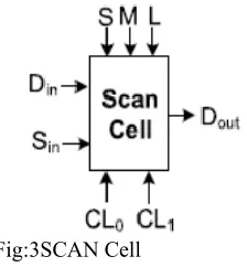
After analyzing different fault scenarios and how they impact the SCL pipeline, we can now devise a methodology to perform testing. •Replacing Registers With Scan Cells: Similar to a synchronous scan-based testing approach, the SCL registers need to be replaced with scan cells in order to shift in the test. Fig. 5 shows the interface of our proposed SCL scan cell.
Fig:3SCAN Cell
In dual-rail encoding, each register bit is made oftwo scan cells, one for each rail. Din is the main input, which could be either rail of a dual-rail input signal. Sin is the scan input, and Dout is the output of the scan cell. In a scan chain configuration, Dout of each scan cell is connected to Sin of the next scan cell. M is the test mode selection signal. When M = 0, the scan cell is in normal mode; but when M = 1, the scan cell enters test mode. In normal mode, the scan cell operates exactly like the SCL register; but in test mode, it behaves like a traditional LSSD-type scan cell, where data can be shifted from Sin to Dout through the non overlapping clock signals CL0 and CL1. In test mode, once the test patterns are applied toa combinational logic block and a sufficient amount of time has passed, the outputs of the combinational logic block can be loaded into scan cells using signal L. Finally, S is the sleep signal that puts the register in sleepmode when the scan cell is in normal mode.
DTCMOS:
Switching loss is fixed cause, but conduction loss by on resistance of switch is increased by a output current increased. When output current is increased, conduction loss is increased more than switching loss in high output current. Finally, switch development that have low on-resistance to heighten efficiency of SMPS is essential.In this paper, we proposed available DT-CMOS without high leakage currents in high power supply voltages using this DT-CMOS‟s concept. The proposed DT-CMOS in this paper can be seen in Fig. 3. When the switch is became ON, the body voltage of the switch MOS is controlled by diode connection CMOS and the threshold voltage is lowered. When the switch is became OFF, body of CMOS is connected to each the power supply and the ground.
Fig:4DTCMOS
isolation from substrate and body to conventional silicon wafer as shown in Fig.4. One-chip of switching device and PFM control circuit are designed by this technique.
Result analysis:
Fig: 5DFT Design
Fig:6DTCMOS based Flipflop
Tabulation:
S.No Vdd=5V Vdd=0v
Sleep
approach 8.321974e-002 watts 7.454881e-002 watts
DTCMOS
1.359866e-003 watts 1.399845e-005 watts
Conclusion:
In paper we propose a new power gating technique with DTCMOS. This DTCMOS method makes the sleep
transistors to operate in high threshold region so that the leakage was reduced. The problem of testing SCL circuits for stuck-at faults was investigated. The faults were initially divided into two separate categories:
1) Faults on logic gates and 2) Faults on sleep signal forks.
The faults within each category were then analyzed separately, and the impact of the faults was discussed. Finally, the proposed DFT methodology was validated through experimental results.
References:
[1]. J. Di and S. C. Smith, “Ultra-low power multi-threshold asynchronous circuit design,” U.S. Patent8 664 977, Mar. 4, 2014. [2] S. C. Smith and J. Di, “Designing asynchronous circuits using NULL convention logic (NCL),” Synth. Lect. Digit. Circuits Syst., vol. 4, no. 1, pp. 1–96, 2009. [3] S. Mutoh, T. Douseki, Y. Matsuya, T. Aoki, S. Shigematsu, andJ. Yamada, “1-V power supply high-speed digital circuit technology with multithreshold-voltage CMOS,” IEEE J. Solid-State Circuits, vol. 30, no. 8, pp. 847–854, Aug. 1995.
[4] P. Lakshmikanthan, K. Sahni, and A. Nunez, “Design of ultra-low power combinational standard library cells using a novel leakage reduction methodology,” in Proc. IEEE Int. SOC Conf., Sep. 2006, pp. 93–94.
[5]P. A. Beerel, R. O. Ozdag, and M. Ferretti, A Designer‟s Guide to Asynchronous VLSI. Cambridge, U.K.: Cambridge Univ. Press, 2010.
power,” J. Low PowerElectron., vol. 4, no. 3, pp. 337–348, 2008.
[7] S. C. Smith, “Speedup of self-timed digital systems using early completion,” in Proc. IEEE Comput. Soc. Annu. Symp. VLSI, Apr. 2002, pp. 98–104.
[8] G. E. Sobelman and K. Fant, “CMOS circuit design of threshold gates with hysteresis,” in Proc. IEEE Int. Symp. Circuits Syst. (ISCAS), vol. 2. May/Jun. 1998, pp. 61–64.
[9] F. A. Parsan and S. C. Smith, “CMOS implementation comparison of NCL gates,” in Proc. IEEE 55th Int. Midwest Symp. CircuitsSyst. (MWSCAS), Aug. 2012, pp. 394–397.
[10] V. Satagopan, B. Bhaskaran, W. K. Al-Assadi, S. C. Smith, and S. Kakarla, “DFT techniques and automation for asynchronous NULL conventional logic circuits,” IEEE Trans. Very Large Scale Integr. (VLSI)Syst., vol. 15, no. 1 0, pp. 1155– 1159, Oct. 2007.
[11] W. K. Al-Assadi and S. Kakarla, “Design for test of asynchronous NULL convention logic (NCL) circuits,” J. Electron. Test., vol. 25, no. 1, pp. 117–126, 2009.
[12] A. Kondratyev, L. Sorensen, and A. Streich, “Testing of asynchronous designs by „inappropriate‟ means. Synchronous approach,” in Proc. 8thInt. Symp. Asynchron. Circuits Syst., Apr. 2002, pp. 171–180.