11
International Journal in Physical and Applied Sciences http://ijmr.net.in, Email: [email protected]THE FEATURES OF CURRENT TRANSMISSION IN LAYERED
GaS(Yb) SINGLE CRYSTALS UPON IRRADIATION WITH
-QUANTA
RAHIM MADATOV1,2, TEYMUR TAGIEV1, AYDAN KHALIQZADEH1,4
1. Institute of Radiation Problems, Azerbaijan National Academy of Sciences, B. Vagabzadeh street 9, АZ 1143, Baku,
2. Azerbaijan National Academy of Aviation, Bina sett., 25th km, Baku, Azerbaijan 3. Baku State University, Vagabzadeh street 9, АZ 1143, Baku, Azerbaijan
The electric and photoelectric properties of GaS<Yb>0.1at% single crystals irradiated with γ-quanta of ≤ 50 krad were studied. It was found that irradiation involves both donor and acceptor defects, in which the vacancy of gallium is dominant. It was found that the increase in electrical conductivity in irradiated crystal at low temperatures is due to the formation of a complex with the participation of an ytterbium atom (~ 0.039 eV), and the quenching of the electrical conductivity in the 200 ÷ 250 K range is due to the formation of a deep donor level with an activation energy of ~ 1.48 eV. It was established that with increasing radiation dose, the depth of quenching decreases and the quenching temperature shifts toward high temperatures.
Key words: Single crystal, semiconductor, photoconductor, defect.
INTRODUCTION
The role and significance of the interaction processes of impurities and defects in the technology of controlling the properties of semiconductor materials is particularly acute in complex semiconductor compounds, which include, in particular, compounds of the AIIIBVI group 1,2,7,8,11. Possessing unique photoelectric, radiation and electro-optical characteristics 3-6,9
, the compounds of this group still do not find proper application in modern devices of optoelectronics because of poor study and complexity of controlling the processes of interaction between impurities and defects in them. The study of the physico-chemical regularities of the processes of restructuring structural defects and impurity-defect interactions in single crystals of AIIIBVI compounds and establishing the interrelation of these processes is an actual task.
In this paper we present the results of studies of the electrical and photoelectric properties of GaS:Yb single crystals irradiated with - quanta in order to determine the effect of the interaction of structural defects with radiation defects on the electrical and photoelectric properties of the layered GaS:Yb.
12
International Journal in Physical and Applied Sciences http://ijmr.net.in, Email: [email protected] EXPERIMENTAL PROCEDURESGrowing of GaS <Yb> (0.1%) single crystals was carried out by directional Bridgman-Stockbarger crystallization. Doping with Yb was carried out during the growth of the single crystal. The obtained crystals had p-type conductivity and their resistivity at the room temperature was 109cm. To create ohmic contacts, indium was used, which was fused to the surface of gallium sulphide at the temperature of 150 °C. Irradiation of samples with - quanta was carried out on a Co60 apparatus at 300 K. The crystals were cooled by pairs of liquid nitrogen upon irradiation, and their temperature did not rise above 290 K. The measurement technique for electrical and photoelectric characteristics of samples was described in12.To measure current in the samples, we used an apparatus assembled on the basis of a universal voltmeter-electrometer V7-30, a microvolt- ampere meter F-136 and a monochromator MS3504i in the temperature range T = 110-300 K and at wavelength λ = 380-800 nm.
RESULTS AND DISCUSSION
The temperature dependence of the electrical conductivity of undoped and doped with rare-earth element Yb (0.1 at%) GaS single crystals before and after γ-ray irradiation has shown at Fig. 1.
It can be seen from the figure that in expressly non-doped GaS crystal (Fig. 1, curve 1), the electrical conductivity in the temperature range T = 130-230 K is almost independent of temperature, and in the region of higher temperatures (T> 230 K) it increases with temperature. In this case, the values of the activation energy of the conductivity found from the slope of the high-temperature branch of the σ (1/T) curve is ~ 1.807 eV, and from the low-temperature part of σ (1/T) curve is ~ 0.015 eV. For the doped GaS(Yb) sample (Fig. 1, curve 2) a straight section with a slope of ~ 0.049 eV is observed on the curve of the electrical conductivity versus temperature. The course of variation of the σ (1/T) in the range from 100 to 300 K shows that in doped samples the carrier concentration in the low-temperature range of 100-210 K decreases, and in the 210-300 K intervals it increases in comparison with the initial samples. A sharp increase in the conductivity in σ (T) at temperatures above ~ 210 K can be explained by the onset of hopping conductivity, which is observed in samples with high defect content15.
13
International Journal in Physical and Applied Sciences http://ijmr.net.in, Email: [email protected] 1.GaS, 2. GaS<Yb>0,1аt%, 3. GaS<Yb>0,1аt%, Dγ=20krad, 4. GaS<Yb>0,1аt%, Dγ=50krad, 5.GaS<Yb>0,1аt%,Е=2,59eV,6.GaS<Yb>0,1аt%, Е=2,3эeV.It should be assumed From Fig. 1, curves 1 and 2, that deep levels with an ionization energy of ~ 1.80 and ~ 1.72 eV exist in the forbidden band of the investigated initial and doped GaS crystals, respectively. As it can be seen from Fig. 1, curves 1 and 2, an increase in the conductivity at T> 200 K in GaS <Yb>0.1 at% crystals is associated with the formation of an acceptor-type level. It can be assumed that the impurities of Yb atoms in GaS form two levels, both acceptor (Ea ~ 1.72 eV) and donor (Ed ~, 049 eV) type, whose concentrations are very different. It can be seen from Fig. 1, curve 3 that after irradiation with gamma quanta in doped GaS <Yb> a decrease in the temperature range of 220-300 K and an increase in conductivity at low temperatures (100-200 K) is observed. As it can be seen from the figure, for the doped samples before and after irradiation (curves 2 and 3), two rectilinear sections corresponding to the levels associated with the presence of Yb (~ 0.049 and ~ 0.039 eV) are observed on the curves. This means that when the crystals of GaS <Yb> are irradiated, an additional level is introduced with the participation of ytterbium. However, it should be noted that the behavior of the electrical conductivity curves in irradiated samples of GaS <Yb> (curve 3, D=20 krad) in the temperature range (200-270 K) differs in comparison with the non-irradiated samples. As it follows from curves 3 and 4, in the region 200-270 K in the irradiated samples of GaS <Yb> quenching of the conductivity is observed, with the increase in the irradiation dose the quenching depth decreases, and also the quenching band shifts to the high-temperature side. It was found that after irradiation of the GaS <Yb>(0.1 at%) crystal with Dγ = 20 and 50 krad (Fig. 1, curves 3 and 4), the value of the activation energy of the impurity conductivity changes with increasing irradiation dose from 0.049 (curve 2) to 0.016 eV (curve 4), respectively. It is seen that in the high-temperature region (T > 200÷230 K), the electrical conductivity of the samples increases with increasing irradiation dose. The calculated activation energy for irradiated samples varies from 1.72 (curve 2) to 1.36 eV (curve 4), which is due to the generation of additional intrinsic charged radiation defects and change in their location in the crystal structures.
To clarify the role and behavior of radiation defects and ytterbium atoms in layered GaS crystals, the influence of illumination (h = 2.59 and 2.3 eV) on the electrical conductivity of the samples was studied. As it can be seen from Fig. 1, curves 5 and 6, when samples are illuminated with monochromatic light, the levels are filled, as a result of which the dependence of the current on temperature is weakened.
14
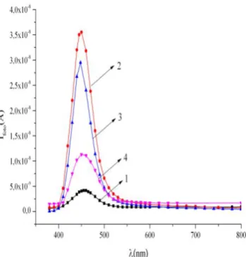
International Journal in Physical and Applied Sciences http://ijmr.net.in, Email: [email protected] 1.GaS, 2.GaS<Yb>0,1аt%, 3. GaS<Yb>0,1аt%, Dγ=20krad, 4. GaS<Yb>0,1аt%, Dγ=50 kradThe spectral distributions of the photoconductivity at room temperature of GaS and GaS<Yb>0.1 at.% crystals before and after irradiation with gamma- quanta are shown in Fig.2. The maximum of photoconductivity is observed near the fundamental absorption edge at λmax= 490 nm (curve 1) in the initial studied crystals. The photoconductivity value at λ=490 nm decreases (curve 2) in crystals doped with ytterbium. After irradiation of the GaS <Yb> at.0.1% crystal, the photoconductivity decreases and the maximum value of the wavelength remains unchanged, but in the impurity region λ = 740 nm the photoconductivity decreases approximately 5 times after irradiation with a dose of Dγ = 50 krad.
The curves of the spectral distribution of the photoconductivity of undoped and yttrium-doped sulphide gallium crystals at T = 110 K, irradiated with γ-quanta of different doses (Dγ = 20 krad, Dγ = 50 krad, Fig. 3) were also registered.
Fig 3. Spectra photoconductivity for the GaS and GaS<Yb>0,1ат% monocrystals at the temperature of Т=110К
1.GaS, 2. GaS<Yb>0,1аt%, 3. GaS<Yb>0,1аt%, Dγ=20 krad, 4. GaS<Yb>0,1аt%, Dγ=50 krad
15
International Journal in Physical and Applied Sciences http://ijmr.net.in, Email: [email protected] are observed with an increase in the irradiation dose (up to 50 krad),. Further, with irradiation the photosensitivity decreases, which is due to an increase in the concentration of recombination centers in the investigated samples, which are chalcogen vacancies. As it is known 3,10,11 layered crystals, in particular GaS, are constructed from layers containing four atomic planes with the arrangement of atoms in the S-Ga-Ga-S layer, each metal is tetrahedrally surrounded by three chalcogen atoms and one metal atoms so that a metal-metal bond is formed. The metal atoms in the structure have a coordination number of 4 sp3-tetrahedral coordination of s2p4 electrons. The sulphide atom has a pyramidal coordination of p3 main s2p4 electrons and a coordination number of 3. The metal-metal bond with the compensation of excess electrons forms the structures of semiconductor bands. The orientation of the bond at the metal atoms gives the chemical bond of these compounds a predominantly covalent character. The negative charge of the metal and the positive charge of the chalcogen are reduced due to the presence of a fraction of the total bond in these compounds. Between the layers, the mutual action is due primarily to forces of the van der Waals type, with a small addition of Coulomb forces.Upon alloying the studied single crystals of gallium sulphide, ytterbium ions due to the relatively small difference in radii between them and the atoms of the metallic component (gallium), can enter both into the natural layers (replacing the Ga vacancies or occupying interstices) and into the interlayer space. Because of this, firstly, the number of vacancy-type structural defects decreases, since the anion atoms taking ytterbium electrons, reduce the hole concentration and secondly, the ytterbium atoms occupying vacancies, being in different layers, form between neighboring layers covalent bonds which are stronger in comparison with Van der Waals bonds. This leads to the healing of structural defects, as a result of which the electrical conductivity of the crystals decreases (Fig. 1, curve 2). And the increase in the electrical conductivity of GaS (Yb) at T> 200 K is due to the creation of a deep level by ytterbium. The electrical conductivity of the crystals is increased at low temperatures (100-200 K) and decreased sharply in the 200-250 K region (Fig. 1, curve 3) when the crystals are irradiated in small doses (30 krad). The observed feature on the (1/T) dependence can be related to the existence of levels 0.037 eV of acceptor and 1.48 eV of donor type, which is due to the formation with participation of initial defects and impurities. It is interesting reduce in the depth of dark current at 200-250 K and shift the minimum to the high-temperature side. This can be caused by a decrease in the concentration of the donor center as a result of the dissociation of the complex with the participation of an impurity atom and a cation vacancy.
16
International Journal in Physical and Applied Sciences http://ijmr.net.in, Email: [email protected] intrinsic region of the spectrum increases, while in the impurity region of the spectrum it decreases at low doses and increases with a further increase in the dose (Figure 3, curves 2.3 and 4). As it can be seen from Fig. 2, at T = 300 K, the photoconductivity of GaS <Yb> samples decreases with increasing irradiation throughout the spectrum. This behavior of the photoconductivity spectra is due to the restructuring of structural defects 5,6,11,15 and impurity-defect effect of irradiation in single crystals of AIIIBVI compounds. This circumstance makes it possible to create a material with predetermined properties and makes it possible to consider gallium sulphide as a promising material for the creation of various devices of electronics and optoelectronics.Thus, the obtained experimental results can be explained in the framework of the model proposed in 1,11,13.
According to this model, gamma-ray irradiation in GaS <Yb> crystals introduces defects of both donor and acceptor types, but assuming that the concentrations of simple defects in the metal and chalcogen sublattices are equal, the main role play defects of the acceptor type (metal vacancies and interstitial chalcogen atoms). With an increase in the dose of γ-irradiation in GaS and GaS (Yb) samples, there is no inversion of the conductivity type, which indicates high concentration of structural defects. These defects are intrinsic structural defects by character and nature. The electrical and photoelectric properties of these crystals are determined mainly by their own electroactive point defects, whose concentration and energy positions of the corresponding levels are determined by technological operations
ACKNOWLEDGEMENTS
17
International Journal in Physical and Applied Sciences http://ijmr.net.in, Email: [email protected] REFERENCES
1. R. S. Madatov, A. I. Najafov, T. B. Tagiev, and A. R. Mobili. Neorganicheskiye Materiali, (2008), p.140-143, 10.1134/S0020168508020039 .
2. R.S. Madatov, T.B. Tagiyev, A.I. Najafov, I.F.Gabulov,Sh.P.Shekili Semiconductor Physics Quantum Electronics Optoelectronics., (2006), p.8-11,.
3. A.I.Najafov, O.Z.Alekperov, L.V. Neorganicheskie Materiali, (1991), p.2432-2433. 4. H.Ertap, T.Baydar, M.Yüksek, M.Karabulut. Turkish Journal of Physic,. (2016), p.297-303, 10.3906/fiz-1604-14.
5. J. V. McCanny and R B Murray.Solid State Physics,( 1977), p.1211-1222.
6. O.Z.Alekperov, M.O.Gogjaev, M.Z.Zarbaliev and R.A.Suleimanov. Solid State Communications, (1991) p.65-67.
7. M. Caraman , V. Chiricenco , L. Leontie , I.I. Rusu .Materials Research Bulletin (2008), p.-3195–3201, 10.1016/j.materresbull.2008.04.014.
8. V. Zolyomi, N. D. Drummond, and V. I. Fal’ko PHYSICAL REVIEW B 87, (2013), p.-195403-1-6, 10.1103/PhysRevB.87.195403.
9. Masanori Ohyama, Hiroshi Ito and Manabu Takeuchi. Japanese Journal of Applied Physics. (2005), p. 4780–4783, 10.1143/JJAP.44.4780.
10. G. Micocci, R. Rella, P. Siciliano, and A.Tepore.. Journal of Applied Physics (1990), p.-138-142, 10.1063/1.347105.
11. H.Kamimura and K.Nakao.Journal of the Physical Society of Japan.(1968), p.-1313-1325.
12. V.Ye. Lashkarev, A.V. Lyubchenko, M.K. Sheynkman. Nonequilibrium processes in semiconductors (Kiyev. Naukova Dumka, 1981).
13. V.S.Vavilov, H.A. Ukhin. Radiation effects in semiconductors and semiconductor devices. M. Atomizdat, (1969), p. 270.
14. V.V.Emchev, T.G.Mashovech. Alloys and defects in semiconductors. M."Radio and Svyazh", (1981), p.247.
15. L.S.Smirnov. Physics prosesses in irradiated semiconductors (red. Smirnov, L.S., Novosibirsk) Nauka, ( 1977), p. 253.