ISSN(Online): 2320-9801
ISSN (Print): 2320-9798
I
nternational
J
ournal of
I
nnovative
R
esearch in
C
omputer
and
C
ommunication
E
ngineering
(An ISO 3297: 2007 Certified Organization)
Vol. 3, Issue 6, June 2015
Study and Analysis of Full Adder in Different
Sub-Micron Technologies with an Area
Efficient Layout of 4-Bit Ripple Carry Adder
Sayan Chatterjee
M.Tech Student [VLSI], Dept. of ECE, Heritage Institute of Technology, Kolkata, WB, India
ABSTRACT: In electronics, adder is an obligatory component of every single integrated circuit. Adder is primary fast and secondly consumed less power and also chip area. We define various adders to perform addition method in VLSI technology. Full adder designing with respect to low power is becoming more popular now adays. It is an essential components of every ALU block. To perform fast arithmetic operations, ripple carry adder is one of the fastest adders used in many data- processing processors. In this paper we analysed a full adder circuit in different sub-micron technologies and obtain low power and minimum delay of it. We also design area efficient layout of full adder schematic. With the help of full adder low power with delay consumed model we design a ripple carry adder schematic and make an area efficient layout of it[1].
KEYWORDS:Low power model, minimum delay, ripple carry adder, Sub- micron technologies and layout.
I. INTRODUCTION
In modern VLSI application adder is used as an arithmetic operations like addition, subtraction, multiplication and division etc. It plays an important role in various digital systems such as microprocessor, microcontroller, DSP processors and data process logic. Full adder and ripple carry adder are the two main parts of adder.
With moving towards ultra sub-micron technology, digital circuits are becoming more complex. Almost every complex circuit needs a full adder circuitry. Several full adder circuits have been proposed targeting on design accents such as power, delay and area. The entire computational block power consumption can be reduced by implementing low power techniques on full adder and ripple carry adder circuitry[2].
In this paper we proposed a full adder circuit as our model. We analyse our model on different sub-micron technologies ( 16nm,22nm,32nm and 45nm) and calculate the delay and power of full adder in each and every sub-micron technology and take an average value of it. Our proposed model has better performance in 16nm technology with the respect of minimum delay and optimum low power use. We make a layout of our model in 45nm technology because it is only available for academic purposes. Using the layout of full adder we design a layout of ripple carry adder which is also on 45 nm technology. Both the layouts are area efficient layout.
The reminder of this paper is divided into five parts. Section II includes some related past work regarding of our paper. Section III describes the theory of full adder and ripple carry adder. Section IV highlighted the schematic of our proposed model and waveform of it. Section V includes analysis of our work with simulation results of power and delay. Section VI includes the layout of full adder and ripple carry adder.
II. RELATED WORK
ISSN(Online): 2320-9801
ISSN (Print): 2320-9798
I
nternational
J
ournal of
I
nnovative
R
esearch in
C
omputer
and
C
ommunication
E
ngineering
(An ISO 3297: 2007 Certified Organization)
Vol. 3, Issue 6, June 2015
types of adder topology like Ripple Carry Adder,Carry Save Adder,Carry Look-Ahead Adder, Carry Increment adder, Carry Skip Adder, Carry Bypass Adder, Carry Select Adder. Author analysis the proposed model in different VLSI parameters and summarised it appropriate manner. Author shows the maximum and minimum power dissipation value in a graphical manner. In [6] author implement different bit of carry look-ahead adder and implement every bit of CLA using VHDL technology. Author describes the detailed VHDL code with graph view in each steps. Author finds CLA occupies less area which considered from the utilization of LUTs, slices and over all gate count and total path delay. In [7] author describes about Designing high-speed, low-power full adder cells based on carbon nanotube technology. Where author focused on different uses of CNT and its application relates with VLSI parameters. Author shows CNT features like high thermal conductivity, high tensile strength,super conductivity, extreme rigidity and be conductor or semiconductor basis on structure those can be an appropriate alternative for CMOS. There is a similarity between CNT and CMOS that’s why author focused to implement a CNT based full adder circuit. In [8] author describes about Low power-area design of 1 bit full adder in cadence virtuoso platform. Where author starts designing 3TXOR gate and tri state inverter model. After that author proposed a 12Tfull adder design incorporates with 3TXOR and tri state invertermodel. Author also proposed 10T,8T,6T full adder circuit and simulate all those models with different VLSI parameter. Author observed that 6T design of full adder has 93.1% power saving compare to conventional 28T design and 80.2% power saving compare to SERF design without much delay degradation. In [9] author describes about full adder cells using static logic, conventional CMOS full adder, full adder using pass transistor logic. Author implement 14T full adder circuit using transmission gate and make a study with delay-power of it. In [10]author implement a high performance 1-bit full adder circuit and implement the delay with respect to given supply voltages.
III.THEORY OF FULL ADDER AND RIPPLE CARRY ADDER
A full adder adds binary number and accounts for values carried in as well as out. A one bit full adder adds three one bit input which are A, B, C_in, where A and B are called operands and C_in is a bit carried in from the next less significant stage. Full adder is a component in a cascade of adder which adds 8,16,32 etc. The output of full adder represent as C_out and S, which are two bit output.
A ripple carry adder usually design by making four full adder block in series. In ripple carry adder, one full adder is responsible for the addition of two binary digits. The carryout of the current stage is fed directly to the carry in on next stage. In this manner ripple carry adder designed[11].
IV.DESIGNING OF TANNER EDA TOOL
ISSN(Online): 2320-9801
ISSN (Print): 2320-9798
I
nternational
J
ournal of
I
nnovative
R
esearch in
C
omputer
and
C
ommunication
E
ngineering
(An ISO 3297: 2007 Certified Organization)
Vol. 3, Issue 6, June 2015
Fig 1. Schematic of full adder
Here two 2-input XOR gate, two 2-input AND gate and one 2-input OR gate are make our full adder circuit design complete. We simulate our proposed model based on the truth table of full adder. The truth table of our proposed model is given as table 1.
Table 1. Truth table of full adder
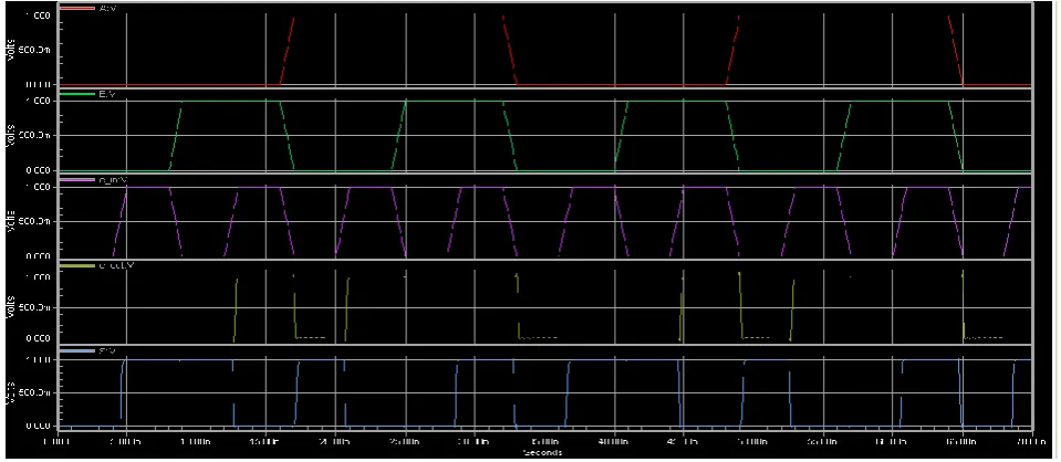
In this truth table we have three inputs are A, B, and C_in and two outputs are Sum and Carry. We generate
input-output graph of our proposed model with respect to the truth table given above. The graph is shown below:-
ISSN(Online): 2320-9801
ISSN (Print): 2320-9798
I
nternational
J
ournal of
I
nnovative
R
esearch in
C
omputer
and
C
ommunication
E
ngineering
(An ISO 3297: 2007 Certified Organization)
Vol. 3, Issue 6, June 2015
We simulate our model in different sub-micron technologies (16nm, 22nm, 32nm and 45nm) and measure the readings of delay and power values. The values are shown on the analysis section as Table 2. Based on the performance of sub-micron technology we design an area efficient layout of our proposed model. Using the full adder circuit block we design a ripple carry adder circuit and make an area efficient layout of it. Both the layouts are include on layout section. The proposed model of ripple carry adder using full adder is given below. Fig 2. Ripple carry adder schematic
Here four full adder join serially and make a ripple carry adder circuit perfect. Every carry out one the current stage is fed as carry in on the next stage, in that way ripple carry adder circuit connected.
V. ANALYSIS
We simulate our proposed model in different sub-micron technology and get the result of delay and power. The values of delay and power are shown below.
Technology Delay(n) Power(Watt)
16nm 6.625 4.6211
22nm 8.945 5.0682
32nm 7.231 4.7690
45nm 6.943 7.7817
Table 2. Delay and power calculation of full adder circuit
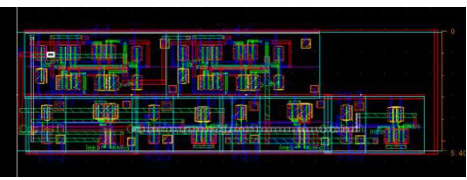
Fig 3.Layout of full adder
ISSN(Online): 2320-9801
ISSN (Print): 2320-9798
I
nternational
J
ournal of
I
nnovative
R
esearch in
C
omputer
and
C
ommunication
E
ngineering
(An ISO 3297: 2007 Certified Organization)
Vol. 3, Issue 6, June 2015
16nm technology where the delay and power value is optimum. In 16nm technology, we have 74% less delay and 91% less power compare to other technologies. This is our low power with high speed proposed model.
VI.LAYOUT OF FULL ADDER AND RIPPLE CARRY ADDER
We develop an area efficient structure of our proposed model which is shown below.
We make this layout using two 2-input XOR gate two 2-input AND gate and one 12-input OR gate. All the gates are connected as our schematic is shown on Fig1. We take 2.5cm as height and 3.5cm as width which is an industry oriented pitch value. We develop our model on cadence virtuoso tool. We used 45nm technology for layout designing because it is easily available on academic purposes. In 45nm technology we achieved second best power-delay result for our proposed model. This is an optimum area efficient layout of full adder. Using the full adder we also develop a ripple carry adder area efficient layout, which is shown as Fig 4.
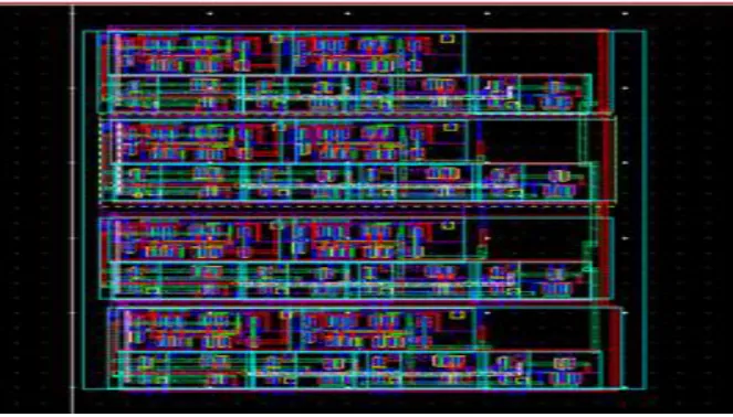
Fig 4. Layout of ripple carry adder using full adder
We create this layout by calling full adder layout cell and connecting the blocks as shown on Fig 2. We take 4.5cm as height and 6.5cm as width value. Those values are making our layout model area efficient. It is also done on cadence virtuoso platform with 45nm technology. This is an area efficient layout of ripple carry adder using four full adder[12].
VII. CONCLUSION
According to the analysis of our model we can conclude that our model is working perfectly on different sub-micron technologies and we take the power-delay values of our model in ache and every sub-sub-micron technology. We have seen that our model has better performance on 16nm technology. It has 74% less delay and 91% less power used respect to other technologies. We also develop an area efficient layout of our proposed model and with the help of this layout we develop a ripple carry adder layout which is also area effective.
REFERENCES
1. Padma Devi, AshimaGirdher and Balwinder Singh, ‘Improved Carry Select Adder with Reduced Area and Low Power Consumption’,
International Journal of Computer Application,Vol 3.No.4, June 2010.
2. Shubhajit Roy Chowdhury, Aritra Banerjee,Aniruddha Roy, HiranmaySaha, ‘A high Speed 8 Transistor Full Adder Design using Novel 3
Transistor XOR Gates’, International Journal of Electrical and Computer Engineering 3:12 2008.
3. S. Knowles, ‘A family of adders’, Proceeding of 15th Symp. Computer Arithmetic, pp. 277–281, Jun. 2001.
4. PallaviSaxena, UrvashiPurohit, Priyanka Joshi, ‘Analysis of Low Power, Area- Efficient and High
Speed Fast Adder’,International Journal of Advanced Research in Computer and Communication Engineering ,Vol. 2, Issue 9,pp.1-3,September 2013.
5. R.UMA,VidyaVijayan, M. Mohanapriya, Sharon Paul, ‘Area, Delay and Power Comparison of Adder Topologies’, International Journal of
ISSN(Online): 2320-9801
ISSN (Print): 2320-9798
I
nternational
J
ournal of
I
nnovative
R
esearch in
C
omputer
and
C
ommunication
E
ngineering
(An ISO 3297: 2007 Certified Organization)
Vol. 3, Issue 6, June 2015
6. Rajender Kumar, SandeepDahiya, ‘Performance Analysis of Different Bit Carry Look Ahead Adder Using VHDL Environment’, International
Journal of Engineering Science and Innovative Technology (IJESIT),Volume 2, Issue 4,pp.1-3,July 2013.
7. Mehdi Masoudi, MiladMazaheri, AliakbarRezaei and KeivanNavi,’Designing high-speed, low-power full adder cells based on carbon nanotube
technology’, International Journal of VLSI design & Communication Systems (VLSICS), Vol.5, No.5,pp.1-2, October 2014.
8. Karthik Reddy. G,’LOW POWER-AREA DESIGNS OF 1BIT FULL ADDER IN CADENCE VIRTUOSO PLATFORM’, International
Journal of VLSI design & Communication Systems (VLSICS) Vol.4, No.4,pp.1-10, August 2013.
9. Manisha, Archana, ‘A COMPARATIVE STUDY OF FULL ADDER USING STATIC CMOS LOGIC STYLE’, Volume: 03 Issue: 06,pp.1-4,
Jun-2014.
10. Hamid Reza Naghizadeh, Mohammad SarvghadMoghadam, SaberIzadpanahTous and Abbas Golmakani, ‘Design of Two High Performance
1-Bit CMOS Full Adder Cells’,Int. J. Com. Dig. Sys. 2, No. 1,pp.1-3, June2013.
11. NeilH.E.Weste, David Money Harris, ’CMOS VLSI design’ , Fourth Edition, Addison-Wesley publication, Boston Columbus Indianapolis
New York San Francisco.
12. Sung-Mo Kang, YousufLeblebici,’CMOS Digital Integrated circuits’, Third Edition, Tata McGraw Hill Education Private Limited, New Delhi.
BIOGRAPHY