A Comparator Circuit Design Using Cyclic
Combinational Gate Diffusion Input (CCGDI) -
For Low Power, Low Area and High Speed
Applications in VLSI Design
G.Sivaiah1,Kanike Vijay Kumar2, T.Kishore3
Assistant Professors, Dept. of ECE, Ravindra College of Engineering for Women, Kurnool, India1,2,3
ABSTRACT: Cyclic Combinational Gate diffusion input (CCGDI) - This technique reduces power consumption, area
and propagation delay of digital combinational circuits while it maintains low complexity of logic design. Performance comparison with traditional CMOS logic design technique is presented with the help of few examples and comparator
KEYWORDS: Cyclic Combinational Gate diffusion input (CCGDI), Double Pass Transistor (DPL), CMOS, Gate
Diffusion Input (GDI), low power design, comparator.
I. INTRODUCTION
Integrated circuit technology is anticipated to scale down through a few more technology nodes, enabling several billion transistors on a single chip. Designs need to trade off among performance and power. The power consumption must be reduced for either of the two different reasons: firstly, to reduce the heat dissipation in order to allow a large density of functions to be incorporated on an IC chip. The other reason is to save energy in battery operated instruments like mobile phones, laptops, palmtops, tablets etc. where average power is in milli watts. In CMOS circuits, the power consumption is proportional to switching activity, capacitive loading and the square of the supply voltage. In order to reduce the power consumption several methodologies have been applied. Several techniques have been introduced to deal with the complexities of low power design like Pass Transistor Logic (PTL), Complementary Pass Logic (CPL), Domino logic, Differential Cascade Voltage Switch (DCVS), MOS Current Mode Logic (MCML), Complementary CMOS (C2MOS), and Double Pass Transistor Logic (DPL) etc. Result shows future CMOS technologies will give an advantage for conventional CMOS circuits in terms of power and speed. Morgenstern, Fish and Wagner introduced a new technique of low-power digital combinatorial circuit design- Gate Diffusion Input (GDI).
As different kinds of logic styles are being introduced, researchers are also involved in developing different algorithms to minimize the logic circuits. Binary Decision Diagrams (BDD) has come to the front as possibly the most successful data formation for representing Boolean functions. After several work researchers rewrite the definition of combinational circuits with cyclic loops, giving noticeable performance improvement.
This paper investigates more on that and explores a new technique for designing of power efficient digital combinational circuit by introducing Gate Diffusion Input (GDI) devices in Cyclic Combinational circuits to overcome the challenges in VLSI design. This new approach Cyclic Combinational Gate diffusion input (CCGDI) has been discussed briefly in section II.
II. BRIEF OVERVIEW OF CCGDI TECHNIQUE
A. Cyclic Combinational (CC) Circuit
Combinational circuits are generally considered as acyclic (i.e., feed-forward) structured. However, cyclic circuits can be combinational. In cyclic combinational circuit the primary outputs is combinational even when some intermediate signals are sequential.
Every digital circuit deals with 0's and 1's. But actually there is no distinct substantial existence of digital signal: each signal is a continuous real valued function of time f(t), related to a voltage level which is actually analog. This can be explained by the given example, extending the set of Boolean values B= [0,1] to the set of ternary values T= [0, 1, ±], where
Logical [f(t)]= 0 if s(t) < Vlow
1 if s(t) > Vhigh
± Unknown
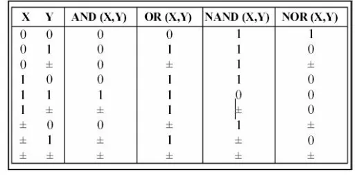
The third value '±' indicates that the signal is in doubt & the value is unknown. We can easily determine the value of circuit output when the input values are either '0' or '1' for any combinational circuit but conventionally we cannot determine the output when value of the one of the inputs is '±' unknown. The truth-tables for the common logic gates
(AND, OR, NAND, NOR gates) including the '±' values are shown in table 1.
TABLE 1: TRUTH TABLE OF COMMON GATES INCLUDING UNKNOWN VALUES
From table 1 it can be seen that for two input gates we can get valid output from different six nos. of combinations of inputs including '±' value. The input combinations where one of the inputs is unknown ('±') but output is either 1 or 0, can be used for making structural feedback in combinational circuit elements. In cyclic design feedback should be such that the primary outputs should be able to give the output as '0' or '1' not '±'. So there is no logical feedback that is transmitted to produce the primary outputs. Thus we can reduce the Boolean expression by introducing extra feedback input without affecting the logical behavior of the circuit. For representing the combinational functions into cyclic circuit, two popular methods are available namely: Branch-and-bound algorithm and Karnaugh map methodology.
B. Gate Diffusion Input (GDI) Technique
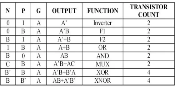
The GDI technique allows realization of a wide variety of complex logic functions using only two transistors. This method is suitable for design of fast, low-power circuits, using a less number of transistors (as compared to CMOS and existing PTL techniques), while improving logic level swing and static power behavior and allowing simple top-down technique by using small cell library. The basic cell of GDI is shown in fig. 1.
1) The GDI cell contains three inputs: G (common gate input of nMOS and pMOS), P (input to the source/drain of pMOS), and N (input to the source/drain of nMOS).
Fig 1. GDI basic cell
TABLE II: VARIOUS LOGIC FUNCTIONS OF GDI CELL FOR DIFFERENT INPUT CONFIGURATION AND CORRESPONDING TRANSISTOR COUNT
Table II shows how different Boolean functions can be realized by simple change of the input configurations of the GDI cell. GDI logic technique consumes less silicon area compared to other logic styles as it consists of less transistor count. In view of the fact that, the area is less, the value of node capacitances will be fewer and for this reason GDI gates have faster operation which presents that GDI logic style as a power efficient way of design.
Our approach of low-power digital combinational circuit design using CCGDI technique includes both the above discussed techniques. The following section describes the methodology of CCGDI technique.
III. CCGDI METHODOLOGY
CCGDI methodology includes two steps, i) General Cyclic representation and ii) GDI realization of cyclic function.
A. General Cyclic Representation
B. GDI realization of cyclic function
Once the cyclic functions are found the next approach is to represent those cyclic Boolean functions with GDI cell. After getting the required CCGDI expressions for the combinational functions the functional and timing analysis is done using standard simulator. For comparative study between CCGDI circuit and conventional CMOS combinational circuit let us take some examples.
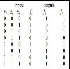
1) Example 1: A set Of three Boolean functions: Here three distinct functions f1,f2 & f3 are taken randomly. The
Boolean expressions and corresponding truth table are as follows:
1 1 2 3 2 1 3
2 1 2 3 1 2 3
3 3 1 2 1 2
(
),
(
),
(
)
,
f
x x x
x x
x
f
x x x
x x
x
f
x x
x
x x
TABLE III: TRUTH TABLE OF FUNCTIONS DESCRIBED IN EXAMPLE 1
To bring cyclic property in the circuit we have listed a dependency between these functions. So a dependency graph can be drawn as fig. 2.
Fig 2. Dependency graph of example 1
So function f1 will be dependent over f2, function f2 will be dependent on f3 & function f3 will be dependent on f1 to
TABLE IV: TRUTH TABLE OF EXAMPLE 1 USING CYCLIC DEPENDENCY
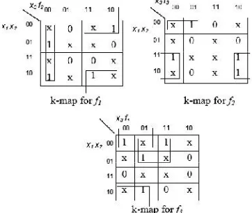
As the no of input variable increases, it gives more flexibility in minimization of Boolean function. The Boolean functions can be derived using k-map. Now k-map representations of cyclic functions f1,f2 & f3 are shown in fig. 3.
Fig 3. K-map representations of f1, f2, f3.
As it can be seen that these k-maps have more nos. of don't care position which implies better flexibility in establishing Boolean functions. So the cyclic solution for the functions f1,f2 & f3 can be represented as:
1 3 2 2 3
2 1 2 3 1 3
3 1 1 2 3
f
x f
x x
f
x x x
x f
f
x f
x x
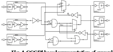
Now cyclic solution for the functions f1,f2 & f3 can be implemented by basic GDI gates using 16 nos. of transistors as
shown below in fig. 4
Fig. 4. CCGDl based representation of example 1.
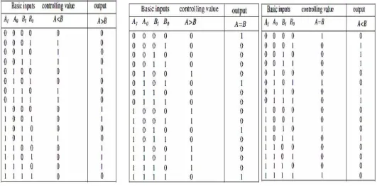
2) Example2: A two bit magnitude comparator can be taken as another example which has four input lines namely
Al & Ao indicating A number and B1 & Bo representing number B. The truth table of a 2- bit comparator is shown in
table V,
TABLE V: TRUTH TABLE OF A 2-BIT COMPARATOR
With the help of k-maps the output functions can be represented as;
1 1 0 0 1 1
1 1 0 0 1 1
1 1 0 0
(
)
(
)
(
)
(
)
(
)
(
).(
)...(1)
A
B
A B
A B B
A
A
B
A B
A B A
B
A
B
A
B
A
B
From this diagram it can be determined that the output A>B is depending over A<B, whereas A=B is depending over A> B and A<B is depending over A =B. Now the truth table can be redrawn as follows;
TABLE VI: TRUTH TABLE OF CYCLIC 2-BIT COMPARATOR
With the help of k-maps the output cyclic functions can be represented as;
1 1 0 0
(
A
B
)
L A B
(
A B
)
, Where L=A<B1 1 0 1 1
(AB)A B EB A( B), Where E=A=B
1 1 0 0 1 0 0
(
A
B
)
A B A
(
B
)
A G A
(
B
)
, Where G=A>B ……….. (2)IV. IMPLEMENTATION OF CCGDI TECHNIQUE
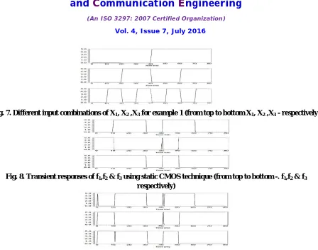
Fig. 7. Different input combinations of X1, X2 ,X3 for example 1 (from top to bottom X1, X2 ,X3 - respectively)
Fig. 8. Transient responses of f1,f2 & f3 using static CMOS technique (from top to bottom -. f1,f2 & f3
respectively)
Fig. 9. Transient responses of f1,f2 & f3 using CCGDl technique (from top to bottom f1,f2 & f3 respectively)
The second example of comparator is simulated for 160ns by providing different input combinations shown in fig. 10. Corresponding transient response of outputs are plotted in fig. 11 and fig. 12 respectively.
Fig. 10. Different input combinations for 2 bit comparator (from top to bottom – A1,Ao, B1, Bo respectively)
Fig. 12. Transient responses of Outputs of two bit comparator using CCGDT technique (from top to bottom - A>B, A<B & A=B respectively)
The third example of seven segment display decoder is also implemented using conventional CMOS technology and proposed CCGDI technique. Both the schematics are simulated for lOOns by providing different inputs Corresponding transient responses of outputs
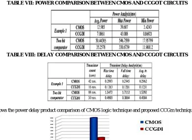
From the simulation results it can be easily understood that the proposed CCGm based circuits have the same logical behaviour as like the conventional CMOS based circuits where as the power & timing behaviours are improved as tabulated in the table VII & VIII,
TABLE VII: POWER COMPARISON BETWEEN CMOS AND CCGOT CIRCUITS
TABLE VIII: DELAY COMPARISON BETWEEN CMOS AND CCGOT CIRCUITS
Fig. 13 shows the power delay product comparison of CMOS logic technique and proposed CCGm technique.
Fig. 13. Power-Delay Product Comparison of different examples described in sec. III
V. CONCLUSION
for more complex functions reduction rate is more. It turns out that in contrast to older process technologies, this approach is more suitable for industrial usage in advanced process technologies.
REFERENCES
[I] A. M. Shams, T. K. Darwish and M. A. Bayoumi. "Permormance Analysis of Low Power I-Bit CMOS full adder cells", IEEE Transaction on VLSI Systems, Vol. 10, Feb. 2002.
[2] Michael Keating, David Flynn, Robert Aitken, Ala Gibsons and Kaijian Shi, "Low Power Methodology Manual for System on Chip Design", Springer Publications, New York, 2007.
[3] Mohamed W. Allam, "New Methodologies for Low-Power HighPerformance Digital VLSI Design", PhD. Thesis, University of Waterloo, Ontario, Canada, 2000
[4] A.Bazzazi and B. Eskafi, "Design and Implementation of Full Adder Cell with the GOT Technique Based on 0.18Jlm CMOS Technology", International MultiConference of Engineers and Computer Scientists (IMES) Vol ll, March 17 - 19, 2010, Hong Kong
[5] Arkadiy Morgenshtein, Alexander Fish, and Israel A. Wagner, "GateDiffusion Input (GOT): A Power-Efficient Method for Digital Combinatorial Circuits", IEEE Transaction on VLSI Systems, Vol. 10, No. 5,pp. 566-581, October 2002
[6] R. E. Bryant, "Graph-Based Algorithms for Boolean Function Manipulation", IEEE Trans. Computers, Vol. C-35, No. 6, pp. 677-691, 1986. [7] Sharad Malik (Dept. of Electrical Eng., Princeton Univ.), "Analysis of Cyclic Combinational Circuits", page: 619,lEEE transaction on computer, 1063-6757/93,1993,
[8] Marc D. Riedel, "Cyclic Combinational Circuits", PhD. Thesis California Institute of Technology, Pasadena, California, 2004, page - 75-87 [9] Marc D. Riedel & Jehoshua Bruck , 'The Synthesis of Cyclic Combinational Circuits" Supported in part by the "Alpha Project" at the Center for Genomic Experimentation and Computation, a National Institutes of Health Center of excellence in Genomic Sciences, DAC, June 2-6, 2003, Anaheim, California, USA. Page 163
[10] Biswarup Mukherjee & Dr. Anup Kumar Dandapat, "Design of Combinational Circuits by Cyclic Combinational Method for Low Power VLSI", International Symposium on Electronic System Design, Bhubaneswar, 2010, pp-I07-112
BIOGRAPHY
Mr. G.SIVAIAH received his B.Tech degree in Electronics and Communication Engineering
from VCE HYDERABAD, JNTU HYDERABAD, A.P. in the year 2006, and M.Tech. Post Graduate in VLSI SYSTEM DESIGN in AITS,RAJAM PET, KADAPA, JNTU Anantapur, A.P. in 2008.Currently He is working as Assistant Professor in Ravindra College of Engineering for Women, Kurnool, A.P., India. He published Seven technical papers in various International journal and National conferences. His current research interests include VLSI DESIGN, Digital Circuits Design
Mr. KANIKE VIJAY KUMAR received his B.Tech degree in Electronics and
Communication Engineering from SJCET College yemmiganur, JNTU Ananthapuramu, A.P. in the year 2009, and M.Tech. Post Graduate in Communication and Signal Processing in GPREC, Kurnool, JNTU Anantapur, A.P. in 2012.Currently He is working as Assistant Professor in Ravindra College of Engineering for Women, Kurnool, A.P., India. He published Seven technical papers in various International journal and National conferences. His current research interests include signal processing, Communication, Digital Image Processing.
Mr. T.KISHORE received his B.Tech degree in Electronics and Communication Engineering