Corresponding Author: Parshang Khorramdel, Department of Atomic and Molecular Physics, Science and research
An Investigation About Optical Parameters Of Silicon Thin Layers As A Function Of
Thickness
1Parshang Khorramdel, 2Mohamad Reza Behfuruz
1Department of Atomic and Molecular Physics, Science and research branch, Eslamic Azad
University, Tabriz, Iran
2Department of Atomic and Molecular Physics, Faculty of science, Eslamic Azad University,
Mahabad, Iran
Abstract: Silicon thin layers were deposited on glass substrates with three different 98 nm, 143 nm and 187 nm thicknesses, under UHV conditions at room temperature. Other deposition conditions were the same for all layers. By using spectrophotometer the Reflectance and the Transmittance of produced layers were obtained. By using Kramers- Kronig method on reflectivity curves other optical parameters such as, real and imaginary part of refractive index, real and imaginary part of dielectric constant, real and imaginary part of conductivity, absorption coefficient and optical band gap energy were calculated. The relation between silicon thickness and optical parameters were investigated and there was a good agreement between them.
Key words: silicon; spectrophotometer; thin layer.
INTRODUCTION
Knowledge on the dependence of optical constants of a material on the wavelength is very essential in obtaining fundamental information on its optical behavior in relation to its electronic transition. This is important in the application of the material in devices (Tong, G.B., et al., 2011). The chemical and physical properties of thin film can be different from bulk properties of the respective materials. These film characteristics are thickness dependent and are controlled by the deposition methods. Recent studies also indicate that refractive index of thin films is thickness dependent and the film thickness is responsible for the optical loss (Zhou, H., et al., 2002). Silicon is non-toxic, relatively inexpensive (silicon comprises about 26% of the earth’s crust which makes it second in abundance only to oxygen), easy to process (a very well established industrial infrastructure in silicon processing exists around the world), and has quite good mechanical properties (strength, hardness, thermal conductivity, etc.) (Adam, A., et al., 2009). Silicon thin films are used in different technological areas such as photovoltaic cells, thin-film transistors, microelectromechanical systems, and Li-ion rechargeable batteries. Silicon dielectrics are important materials for both microelectronics and integrated optics. They have been considered as an appropriate material for fabricating optical waveguides in broadband communications (telecom and datacom) (Mohamed, S.H., et al., 2011). Silicon is very important material in electronics market, dominating the microelectronics industry with about 90% of all semiconductor devices sold worldwide being silicon based (Adam, A., et al., 2009). Currently, the vast majority of flash-memory devices are charge storage based, fabricated in CMOS technology. Because of the increasing demand for information storage, memory device developers and manufacturers are constantly attempting to increase storage capacity for memory devices (e.g., increase storage per die or chip). Silicon-based devices are approaching their fundamental physical size limits (Dima, A., et al., 2008). For several years, hydrogenated silicon (Si:H) has been used commercially as the active sensing layer in resistive uncooled microbolometer imaging arrays in the infrared spectral range. Si:H has been a subject of wide interest for thin film transistors and photovoltaic devices (Saint John, D.B., et al., 2011). Hydrogenated amorphous Silicon (a-Si-H) is one of the most attractive semiconductor materials for the elaboration of thin, flexible and cheap solar cell devices (Barhdadi, A., et al., 2009). The aim of this work is to study the relation between optical properties of silicon thin films and their thicknesses. It has been proven that the film thickness represents very important factor that determines the optical constants.
Experimental Details:
Aust. J. Basic & Appl. Sci., 7(6): 65-71, 2013
techniques. Aspens & Thee’ten’s (Aspnes, D.E. and J.B. Thee'ten, 1980) data for bulk silicon were added to calculated results for comparison.
RESULTS AND DISCUSSION
In this work Kramers- Kronig relations were used to calculate the phase angle θ (E) (Kangarloo, H., et al., 2010):
0 n 1 n 2 2 2 2 2 E0 2 02
0 ) 1 n 2 ]( ) E E ( 4 [ 1 E E E E ln ] ) E ( R ) E ( R ln[ 2 1 dE E E ) E ( R ln ) E ( R ln E ) E ( 2 (1) where E denotes the photon energy, E2 the asymptotic limitation of the free-electron energy, and R(E) the reflectance. Hence, if E2 is known, the θ (E) can be calculated. Then the real and imaginary parts of the refractive index were calculated, from which other parameters were obtained.
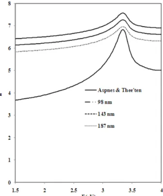
Figure 1 shows real parts of refractive index for the layers produced in this work with different thicknesses of 98 nm, 143 nm and 187 nm and other same deposition conditions. Aspnes&Thee´ten (Aspnes, D.E. and J.B. Thee'ten, 1980) data are also included for comparison. The general trend of our results are the same as Aspnes&Thee´ten (Aspnes, D.E. and J.B. Thee'ten, 1980). There is a peak at 3.4 eV energy for all layers. This peak for Aspnes&Thee´ten (Aspnes, D.E. and J.B. Thee'ten, 1980) result is sharper; which for our results is wide and short.
As long as it can be seen from figure 1, by increasing thickness real part of refracting layers with silicon grains and filling up the voids. There for configuration homogeneous layers.
Figure 2 shows the imaginary part of refractive index. Aspnes&Thee´ten (Aspnes, D.E. and J.B. Thee'ten, 1980) data are also included for comparison. There is a peak at about 3.5 eV energy for all layers. As long as it can be seen from figure 2 by increasing thickness, imaginary part of refractive index increases that is because of filling voids with silicon grains, there for transmittance decreases and absorbance increases.
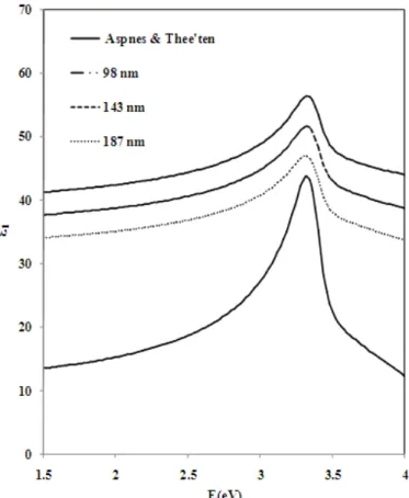
Figure 3 shows the real part of dielectric constant. Aspnes&Thee´ten (Aspnes, D.E. and J.B. Thee'ten, 1980) data are also included for comparison. The general trends of our results are same with Aspnes&Thee´ten (Aspnes, D.E. and J.B. Thee'ten, 1980). There is a peak at 3.4 eV energy for all layers that is sharp and tall for Aspnes&Thee´ten (Aspnes, D.E. and J.B. Thee'ten, 1980), wide and short.
For our results, as it can be seen from figure 3, by increasing thickness real part of dielectric cons that decreases. That is because of formation more metallic layers by increasing thickness also for thicker layers the effect of substrate are also observed.
Figure 4, shows the imaginary parts of dielectric constant, Aspnes&Thee´ten (Aspnes, D.E. and J.B. Thee'ten, 1980) data are also included for comparison. The general trend of our results is same with Aspnes&Thee´ten [9].
There is a peak at 3.5 eV energy for all layers. As it can be seen from figure 4, by increasing thickness, imaginary part of refractive index increases, that depends to more absorbance.
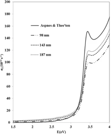
Figure 5 shows, the real part of conductivity index. Aspnes&Thee´ten (Aspnes, D.E. and J.B. Thee'ten, 1980) data are also included for comparison. The general trend and the peak at 3.4 eV energy are the same for all layers.
As it can be seen from figure 5, by increasing thickness, real part of conductivity index increases, that is because of formation completed metallic silicon layers and that is in agreement with figure 3 (real part of dielectric constant). Figure 6 shows, the imaginary part of conductivity index. The general trend of our results is the same with Aspnes&Thee´ten (Aspnes, D.E. and J.B. Thee'ten, 1980) results. The peak is at 3.4 eV energy for all layers, sharp and tall for Aspnes&Thee´ten (Aspnes, D.E. and J.B. Thee'ten, 1980), wide and sharp for our results.
By increasing thickness, imaginary part of conductivity index decreases that depend to absorbance as we discussed before.
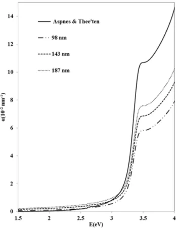
Figure 7 shows, absorption coefficient for the layers produced in this work. Aspnes&Thee´ten (Aspnes, D.E. and J.B. Thee'ten, 1980) data are also included for comparison. The general trend of all layers is the same. The peak at 3.4 eV is shown already. By increasing thickness absorption coefficient increases. That is because of formation of completed layers and filling up the voids with silicon metallic grains, there for transmittance decreases and absorbance increases.
Fig. 1: The real part of refractive index of the layers with different thicknesses.
Aust. J. Basic & Appl. Sci., 7(6): 65-71, 2013
Fig. 3: The real part of dielectric constant of the layers with different thicknesses.
Fig. 5: The real part of conductivity index of the layers with different thicknesses.
Aust. J. Basic & Appl. Sci., 7(6): 65-71, 2013
Fig. 7: Absorption coefficient of the layers with different thicknesses.
Summery:
Silicon thin layers were deposited on glass substrates, under high vacuum condition, At room temperature (300K) with three different thicknesses. Deposition angle was near normal and deposition rates were the same for all layers. By using Kramers-Kronig relations for reflectivity curves, optical constants calculated. By increasing thickness real part of refractive index decreases and imaginary
Parts of refractive index increases that was because of formation more completed layers and filling up the voids, that trends to decreasing transmittance and increasing absorbance. By increasing thickness real part of dielectric constant decreases and imaginary part of dielectric constant increases, for the same reasons there is an increasing and decreasing trend for real part and imaginary parts of conductivity constant respectively. Absorption coefficient increases and band gap energy decreases by increasing thickness that we discussed before.
REFERENCES
Adam, A., Filios, Yeong S. Ryu and Kamal Shahrabi, 2009. Optical Properties and Applications of Nanoscale Silicon, the Technology Interface Journal/Winter Special Issue, selected paper from the Proceedings of the IAJC-IJME 2008 ConferenceVolume 10 No. 2.
Aspnes, D.E. and J.B. Thee'ten, 1980. J. Electrochem. Soc., 127: 1359 D. E. Aspnes and J. B. Theeten, private communication
Barhdadi, A., S. Karbal, N. M’gafad and B.M. Aka, 2009. Optical characterization of a-Si:H thin films grown by Hg-Photo-CVD, M. J. CONDENSED MATTER 11.
Dima, A., F.G. Della Corte, C.J. Williams, K.G. Watkins, G. Dearden, N. O’Hare, M. Casalino, I. Rendina and M. Dima, 2008. Silicon nano-particles in SiO2 sol–gel film for nano-crystal memory device applications, Microelectronics Journal, 39: 768-770.
Kangarloo, H., S. Rafizadeh and B. Salimi, 2010. Optical properties of titanium oxide nano layers. Proc. 3rd WSEAS Int. Conf. on Eng. Mechanics, Structures, and Eng. Geology (EMESEG'10), World Scientific and Engineering Academy and Society (WSEAS), Stevens Point, Wisconsin, USA (Latest Trends on Engineering Mechanics, Structures, Engineering Geology). pp: 305-309.
Mohamed, S.H., M. Raaif, A.M. Abd El-Rahman and E.R. Shaaban, 2011. Properties of Rf Plasma Nitrided Silicon Thin Films at Different Rf Plasma Processing Powers, ACTA PHYSICA POLONICA A, 120: 552-557.
Saint John, D.B., H.-B. Shin, M.-Y. Lee, S.K. Ajmera, A.J. Syllaios, E.C. Dickey, T.N. Jackson and N.J. Podraza, 2011. Influence of microstructure and composition on hydrogenated silicon thin film properties for uncooled microbolometer applications, JOURNAL OF APPLIED PHYSICS 110: 033714.
Tong, G.B., M.R. Muhamad and S.A. Rahman, 2011. Optical Constants and Electronic Transition in Hydrogenated Silicon (Si:H) Thin Films Deposited by Layer-by-Layer (LBL) Deposition Technique, Sains Malaysiana, 40(1): 59-62.