Research Article
a
April
2018
Special Issue: National Conference on Emerging Trends in Engineering 2018
Conference Held at Sri Venkatesa Perumal College of Engineering & Technology, Puttur, A.P., India
International Journals of Advanced Research in
Computer Science and Software Engineering
ISSN: 2277-128X (Volume-8, Issue-4)
A Novel Multi Input Three-Level DC-DC Boost Converter
Chintala Venkatesh
Assistant Professor, Department of Electrical and Electronics Engineering, SMK FOMRA Institute of
Technology, Chennai, Tamil Nadu, India
Dr Y. Sukhi.
Professor, Department of Electrical and Electronics Engineering, R.M.K Engineering College,
Chennai, Tamil Nadu, India
Abstract— Power electronics solutions based on multiple converter configurations offer cost-effective solutions by integrating a number of components at input or output power stages. This paper proposes a new multi input isolated three-level converter for renewable and sustainable energy systems adopting high dc link voltage. Multiple dc sources are integrated to the three-level dc/dc converter before the isolation stage, resulting in reduced part-count, determining dc link voltage level and allowing flexibility in transformer design. The proposed architecture eliminates two boost switches which are present in the two-stage counterpart. The input inductors are operated in discontinuous conduction mode; thus, power can be shared between input sources through proper selection of input inductors. A low voltage prototype has been designed to serve as a proof of concept.
Index Terms— DC/DC converter, multi input converter, pulsating current cell, renewable energies, three-level converter.
I. INTRODUCTION MULTI INPUT
Converters offer a cost effective solution in applications which requires multiple input sources such as fuel cell vehicles and renewable energy systems [1]–[12]. The basic idea is to integrate a number of converters in either input dc/dc conversion stage or in isolation stage, in addition to commonly shared output stage. There are various multi input topologies proposed in the literature based on no isolated [13]–[18] and isolated structures [19]–[22]. In [13], a no isolated multi input buck/boost converter sharing the same switch has been proposed. A similar concept has been applied to four switch bidirectional buck boost converter, where input sources are connected in parallel [14]. Each input source is interfaced with an individual buck switch, and the remaining three switches are shared by the input sources. In [15], two boost converters are connected in series and an auxiliary circuit is used to achieve soft-switching. A general derivation for no isolated parallel integrated multi input converters including SEPIC and Cuk has been reported in [16]. In [17], a different approach based on switched capacitor converter has been reported. For multi input converters providing galvanic isolation, majority of the work has been devoted to phase-shifted full bridge converters.
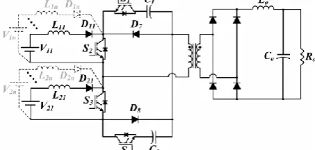
Fig. 1. Proposed multi input isolated three-level dc/dc converter.
ISSN(E): 2277-128X, ISBN: 978-93-87396-07-4, pp. 1-16
structure. The control of PCCs is integrated to the operation of the three-level bridge converter. Thus, the control complexity of the proposed converter is similar to that of a three-level dc/dc converter [24]. On the other hand, the proposed converter provides reduced part-count and lower voltage stress across the upper and lower switches. The input inductors are operated in discontinuous conducting mode (DCM), which allows autonomous power sharing between input sources with proper selection of input inductors.
This manuscript is organized as follows: Section II introduces the new multi input three-level integrated dc/dc converter and explains the operation modes in detail. In Section III, the dynamics of converter is extracted, design procedure is explained and a design example for variable input sources is given. The simulation and experimental results for a low-voltage prototype are presented in Section IV. Finally, the study is summarized and conclusion is derived in Section V.
II. PROPOSED MULTI INPUT ISOLATED THREE-LEVEL DC/DC CONVERTER
A. Topology Description
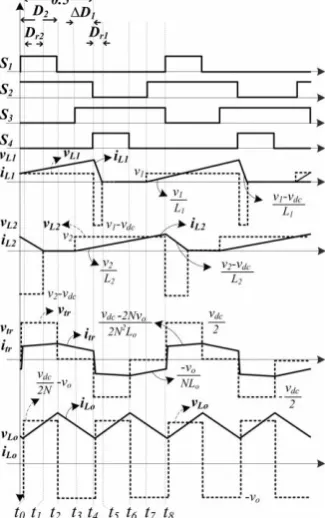
The proposed multi input converter is essentially based on the operation of the three-level isolated dc/dc converter. The secondary side rectifier can be either a half-bridge rectifier accompanied by a tapped winding for low output voltage application, or a full-bridge rectifier for high output voltage applications as shown in Fig. 1. Since the PWM scheme here is similar to that in three-level converters, the control complexity is not intensive. The boost inductors, connected to the input sources of different voltages, are charged when S2 and S3 are turned on, respectively. When the related switch (S2 or S3 ) is turned off, the energy stored in the inductor is transferred to the load. The excess or insufficient energy is either absorbed or compensated by the dc link capacitors. At the same time, S1 to S4 are switched to apply Vdc/2, –Vdc/2, and zero voltage across the primary side of the transformer. In comparison with the two-stage counterpart, two active switches and boost diodes are eliminated, while two blocking diodes are added to block the reverse current from the dc link capacitors. The switches S2 –S3 and S1 –S4 have 180° phase shift with respectto each other. The duty cycle of the middle switches should be greater than 50% such that they allow a freewheeling path for the transformer primary side current. The switching scheme is as follows: S1 is turned on right after S3 is turned off, and similarly, S4 is turned on when S2 is turned off. A dead-time should be inserted in between the turning on instant of S1 and turning off instant of S3 , and likewise between switching of S2 and S4 to avoid short circuit. The sw itching scheme of the converter is given in Fig. 2.
B. Operation Principle
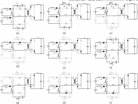
The operation modes of the circuits, which are given in Fig. 3, are explained in this section. It should be noted that these operation modes are valid when iL2 > iL1 . For this case, iL2,pk is higher than primary side of the transformer at steady state. Under this condition, iL1,pk is smaller than primary side of the transformer at steady state. If iL1 > iL2, the equivalent circuits would be different from the one presented here. Basically, the charging/discharging current of C1 and C2 would be exchanged.
ISSN(E): 2277-128X, ISBN: 978-93-87396-07-4, pp. 1-16
Fig. 3. Operation intervals of the converter. (a) Interval 1:t < t0. (b) Interval 2: t0< t < t1. (c) Interval 3: t1< t <t2(d)
Interval 4: t2< t <t3. (e) Interval 5: t3< t <t4. (f) Interval 6: t4< t <t5. (g) Interval 7: t5< t <t6. (h) Interval 8: t6< t <t7. (i)
Interval 9: t7< t <t8.
Interval 1 [t < t0]: Before t0 ,S3 is off and S1 is on. The energy stored in L2 is released to the load through the
primary winding of the transformer. The excess energy is transferred to C1 through conducting the body diode of S1 . Thus, S1 can be turned on under zero voltage with proper time delay. The current of L1 increases linearly under V1 . Total current of L2 charges C2 . Meanwhile, −Vdc/2 is applied to the primary side of the transformer
d
𝑖𝐿1(𝑡)
𝑖𝐿2(𝑡) 𝑣𝐶1(𝑡) 𝑣𝐶2(𝑡)
𝑖𝐿0(𝑡) 𝑣𝐶0(𝑡)
/dt =
𝑉1/𝐿1
(𝑉2− 𝑣𝐶1 𝑡 − 𝑣𝐶2 𝑡 )/𝐿2 𝑖𝐿2 𝑡
𝐶1 − 𝑁𝑖𝐿0(𝑡)/𝐶1
𝑖𝐿2(𝑡)/𝐶2 𝑣𝐶1 𝑡
𝑁𝐿0 − 𝑣𝐶0(𝑡)/𝐿0
𝑖𝐿0(𝑡)/𝐶0− 𝑣𝐶0(𝑡)/𝐶0𝑅0
…….(1)
Interval 2 [t0< t < t1]: At t = t0 , the current ofL1 becomes equal to that of primary side of the transformer. From
this moment on, C1 discharges over the primary side of the transformer to the load. The current of C2 is equal to that of L2 . The state equations are same as in (1).
d
𝑖𝐿1(𝑡) 𝑖𝐿2(𝑡) 𝑣𝐶1(𝑡)
𝑣𝐶2(𝑡)
𝑖𝐿0(𝑡) 𝑣𝐶0(𝑡)
/dt =
𝑉1/𝐿1
(𝑉2− 𝑣𝐶1 𝑡 − 𝑣𝐶2 𝑡 )/𝐿2 𝑖𝐿2 𝑡
𝐶1 − 𝑁𝑖𝐿0(𝑡)/𝐶1
𝑖𝐿2(𝑡)/𝐶2 𝑣𝐶1 𝑡
𝑁𝐿0 − 𝑣𝐶0(𝑡)/𝐿0
𝑖𝐿0(𝑡)/𝐶0− 𝑣𝐶0(𝑡)/𝐶0𝑅0
.….(2)
Interval 3 [t1< t < t2]: At t = t1 , the currents of L2 and C2 reach to zero. The load current is solely supplied by
ISSN(E): 2277-128X, ISBN: 978-93-87396-07-4, pp. 1-16
d
𝑖𝐿1(𝑡)
𝑖𝐿2(𝑡) 𝑣𝐶1(𝑡) 𝑣𝐶2(𝑡)
𝑖𝐿0(𝑡) 𝑣𝐶0(𝑡)
/dt =
𝑉1/𝐿1 0 −𝑁𝑖𝐿0(𝑡)/𝐶1
0
𝑣𝐶1 𝑡
𝑁𝐿0 − 𝑣𝐶0(𝑡)/𝐿0
𝑖𝐿0(𝑡)/𝐶0− 𝑣𝐶0(𝑡)/𝐶0𝑅0
.….(3)
Interval 4 [t2< t < t3]: In the beginning of this interval, S1 is turned off. The current in the leakageinductance
conducts D7 and the primary side current freewheels, hence, zero voltage isapplied across the primary side of the transformer. The output inductor voltage is equal to −Vo and the output inductor current decreases linearly
d
𝑖𝐿1(𝑡)
𝑖𝐿2(𝑡)
𝑣𝐶1(𝑡) 𝑣𝐶2(𝑡) 𝑖𝐿0(𝑡)
𝑣𝐶0(𝑡)
/dt =
𝑉1/𝐿1 0 0 0 −𝑣𝐶0(𝑡)/𝐿0
𝑖𝐿0(𝑡)/𝐶0− 𝑣𝐶0(𝑡)/𝐶0𝑅0
.….(4)
Interval 5 [t3< t < t4]: At t = t3 ,S3 is turned on, while S2 is kept on. The primary side current continues to
freewheel and zero voltage is applied across the primary side; hence, the output inductor current continuous to decrease under output voltage. Meantime, V2 is applied acrossL2 , and current increases linearly storing energy in L2
d
𝑖𝐿1(𝑡)
𝑖𝐿2(𝑡) 𝑣𝐶1(𝑡) 𝑣𝐶2(𝑡)
𝑖𝐿0(𝑡) 𝑣𝐶0(𝑡)
/dt =
𝑉1/𝐿1 𝑉2/𝐿2
0 0 −𝑣𝐶0(𝑡)/𝐿0
𝑖𝐿0(𝑡)/𝐶0− 𝑣𝐶0(𝑡)/𝐶0𝑅0
.….(5)
Interval 6 [t4< t < t5]: At t = t4 ,S2 is turned off. The stored energy in L1 is released to the load as well as to C1 .
As stated before, peak current of L1 is smaller than the load current for this case. Thus, C2 discharges over to the load and Vdc/2 is applied across the primary side of the transformer. The current of L2 continues to store energy under the influence of V2
d
𝑖𝐿1(𝑡) 𝑖𝐿2(𝑡)
𝑣𝐶1(𝑡) 𝑣𝐶2(𝑡) 𝑖𝐿0(𝑡)
𝑣𝐶0(𝑡)
/dt =
(𝑉1− 𝑣𝐶1 𝑡 − 𝑣𝐶2 𝑡 )/𝐿1 𝑉2/𝐿2
𝑖𝐿1(𝑡)/𝐶1
𝑖𝐿2 𝑡
𝐶2 − 𝑁𝑖𝐿0(𝑡)/𝐶2 𝑣𝐶2 𝑡
𝑁𝐿0 − 𝑣𝐶0(𝑡)/𝐿0
𝑖𝐿0(𝑡)/𝐶0− 𝑣𝐶0(𝑡)/𝐶0𝑅0
.….(6)
Interval 7 [t5< t < t6]: At t = t5 , the energy stored in L1 is completely transferred out. Its current reaches to zero
at DCM. The load current is solely supplied by C2
d
𝑖𝐿1(𝑡)
𝑖𝐿2(𝑡)
𝑣𝐶1(𝑡) 𝑣𝐶2(𝑡) 𝑖𝐿0(𝑡)
𝑣𝐶0(𝑡)
/dt =
0 𝑉2/𝐿2
0 −𝑁𝑖𝐿0(𝑡)/𝐶2
𝑣𝐶2 𝑡
𝑁𝐿0 − 𝑣𝐶0(𝑡)/𝐿0
𝑖𝐿0(𝑡)/𝐶0− 𝑣𝐶0(𝑡)/𝐶0𝑅0
.….(7)
Interval 8 [t6< t < t7]: In this interval, S4 is turned off. The current in the leakage inductance conducts D8 and
the primary side current freewheels, hence, zero voltage is applied across the primary side of the transformer. The current of L2 continues to increase
d
𝑖𝐿1(𝑡) 𝑖𝐿2(𝑡)
𝑣𝐶1(𝑡)
𝑣𝐶2(𝑡) 𝑖𝐿0(𝑡)
𝑣𝐶0(𝑡)
/dt =
0 𝑉2/𝐿2
0 0 −𝑣𝐶0(𝑡)/𝐿0
𝑖𝐿0(𝑡)/𝐶0− 𝑣𝐶0(𝑡)/𝐶0𝑅0
.….(8)
Interval 9 [t7< t < t8]: At t = t7 ,S2 is turned on while S3 remains at on-state. The primary side current continues
ISSN(E): 2277-128X, ISBN: 978-93-87396-07-4, pp. 1-16
d
𝑖𝐿1(𝑡) 𝑖𝐿2(𝑡)
𝑣𝐶1(𝑡)
𝑣𝐶2(𝑡) 𝑖𝐿0(𝑡)
𝑣𝐶0(𝑡)
/dt =
𝑉1/𝐿1
𝑉2/𝐿2 0 0 −𝑣𝐶0(𝑡)/𝐿0 𝑖𝐿0(𝑡)/𝐶0− 𝑣𝐶0(𝑡)/𝐶0𝑅0
.….(9)
III. ANALYSIS OF THE PROPOSED CONVERTER
A. Averaged State-Variables
In order to obtain the averaged values for state variables, the expressions for state variables given in (1) to (9) are averaged over the given time intervals. The input inductor current can be averaged over the switching period as
d𝑖𝐿1/dt =𝐿𝑉1 1d1 +
𝑉1−𝑣𝐶1−𝑣𝐶2
𝐿1 dr1 .….(10)
where dr1 denotes the duty ratio of the time interval in which inductor current decreases from its peak value to zero, when
the boost switch is turned off. dr1 is a function of state variables; however it is yet neither a state nor a control variable.
To substitute d with state variables, one can use voltage-balance law of inductor. When the boost switch is turned on, the peak inductor current becomes
iL1.pk =
𝑉1
𝐿1 d1Ts .….(11)
When the boost switch is turned off, it becomes
iL1.pk =
𝑉1−𝑣𝐶1−𝑣𝐶2
𝐿1 dr1 Ts .….(12)
Equalizing (11) and (12), and solving it for dr1 yields
dr1 =
𝑉1
𝑉1−𝑣𝐶1−𝑣𝐶2d1 .….(13)
This conversion expresses dr1 in terms of control variable, d1 and state variables vc1 and vc2. Substituting (13)
into (9) results in diL1 /dt = 0; thus losing the dynamic inductor current information, which can be referred as reduced
order modeling. In order to obtain a full order model, the average inductor current expression can be used for finding out dr1
𝑖𝐿1=iL1.pk
2 (d1 + dr1) …….(14)
By substituting (12) into (14), an expression which relatesdr1 with d1 and 𝑖𝐿1 can be derived
dr1=
2𝑖𝐿1𝐿1
𝑉1 d1 Ts ……..(15)
The averaged inductor currents over the switching period can be found by inserting (15) into (10) as
d𝑖𝐿1/dt =𝑣𝐶1+𝑣𝐶2
𝐿1 d1 +
2𝑖𝐿1 d1Ts
𝑉1−𝑣𝐶1−𝑣𝐶2
𝑉1 ……..(16)
d𝑖𝐿2/dt = 𝑣𝐶1+𝑣𝐶2
𝐿2 d1 +
2𝑖𝐿2 d1Ts
𝑉2−𝑣𝐶1−𝑣𝐶2
𝑉2 ……..(17)
By using the same conversion and principle, the averaged expressions for the state variables of dc link capacitor voltages, output inductor and voltage can be found analogously. These state-equations are of paramount significance in analyzing the dynamic behavior of the converter as well as in designing the controller
d𝑣𝐶1/dt = 𝑖𝐿1𝐶 +𝑖𝐿2
1 -
𝑑12Ts 2𝐶1
𝑉2
𝐿2+
𝑉1 𝐿1 − 𝑑2
𝑁 𝑖𝐿𝑂
𝐶1 ……..(18)
d𝑣𝐶2/dt = 𝑖𝐿1 +𝑖𝐿2
𝐶2 -
𝑑12Ts 2𝐶2
𝑉2
𝐿2+
𝑉1 𝐿1 − 𝑑2
𝑁 𝑖𝐿𝑂
𝐶2 ……..(19)
d𝑖𝐿0/dt = 𝑣𝐶1𝑁𝐿+𝑣𝐶2
0 d2 - 𝑣𝐶0
𝐿𝑂 ……..(20)
d𝑣𝐶𝑜/dt = 𝑖𝐶𝐿𝑜
𝑂 - 𝑣𝐶0
𝐶0 𝑅𝑂 ……..(21)
B. Design Considerations
As denoted in Section II, the minimum duty ratio of the middle two switches, D1 , should be at least 50%, in
order to apply zero voltage to the primary side of the transformer. The remaining 50% is shared between the duty ratios of S1 and S4 , denoted by D2 , and control signal of S2 and S3 , denoted by ΔD1 . This leaves a margin for the control of
ISSN(E): 2277-128X, ISBN: 978-93-87396-07-4, pp. 1-16
D1 = 0.5+ΔD1……….(22)
Where
ΔD1 = 0.5 − D2,max . ……….(23)
1) Determination of Lo ,D2 , ΔD1 : The load side of the converter can be designed to operate in either CCM or DCM
mode. The output inductor current can be continuous or discontinuous depending on the design criteria, or else it might be designed such that the operation of the converter can transit to DCM at light load condition to reduce the size of the output inductor. The required output inductance value can be determined by (24)
𝐿𝑂≥ 𝑉02 (0.5−𝐷𝑚𝑖𝑛)
2 𝑃𝑥𝑓𝑠 ……….(24)
where Px represents the minimum output power at which the converter is desired to be operated in CCM. When output inductor operates in CCM mode, D2 can be expressed as in (25) at steady state
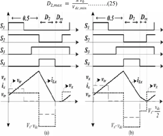
𝐷2,𝑚𝑎𝑥 = 𝑁 𝑉0
𝑉𝑑𝑐 ,𝑚𝑖𝑛……….(25)
Fig. 4. DCM/CCM boundary cases. (a) Input inductor current reaches to zero within D2 Ts . (b) Input inductor current
reaches to zero within (D2 + Drx )Ts
where N represents the turns ratio of the transformer windings. The equivalent duty ratio for DCM mode can be written as
𝐷2= 2 𝐿𝑂 𝑅Ts( 𝑉 𝑑𝑐
𝑁 𝑉 0−1 2−1)
……….(26)
Depending on the operation mode, N can be found from either (25) or (26). Once D2,max and Vdc,min are
determined, D1 and the limits for ΔD1 can be found using (22)and (23).
2) Determination of DCM Boundary and DC Link Voltage: In this paper, the operation principle is based on operating input inductors in DCM. This is due to the fact that input sources are controlled by D1 and their voltages can be different,
only one of the cells would be able to operate in CCM, while the other one would continue operating in DCM. Once one of the input sources transits to CCM, the continuous current forces to apply −Vdc to the other input, which keeps the
voltage of latter at the same level; hence, latter continues to provide same amount of power in DCM mode. The rest of the necessary power is supplied from the input source operating in CCM. This operation could be considered for applications where output power of one of the input sources is maximized to definite value, while the secondary input source provides rest of the load power demand. The operation modes shown in Fig. 3 has been given considering that the input inductors are well chosen for DCM operation under any load, and input inductor currents reach to zero within D2Ts
In case this interval lasts longer depending on the chosen parameters and output power, there could be one more operation mode, which was not shown in Fig. 3. It is yet necessary to analyze this operation mode in order to define the CCM/DCM boundary. In such a circumstance, after the operation interval 7, the upper inductor would still continue to provide energy to the upper capacitor even after S4 is turned off under the influence of Vdc/2. The voltage of the primary
side of the transformer remains at zero since D8 conducts. Relevant waveforms are illustrated in Fig. 4.
ISSN(E): 2277-128X, ISBN: 978-93-87396-07-4, pp. 1-16
𝐷1= 𝑉𝑑𝑐 ,𝑐𝑟𝑡− 𝑉𝑥 𝐷2+ (
𝑉𝑑𝑐 ,𝑐𝑟𝑡
2 − 𝑉𝑥 ) (1−𝐷1− 𝐷2) ……….(27)
where Vx denote the voltage of the input source that provides higher output power. The lowest dc link voltage that should
be adopted for DCM operation can be expressed as
𝑉𝑑𝑐 ,𝑐𝑟𝑡 = 2 𝑉𝑥
𝐷2−𝐷1 +1……….(28)
For DCM operation, the following condition should be satis- fied: 𝑉𝑑𝑐 ,𝑚𝑖𝑛>𝑉𝑑𝑐 ,𝑐𝑟𝑡.
3) Determination of L1 and L2 : In this paper, the operation principle is based on operating input inductors in DCM. For
the proposed converter, the duty ratios of S2 and S3 are the same, and equal to D1 . Hence, the output power of each cell is
proportional to the square of its input voltage, and inversely proportional to the inductance. The total power fed by the input sources can be expressed as
𝑃0= η𝑉𝑑𝑐 𝐷12Ts 2
𝑉𝑛2 𝐿𝑛(𝑉𝑑𝑐− 𝑉𝑛) 𝑛
1 ……….(29)
Thus, with proper design of these parameters with respect to behaviors of input source, an autonomous power sharing is possible. Based on (29) there are various possibilities to determine L. The bottom boundaries for Ln based on
𝑉𝑛 ,𝑚𝑖𝑛 and output power are defined as
𝑃𝑚𝑎𝑥 = η
𝑉𝑑𝑐𝐷1,𝑚𝑎𝑥2 Ts 2
𝑉𝑛 ,𝑚𝑖𝑛2
𝐿𝑛(𝑉𝑑𝑐− 𝑉𝑛 ,𝑚𝑖𝑛) 𝑛
1 ……….(30)
The values of the inductances can be determined for rated power, which would fall into the boundary defined above.
Fig. 5. Inductance determination based on power sharing when V1 = V1,min , V2 = V2,min .
The determination of inductances depends on the application needs. For instance, for PV generation systems, the inductances can be calculated according to the desired load sharing at the maximum power operation point.
C. Design Example
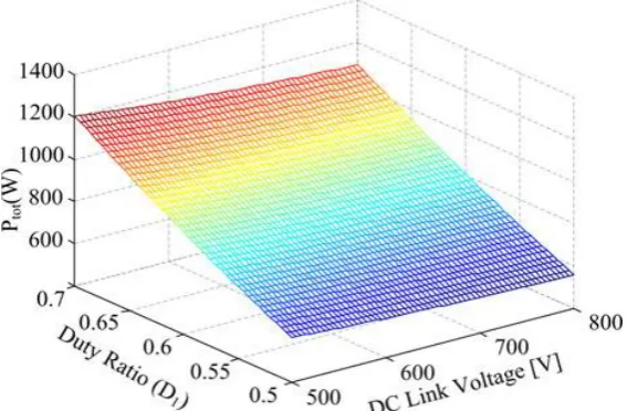
The design procedure for constant power loads with constant input voltage sources is straightforward. Thus, this section illustrates a design procedure for an application with dynamic variables having the parameters of V1,min = 110 V,V1,max = 130 V,V2,min = 100 V,V2,max = 150 V,Vo = 200 V,Ptot,max = 1.2kW,fs = 50 kHz. In typical bridge-type isolated converters, the duty ratio of the second stage, D2 , is between 0.48 and 0.25. Since there is a limitation on the duty cycles in the proposed converter, as stated in (21) and (22), D1,max can be set to 0.7, where ΔD1 becomes 0.2. In this case, D2,max is equal to 0.3. Using (27), the critical dc link voltage, Vdc,crt, is calculated as 500 V; thus, Vdc,min is determined as 500 V. From (24), transformer turns ratio is calculated as 0.75.
Based on the condition given in (29), all possible L1 and L2 combinations can be found. Another criterion in determining the inductances is the power ratio among the input sources at desired input voltages. For this design, the power ratio of the second input source to the first input source at maximum output power and minimum input voltages, denoted as αP , is evaluated. Based on the chosen αP , the values of the inductances can be determined as shown in Fig. 5. In this study, αP is determined as 0.7, which means that the second source provides 500 W and the first source provides 700 W under maximum load when V1 = V1,min , and V2 = V2,min . The corresponding L1 and L2 values, are selected from Fig. 5; L1 = 108 μH,L2 = 122 μH.
ISSN(E): 2277-128X, ISBN: 978-93-87396-07-4, pp. 1-16
Fig. 6. Power can be drawn from the first input source at Vdc = 500 V under DCM mode.
Fig. 7. Power can be drawn from the second input source at Vdc = 500 V under DCM mode.
Fig. 8. Power can be drawn from both input sources at various dc link voltages when V1 = V1,min , V2 = V2,min .
ISSN(E): 2277-128X, ISBN: 978-93-87396-07-4, pp. 1-16
Fig. 9. Simulation waveforms when V1 = V2 = 150 V, L1 = 200 μH, L2 = 100 μH. (a) Transformer’s primary winding voltage, and input inductor voltages. (b) Input boost inductor currents. (c) Transformer’s primary winding current and
output inductor current. (d) Dc bus capacitor voltage ripples. (e) Dc bus capacitor currents.
ISSN(E): 2277-128X, ISBN: 978-93-87396-07-4, pp. 1-16
Fig. 10. Simulation waveforms when V1 = 150 V, V2 = 50 V, L1 = L2 = 100 μH. (a) Transformer’s primary winding voltage, and input inductor voltages. (b) Input boost inductor currents. (c) Dc bus capacitor voltage ripples. (d) Dc bus
capacitor currents.
III. SIMULATION AND EXPERIMENTAL RESULTS
ISSN(E): 2277-128X, ISBN: 978-93-87396-07-4, pp. 1-16
Fig. 11. Photo of the designed prototype
In Fig. 9(a), it can be observed that even though same voltage is applied to the inductors, the output power contribution is different due to the chosen different inductances. For this case, the output power is 1.6 kW and iL2,pk > iL1,pk . The charging/discharging current of C2 is higher than that of C1 , resulting in asymmetrical voltage ripples across two dc bus capacitors.
The corresponding results for latter simulation are given in Fig. 10. As it can be seen from Fig. 10(a), the applied voltages are different while the chosen inductances are same. For this case, iL1,pk > iL2,pk and the capacitor charging currents and thereby the capacitor voltage ripples are replaced. It is worth mentioning that the feedback voltage signal should be averaged over the switching period for capacitor voltage balancing.
Due to the asymmetry of the voltage source, the capacitor currents are different, resulting in different capacitor voltage ripples. Like in any other multilevel converter, the capacitor voltages should be balanced. For the proposed converter, this can be achieved by adding a compensating signal to the duty ratio of S1 and S4 , which either extends or shortens its effective duty ratio.
A low voltage laboratory built prototype has been designed and tested, as shown in Fig. 11, to serve as a proof-of-concept. The input inductances (L1 = L2 ) are 87 μH each, dc link capacitances (C1 = C2 ) are 470 μF each. The output capacitor (Co ) is 220 μF and output inductor (Lo ) is 200 μH. The secondary side of the transformer has a tapped winding configuration followed by a half-bridge rectifier. The transformer has 1:1 turns ratio for each secondary winding. The ratings of the switches are 600 V/22 A. The switching frequency is 50 kHz. The pulse pattern is generated using Texas Instrument’s floating point DSP.
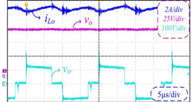
The tests are conducted for two different duty cycles. The experimental results are verified with simulation results under the same operation conditions. Fig. 12 portrays the switching pattern when D1 = 0.6 and D2 = 0.35. It should be noted that the inverse of the gating signals are shown here due to the hardware configuration. The experimental and simulation results for V1 = 70 V and V2 = 90 V are shown in Figs. 13 and 14, respectively
ISSN(E): 2277-128X, ISBN: 978-93-87396-07-4, pp. 1-16
Fig. 13. Experimental results of dc link voltage, transformer voltage, input inductor currents when D1 = 0.6, D2 = 0.35, V1 = 70 V and V2 = 90 V.
Fig. 14. Simulation results of dc link voltage, transformer voltage, input inductor currents when D1 = 0.6, D2 = 0.35, V1 = 70 V and V2 = 90 V.
The peak current of the first inductor is 9.5 A, whereas the peak of the second inductor is 12.5 A. In this case, the power ratio of the second source to the first one is 1.8. The output voltage and current are around 75 V, and 9.2 A, respectively, as shown in Fig. 15. On the other hand, the output voltage is little higher in the simulation due to ideal and lossless components as well as the precise transformer ratio, as it can be seen from Fig. 16.
In the second set of experiments, D1 and D2 are adjusted to 0.7 and 0.25, respectively. The first source voltage is varied between 60–70 V, while the second source voltage is swept from 70–110 V. The gating signals of the switches are given in Fig. 17. In Figs. 18 and 19, both input source voltages are set to 70 V. As seen from the figures, both sources supply 9.5-A peak current, and share the load demand equally. In Figs. 20 and 21, the second source voltage is set to 100 V. The peak current is increased to 14.5 A. The power distribution of the second source to the first source becomes 2.15. In Figs. 22 and
ISSN(E): 2277-128X, ISBN: 978-93-87396-07-4, pp. 1-16
Fig. 16. Simulation results of output voltage, transformer voltage, output inductor current when D1 = 0.6, D2 = 0.35, V1 = 70 V and V2 = 90 V.
Fig. 17. Experimental waveforms of gate signals when D1 = 0.7, D2 = 0.25.
Fig. 18. Experimental results of dc link voltage, transformer voltage, input inductor currents when D1 = 0.7, D2 = 0.25, V1 = 70 V and V2 = 70 V.
ISSN(E): 2277-128X, ISBN: 978-93-87396-07-4, pp. 1-16
Fig. 20. Experimental results of dc link voltage, transformer voltage, input inductor currents when D1 = 0.7, D2 = 0.25, V1 = 70 V and V2 = 100 V.
Fig. 21. Simulation results of dc link voltage, transformer voltage, input inductor currents when D1 = 0.7, D2 = 0.25, V1 = 70 V and V2 = 100 V.
Fig. 22. Experimental results of dc link voltage, transformer voltage, input inductor currents when D1 = 0.7, D2 = 0.25, V1 = 60 V and V2 = 110 V.
ISSN(E): 2277-128X, ISBN: 978-93-87396-07-4, pp. 1-16
The experimental efficiency data of the converter under three different operating conditions are presented in Table I, and divided into its individual loss components. The proposed converter exhibited 87–88.6% efficiency under the given test conditions. For a fair comparison, a two-stage counterpart is built by unplugging the input sources from the power terminals, and connecting two interleaving boost legs to the dc link. Theswitching scheme and operating conditions are kept same as of the proposed converter. The two-stage counterpart exhibits higher efficiency than the proposed one, between 89.4–90.1%. Thus, the efficiency of the proposed single-stage converter is 1.5–2.4% lower than the two-stage counterpart. The slightly reduced efficiency is the main disadvantage in single-stage converters in general, opposed to the low cost feature, including the eliminated switches, and corresponding gate driver circuits. In Table I, PBD Sn ,PD Boostn ,PCon BtSn and PD Blockn denote the losses of the body diodes of the switches, boost diodes and boost switches present in two-stage converter, and blocking diodes in series with the inductors in the proposed converter, respectively. The other losses such as core losses and parasitic capacitance losses are summed and given under Pun−meas. As it can be seen from Table I, although additional switches introduce extra losses in the two-stage counterpart, conduction and switching losses of the middle two switches in the proposed converter surpass the other losses, and reduces the converter’s overall efficiency. This is due to the single-stage operation as both the rms and the peak currents of the middle two switches increase significantly. In addition, the transition voltages across the middle two switches are equal to bus voltage, which increases the turn-off switching losses. On the other hand, the currents passing through the upper and lower switches reduce due to single-stage operation. Nevertheless, this reduction does not compensate the additional losses caused by the middle two switches.
IV. CONCLUSION
In this study, a new multi input dc/dc converter having same number of active switches as of three-level isolated dc/dc converter without introducing additional switching actions is proposed. The circuit analysis and design consideration has been provided in detail. With proper selection of input inductors, autonomous load sharing can be achieved. To verify the operation of the converter, simulations of different parameters have been performed. A low voltage laboratory built prototype has been designed and tested under varying input voltages and duty cycles. The results prove the effective integrated operation of input sources with three-level isolated dc/dc structure, through operating four switches in a phase-shifted manner without introducing control complexity.
REFERENCES
[1] A. Khaligh, A. M. Rahimi, Y.-J. Lee, J. Cao, A. Emadi, S. D. Andrews, C. Robinson, and C. Finnerty, “Digital control of an isolated active hybrid fuel cell/li-ion battery power supply,” IEEE Trans. Veh. Technol., vol. 56, no. 6, pp. 3709–3721, Nov. 2007.
[2] K. Kobayashi, H. Matsuo, and Y. Sekine, “Novel solar-cell power supply system using a multiple- input DC– DC converter,” IEEE Trans. Ind. Electron., vol. 50, no. 1, pp. 281–286, Feb. 2006.
[3] O. C. Onar and A. Khaligh, “A novel integrated magnetic structure based DC/DC converter for hybrid battery/ultracapacitor energy storage systems,” IEEE Trans. Smart Grid, vol. 3, no. 1, pp. 296–307, Mar. 2012.
[4] M. Marchesoni and C. Vacca, “New DC–DC converter for energy storage system interfacing in fuel cell hybrid electric vehicles,” IEEE Trans. Power Electron., vol. 22, no. 1, pp. 301–286, Jan. 2007.
[5] F. Liu, Z. Wang, Y. Mao, and X. Ruan, “Asymmetrical half-bridge double-input DC/DC converters adopting pulsating voltage source cells for low power applications,” IEEE Trans. Power Electron., vol. 29, no. 9, pp. 4741–4751, Sep. 2014.
[6] M. Marchesoni and C. Vacca, “New DC–DC converter for energy storage system interfacing in fuel cell hybrid electric vehicles,” IEEE Trans. Power Electron., vol. 22, no. 1, pp. 301–286, Jan. 2007.
[7] F. Liu, Z. Wang, Y. Mao, and X. Ruan, “Asymmetrical half-bridge double-input DC/DC converters adopting pulsating voltage source cells for low power applications,” IEEE Trans. Power Electron., vol. 29, no. 9, pp. 4741–4751, Sep. 2014.
[8] A. D. Napoli, F. Crescimbini, and S. Rodo, “Multiple input dc/dc converter for fuel-cell powered hybrid vehicles,” in Proc. IEEE Power Electron. Spec. Conf., 2002, pp. 1685–1690.
[9] H. J. Chiu, H. M. Huang, L. W. Lin, and M. H. Tseng, “A multiple-input dc/dc converter for renewable energy system,” in Proc. IEEE Int. Conf. Ind. Technol., 2005, pp. 1304–1308.
[10] Y. M. Chen, Y. C. Liu, and T. F. Wu, “Multi- input dc–dc converter based on the multiwinding transformer for renewable energy applications,” IEEE Trans. Ind. Appl., vol. 38, no. 4, pp. 1096– 1104, Jul./Aug. 2002. [11] J. L. Duarte, M. Hendrix, and M. G. Simoes, “Three-port bidirectional converter for hybrid fuel cell
ISSN(E): 2277-128X, ISBN: 978-93-87396-07-4, pp. 1-16
[12] S. Danyali, S. H. Hosseini, and G. B. Gharehpetian, “New extendable single stage multi-input DC–DC/AC boost converter,” IEEE Trans. Power Electron., vol. 29, no. 2, pp. 775– 788, Feb. 2014.
[13] B. G. Dobbs and P. L. Chapman, “A multiple- input DC-DC converter topology,” IEEE Power Electron. Lett., vol. 1, no. 1, pp. 6–9, Mar. 2003.
[14] A. Khaligh, J. Cao, and Y.-J. Lee, “A multiple- input DC–DC converter topology,” IEEE Trans. Power Electron., vol. 24, no. 3, pp. 862–868, Mar. 2009.
[15] R.-J. Wai, C.-Y. Lin, J.-J. Liaw, and Y.-R. Chang, “Newly designed ZVS multi-input converter,” IEEE Trans. Ind. Electron., vol. 58, no. 2, pp. 555–566, Feb. 2011.
[16] A. Kwasinski, “Identification of feasible topologies for multiple-input DC–DC converters,” IEEE Trans. Power Electron., vol. 24, no. 3, pp. 856–861, Mar. 2009.
[17] Y. Yuan-mao and K. W. E. Cheng, “Multi-input voltage-summation converter based on switched- capacitor,” IET Power Electron., vol. 6, no. 9, pp. 1909–1916, Nov. 2013.
[18] H. Wu, J. Zhang, and Y. Xing, “A family of multi-port buck-boost converters based on DC- link-inductors (DLIs),” IEEE Trans. Power Electron., vol. 30, no. 2, pp. 735–746, Feb. 2015.
BIOGRAPHY
Chintala Venkatesh received his B.Tech. Degree in Electrical and Electronics Engineering from JNTU University, Anantapur, Andhra Pradesh, India. He obtained M.Tech in Power Electronics from JNTU University, Anantapur, Andhra Pradesh, India. Presently he is pursing Ph.D under Anna Universit, Chennai, Tamilnadu, India. Presently he is working as an Assistant Professor in the SMK FOMRA Institute of Technology, Chennai, Tamilnadu, India.