Ensuring a High Quality Digital Device
through Design for Testability
Christopher Umerah Ngene
Department of Computer Engineering, University of Maiduguri, Nigeria
An electronic device is reliable if it is available for use most of the times throughout its life. The reliability can be affected by mishandling and use under abnormal operating conditions. High quality product cannot be achieved without proper verification and testing during the product development cycle. If the design is difficult to test, then it is very likely that most of the faults will not be detected before it is shipped to the customer. This paper describes how product quality can be improved by making the hardware design testable. Various designs for testability techniques were discussed. A three bit counter circuit was used to illustrate the benefits of design for testability by using scan chain methodology.
Keywords: design for testability, digital devices, faults, defect level, reliability, testing
1. Introduction
A look at the electronic market will reveal that a lot of substandard electronic goods abound in the market such that consumers find it difficult to differentiate between the brand names and fakes. No thanks to unethical practices of some organisations that are deeply involved in cloning and reverse engineering of the branded goods. The reliability of electronic system used to be the concern of the military, aerospace and bank-ing industries. But today applications such as computers, consumer electronics, telecommu-nication and automotive industries have joined the league of applications that demands relia-bility and testing techniques because they are everywhere and their feature sizes have become less and less as the years go by. In addition, their proliferation has led to the tendency of their misuse. An important aspect of reliability is the system’s ability to run independently on demand. This requires that the system be fault tolerant.
Poor quality products require more maintenance and repairs which leads to huge expenses on staff and mileage to get staff and spares to out-door locations[4]. It also affects the manufac-turer’s image and costs on returned parts and systems.
The three basic engineering activities are de-sign, manufacture and test. Currently testing activities are also carried out at the design stage. This means that testing process is integral to both design and manufacturing actions and can-not be seen as a standalone activity. These ac-tivities are done as quickly as possible and eco-nomically too. Because we want to save time and cost, we should endeavour to ensure that the quality of the would-be product is not compro-mised. Even while a product is in use testing can also be carried out, either as a normal rou-tine service arrangement or to eliminate faults as they occur.
not be able to say what happens after packaging and when the component is finally mounted on a board and delivered to the consumer. It is im-portant to note that ICs at the end of the day find their ways onto a circuit board. Even Systems on chip(SoC)end up on a board. While on the board, we have to boarder about how well the pins of the various ICs mounted on the board are connected or whether the right IC is in the right position.
Testing encompasses design verification and di-agnosis(fault location for purposes of effecting repairs). There are two aspects to test. One is testing the design, or carrying out design veri-fication to make sure that the design is correct and conforms to requirements. Design verifi-cation also lets you know where you are in the development cycle and how stable the design is [1]. The other aspect of test is testing for physical failures, making sure nothing has been broken and there’s no defect from manufactur-ing. A significant portion of our development cycle time is spent on testing the product design, and that’s becoming extremely expensive. The beauty of integrated design and manufac-turing is that it cuts product cycle time, but successful integration hinges on the quality of the design data passed to manufacturing. The remaining parts of this paper are divided into sections. In Section 2, the challenges of prod-uct quality will be discussed. Section 3 briefly discusses the design flows with integrated test-ing. In Section 4, this paper reviews faults and test pattern generation, whereas Section 5 x-rays ways of making designs testable. A simple example to illustrate the design for testability technique using scan chain methodology is pre-sented in Section 6.
2. Electronic Product Quality Challenges
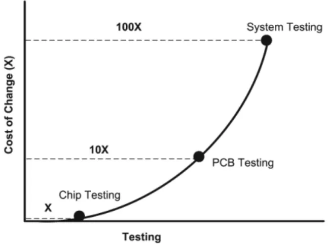
Quality improvement starts at the design stages. It is a standard in electronics industry to test chips before they are mounted on a board, test the board before system assembly and finally test the system. This is essentially so because of the rule of ten. If a chip fault is not caught by chip testing, finding the fault costs 10 times as much at the PCB level as at the chip level. Similarly, if a board fault is not caught by PCB testing, finding the fault costs 10 times as much
at the system level as at the board level. This means that a fault that is not caught at the chip level will now cost 100 times as much as at the system level.
Some engineers are suggesting that rule of twenty be adopted considering the complex nature of present day ICs. The rule of ten is illustrated in Figure 1. Very real costs are associated with inattention to design quality. If errors or omis-sions in design data are not addressed early, more costly changes are required later in the product development process.
Figure 1.Rule of ten.
Another development is the synthesis for dif-ferent objectives. Early synthesis was aimed at decreasing area and delay. More recently, other objectives have come into play, such as power, noise, thermal control, verifiability, manufac-turability, variability, and reliability. Conse-quently, additional criteria will emerge as new technologies develop, and new models and op-timization techniques will be needed to address such requirements[12].
2.1. Concept of Reliability
Reliability is the probability of no failure within a given operating period. For example, if 50 systems operate for 1,000 hours on test and two fail, then using expression(1)we would say that the probability of failure,Pf, for this system in
1,000 hours of operation is 0.04. Clearly, the probability of success,Ps, which is known as the
is equal to 0.96 using expression(2).
pf = Number failed systems
total number systems (1)
ps = 1− pf (2)
One can also deal with a failure rate,fr, for the
same system. Substituting the values in expres-sion (3), failure rate equals 4×10⁻⁵ or, as it
is sometimes stated, fr = z = 40 failures per
million operating hours, wherezis often called the hazard function.
fr = Number failed systems
total number systems × hours (3)
If failure ratezis a constant(one generally uses λ to represent a constant failure rate), the re-liability function can be shown to be equation (4).
R(t) =e−λt (4)
The mean time between failures(MTBF):
MBTF=
∞
0
e−λtdt= 1
λ (5)
The repair time(Rep)is also assumed to obey an exponential distribution and is given by ex-pression(6).
Rep(P>t) =e−μt. (6)
The mean time to repair(MTTR)is represented in equation(7):
MTTR = 1
μ (7)
where μ is the repair rate. The system avail-ability (failure-free) is the fraction of time the system is operating normally and is given by expression(8):
System Availability MTBF
MTBF+MTTR (8)
With the expression (4) for reliability it be-comes evident that the more complex a system is, the less its reliability. For instance, if a sys-tem board contains n number of components and each component has a reliability ofRc, the
reli-ability of the board (Rsb)over timetperiod of
operation without failure is given by expression (9):
Rsb[Rc(t)]n = [e−λt]n=e−nλt (9)
It is therefore clear that the system reliability is very small, not minding the fact that the relia-bility of individual component is high and will reduce further if the reliability of the intercon-nections are taken into consideration.
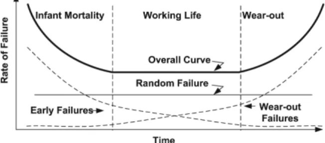
The graphical representation of failure rateZ(t)
as a function of time can be illustrated by the popular bathtub curve shown in Figure 2.
Figure 2.Failure rate curve.
The infant mortality region in the graph depicts failures that are attributed to poor quality as a result of variations in the production process technology. The region in the graph termed “Working life” shows that the failure rate is constant (Z(t) = λ). This is the working life of a component or system and fault occurrence here is random. The wear out region marks the end-of-life period of a product. For electronic products it is assumed that this period is less important because they will not enter this re-gion due to a shorter economic lifetime resulting from technology advances and obsolescence. It is important to note here that all ICs must be shipped after they have passed infant mortality test periods in order to reduce field failure and subsequent repairs.
2.2. Temperature Effect on Reliability
and therefore, rate of a chemical reaction.
λT2=λT1×e(Ea(1/T1−1/T2)/k) (10) Where:
Eais the activation energy expressed in
Electron-volts(eV)
kis the Bolzmann constant 8.617×10⁻⁵eV/K
T1 andT2 are absolute temperatures(in Kelvin, K),
λT1 andλT2 are the failure rates atT1 andT2, respectively.
From equation(10)it is evident that the failure rate is exponentially dependent on the temper-ature. The ratio of λT2 to λT1 gives us the acceleration factor effect of temperature. This is the factor by which the infant mortality can be reduced during burn-in testing.
3. Design Flows
The design of VLSI follows certain procedure, evolving from the highest level of abstraction down to implementation – Design Specifica-tion, HDL Capture, RTL Simulation & Func-tional Verification, RTL Synthesis, FuncFunc-tional Gate Simulation, Place and Route and Post Lay-out Timing Simulation.
Every design starts with specification capture. We must determine the functionality of the new design at the onset. Wrong conception at this level could lead to a lot of problems such as poor quality product. An idea of what is to be de-signed is converted into formal document called design specification. In some cases one or more specification documents are created, depend-ing on whether we are creatdepend-ing a component or a system. Design specification is a written statement of functionality, timing, area, power, testability, fault coverage, etc. The following methods are used to specify the functionality – state transition graphs, timing charts, algorith-mic state machines and hardware description languages (VHDL and Verilog). Lately, the need to capture designs at the highest level of abstraction in what is called Electronic System Level (ESL) using SystemC, System Verilog, etc. is being integrated and pursued vigorously. The specification is then captured using HDL in form of behavioural description. The HDL model of the design is simulated in order to determine functional compliance and to expose
any design or coding errors. In order to achieve this, a test plan is developed. This involves writ-ing a test bench for the model and applywrit-ing ap-propriate test vectors to verify the design. If the functionality has been verified, then the model is synthesised using appropriate synthesis tools. The objective of synthesis is to produce the netlist (list of modules and their interconnec-tion at the register transfer level stage or at the gate level)of the design for the target technol-ogy. Synthesising the design involves optimisa-tion of Boolean funcoptimisa-tions(minimise logic, re-duce area, rere-duce delay, rere-duce power, balance speed versus other resources consumed). After the RTL/gate level synthesis, the design is fur-ther simulated to determine that the gates used function properly and meet the overall function-ality. If this is achieved, then we move on to the placement and routing stage where selected cells are placed on the target technology(CPLD, FPGA or ASIC) and connected in accordance with the netlist. After the placement and rout-ing have been completed, the need to further simulate the design arises. In this case we sim-ulate to determine whether the timing (timing back-annotation), speed, physical and electrical specifications have been met. This simulation includes test vector generation to test inherent fabrication flaws. It is important to note that the design should be correct at this stage, because this is the last stage before the design is signed off for fabrication. You can see that testing is carried out virtually at all the stages of the de-sign flow. This is important because the earlier an error is detected, the better and, of course, the cheaper.
Testing, on the other hand, is a set of activi-ties designed to ensure that a circuit that has been manufactured complies with the paramet-ric (voltage, resistance, current, capacitance, etc), timing and functional specifications of the design. In other words testing demonstrates that the manufactured IC is error free. Digital test-ing is performed on the manufactured IC ustest-ing test patterns generated to demonstrate that the product is fault-free. It is important to note that, at the logic gate level, automatic test pattern generation(ATPG)is used to generate the test patterns and they are verified using fault sim-ulators. At higher levels of abstraction (RTL and behavioural)testability measures are used instead.
Rapidly evolving submicron technology and de-sign automation has enabled the dede-sign of elec-tronic systems with millions of gates integrated on a single silicon die, capable of delivering gi-gaflops of computational power. At the same time, increasing complexity and time to market pressures are forcing designers to adopt design methodologies with shorter ASIC design cycles. With the emergence of system-on-chip (SoC) concept, traditional design and test methodolo-gies are hitting the wall of complexity and ca-pacity. Conventional design flows are unable to handle large designs made up of different types of blocks such as customized blocks, pre-designed cores, embedded arrays, and random logic. A key requirement for obtaining reliable electronic systems is the ability to determine that the systems are error-free [6]. Electronic systems consist of hardware and software. In this paper we shall be looking at hardware testa-bility issues. What is a system? Semiconductor components are not thought of as systems. A system is a collection of components that forms a complete item that one can procure to do a specific task or function. A system also in-cludes a hierarchy of other systems, which we call subsystems, each of which is a system in its own right. In [1] Hal Carter opined that the basic philosophy is that systems grow as large as our technology will permit and testing complexity also grows. In the words of Carter, “You have to be able to distribute the testing load down to the lower level so that you don’t impose that entire load on the highest complex-ity of the system” [1]. If you take n units and combine them such that they all interact, you’ll get n(n−1)/2 interconnections, which is an2
product of the communication complexity be-tween the units. If you can decompose that, you can get down to logncomplexity for the num-ber of units actually being diagnosed or tested. Design-for-test and self-test must therefore be involved with components at as many levels as possible. Then system-level testing can actu-ally aggregate those lower level tests in a more streamlined way as they migrate towards the system as a whole[1].
4. Review of Faults and Test Pattern Generation
With the present deep sub-micron technology which is currently at 20 nm [7] ensuring high product reliability has become more daunting. The more transistors/gates we squeeze into a small area of a chip the greater the risk of over heating, crosstalk between interconnections and the more likely the chip is subjected to fail-ure. This has not been the case because of the enormous effort the design and verification en-gineers spent in testing the would-be IC. The would-be chip is subjected to rigorous testing to expose any fault in terms of functional com-pliance and power violations. Apart from de-sign errors, faults also result from manufactur-ing process. Testmanufactur-ing continues right after the IC is mounted on a board – system test.
4.1. Fault Types and Fault Models
Intermittent failures are caused by the degrada-tion of component parameters.
Faults play a great role in helping test engineers detect defects in ICs. In other words we can say that faults are models that help us to un-derstand physical defects. A fault model is a representation of the effects of defects on chip behaviours. A fault model may be described at logic, circuit, or physical levels of abstrac-tion. Examples of fault models include stuck-at faults, bridging faults, stuck-open faults, and path delay faults [13]. Several defects can be mapped to a single fault model. Some defects may also be represented by more than one fault model. In view of the fact that faults are models, they may not really be a perfect representation of the defects, but are useful for detecting the defects. There are so many fault models for representing defects at behavioural, functional or structural levels. The most commonly used fault model at the structural level is single stuck at fault(SSA). This is a situation whereby a line in a circuit is permanently at logic 1 or 0 levels. So we say that a line has a fault stuck-at-1 or stuck-at-0. Though SSA fault has been used widely for defects representation, it has become increasingly imperative to use other models, es-pecially with the current complexity of digital circuits. Examples of SSA include a short be-tween ground (s-a-0) or voltage(s-a-1) and a signal; an open on a unidirectional signal line; any internal fault in the component driving its output that it keeps a constant value.
4.2. Fault Simulation
Fault simulation consists of simulating a circuit in the presence of faults. Comparing the fault simulation results with those of the fault-free simulation of the same circuit simulated with the same test applied, we can determine the faults detected by that test. Faults are simulated in order to achieve the following:
• To evaluate the quality of a test set(i.e. to compute its fault coverage)
• Reduce the time of test pattern generation. A pattern usually detects multiple faults and simulation fault simulation is used to com-pute the faults accidentally detected by a par-ticular pattern
• To generate fault dictionary. This is neces-sary for post test diagnosis.
• To analyze the reliability of a circuit.
4.3. Example of Fault Detection and Test Pattern Generation
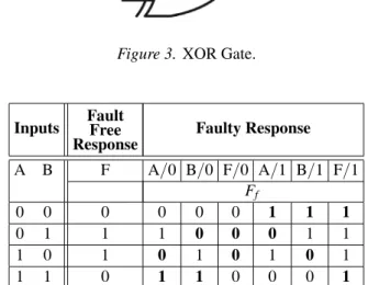
In order to illustrate how SSA fault model can be used to detect defects and possibly use the patterns to locate them, we shall use a 2-input XOR gate. Figure 3, Table 1 shows the function of an XOR gate under various conditions. Col-umn 2 of the table shows the normal response for fault free nodes, whereas column 3 upwards show faulty responses of the gate under faulty conditions. A fault is said to have occurred when the circuit’s normal response is different from the faulty response for the same set of in-put combinations i.e.F =Ff. This can also be
shown as expression(11):
F⊕Ff =1.
With the above expression in mind and closely looking at the table, we realize that faults are not always observable. For instance, with lines A/0, for input combinations 00 and 01F =Ff.
The only time the fault free response differs from the faulty response was when the input combinations AB=10 and AB=11 were applied on the circuit. These input combinations can be considered as the test pattern that detects line
Figure 3.XOR Gate.
Inputs FaultFree
Response Faulty Response
A B F A/0 B/0 F/0 A/1 B/1 F/1 Ff
0 0 0 0 0 0 1 1 1
0 1 1 1 0 0 0 1 1
1 0 1 0 1 0 1 0 1
1 1 0 1 1 0 0 0 1
A stuck-at-0. Because the two patterns detect A/0, either AB=10 or AB=11 can be chosen as the test pattern. Let us now consider faults that are detected by specific input combinations.
AB= 00 detects A/1, B/1 and F/1 01 detects A/1, B/0 and F/0 10 detects A/0, B/1 and F/0 11 detects A/0, B/0 and F/1
From the above we can see that the same in-put combination detects more than one fault. The first test pattern from the above is AB=00 which covers faults A/1, B/1 and F/1. The next pattern is 01 which detects A/1, B/0 and F/0. With these two patterns we have detected five faults namely A/1, B/0, B/1, F/0 and F/1. We are left with one fault i.e. A/0 to be detected. Any of the patterns AB=10 or AB=11 detects this fault. The set of test vectors that will detect all SSA faults for a 2-input XOR gate are: 00, 01 and 11. This means that if we want to test a 2-input XOR gate, it is sufficient to apply all three of these patterns on the inputs of the gate. The fault coverage in this case is 100%. It is important to observe that this example is a triv-ial one indeed, an oversimplification of testing and test pattern generation procedure.
In practice it is a more daunting task as we have to deal with circuits with millions of gates and different interconnection structures. Test pat-tern generation for sequential circuits is very tedious and less straightforward than for com-binational circuits. There are many techniques for test pattern generation, but their discussion is beyond the scope of this paper.
4.4. Fault Coverage, Yield and Defect Level
Fault coverage is a measure employed generally to determine the quality of tests. It is expressed as a ratio of faults detected (covered)by a test pattern to the total number of faults possible for a given fault model. Because of the difficulty in testing ICs exhaustively, some of the faulty ones may escape detection, leading to yield and de-fect level problems. Process yield is a fraction of the manufactured ICs that is defect-free. The process yield is approximated by the ratio of the good ICs to the total number of ICs. Process variations, such as impurities in wafer material and chemicals, dust particles on masks or in
the projection system, mask misalignment; in-correct temperature control, etc. affect the pro-cess yield. It suffices to note that testing can-not improve process yield. However, process diagnosis and correction can improve process yield. This method involves locating defects in the failed parts and tracing them to specific causes, such as defective material, faulty ma-chines, incorrect human procedures, etc. Once the cause is eliminated, the yield improves. When some of the faults escape detection for some components or parts the defect level in-creases. Defect level is the fraction of faulty chips among the chips that pass the test, ex-pressed as parts per million (ppm). A defect level of 100 ppm or lower represents high qual-ity. This means that among the so-called good parts or ICs there are bad ones. It is a well known fact that the quality is a function of user’s satisfaction. To a user the highest quality prod-uct is one that meets requirements at the lowest possible cost. Testing (functional) checks to ensure that final product conforms to its require-ments and the reduction of cost is achieved by enhancing the process yield. The fault coverage (FC) and yield (Y) are given by expressions (12) and (13) respectively. The relationships betweenFC,Yand defect level(DL)are shown in expression(13):
FC =m/n (12)
Y = (1−p)n (13)
DL=1−Y(1−FC) (14)
where:
nis the total number of faults
mis the number of detected faultsm≤n pis the probability of any fault occurring. The following assumptions were made. 1. Stuck-at-fault(SAF)model is assumed, 2. The probability(p)of any fault occurring is
independent of the occurrence of any other fault. That is to say that the faults are mutu-ally exclusive.
5. Making Designs Testable
Testing is an expensive activity in terms of generating the test vectors and their applica-tion to the digital circuit under test. Because of the complexity of testing processes, design for testability(DTF)approach was developed. This design approach is aimed at making digi-tal circuits more easily testable such that these circuits are more controllable and observable by embedding test constructs into the design. There is no formal definition for testability. An interesting attempt was given in [9]as: “A dig-ital IC is testable if test patterns can be gener-ated, applied, and evaluated in such a way as to satisfy predefined levels of performance (e.g., detection, location, application)within a prede-fined cost budget and time scale”. One of the key words is “cost”. It is probably the cost of testing that deters semiconductor manufacturers from doing as much testing as is really needed to ensure reliable products[10].
There are many facets to this cost, such as the cost of:
1. Test pattern generation (automatic and/or manual)time. Test pattern generation is an NP-complete problem since it is difficult to find a polynomial solution.
2. Fault simulations and generation of fault lo-cation information,
3. Test equipment(Automatic Test Equipment). 4. Test application which includes the process
of accessing appropriate circuit lines, pads or pins, followed by application of test vectors and comparison of the captured responses with those expected; time required for de-tecting and/or isolating a fault.
5. Undetectable faults; unpredictable produc-tion schedules and an uncertain level of prod-uct quality delivered to the customer. When many actual faults are not detected by the derived tests, it is often reflected in terms of loss of customers.
The cost associated with undetected fault could be high, see Figure 1, but sometimes difficult to quantify. Although this fault is difficult to quantify, it influences the other costs by impos-ing high fault coverage requirement to ensure that fault escape is kept below an acceptable threshold[11].
In view of the fact that these costs can be exorbi-tant and in most cases exceed design costs, it is
therefore, necessary to keep them within accept-able limit[2]. And this is the reason why design for testability has become imperative. It is a proven way of reducing testing costs. A fault is testable if there exist a well-specified proce-dure to expose it, which can be implemented with a reasonable cost using current technolo-gies. And a circuit is testable with respect to a fault set when each and every fault in this set is testable. As there is price for everything in this world, DFT carries its own penalty – silicon real estate and performance penalties. This is mainly because of the extra circuitry employed for implementing the DFT.
Testability, on the other hand, is introduced at the design stage, where it dramatically lowers the cost of test and the time spent at test. Prop-erly managed, testability heightens your assur-ance of product quality and smoothes produc-tion scheduling.
5.1. DFT at the Design Stage
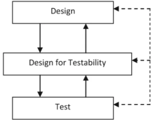
Modern design approach has brought test en-gineering closer to the design activities in that the test program development for an electronic circuit occurs at an early stage in the product development process and requires a basis in de-sign. This overcomes the problems encoun-tered when design and test activities were sep-arate and distinct, an unnecessary barrier be-tween two interrelated activities. In this DFT approach, test activities can influence how a de-sign is created by identifying testability issues and improving test access to specific circuitry within the design. Specialist engineers in both design and testing are supported by a generalist DFT engineer, shown in Figure 4, who bridges
the gap between them. The need for special-ists is based on the need for in-depth knowledge of specific design and test issues, roles which a single person could not realistically be expected to undertake. [5]
5.2. DFT Methodology
There are several methods of making designs testable. None of these methodologies can solve all VLSI testing problems nor can a single tech-nique guarantee effectiveness of testing for all kinds of circuits. Generally, DFT techniques have the capability to increase the circuit real estate on chip, which results in complexity of logic circuits. Increased complexity leads to increase in power consumption and decrease in yield. With all these challenges in mind, there is a need to select a technique for a particular kind of circuit that balances these trade-offs ( bene-fits and challenges). If a circuit is modified to increase its testability by the addition of extra circuitry, it therefore means that another mode of operation apart from the normal mode has been included. This new mode of operation is called test mode. In this mode the circuit is con-figured for testing alone. DFT methods include the following:
• Ad-hoc methods • Scan, full and partial • Boundary scan
• Built-In Self-Test(BIST)
The goal of DFT is to increase controllabil-ity, observability and/or predictability of a cir-cuit. The DFT discipline started with the ad-hoc technique which involves the insertion of test points, counters/shift registers, partitioning of large circuits, logical redundancy and breaking of global feedback paths. Many of these ad-hoc techniques were developed for printed circuit boards and some are applicable to IC design. These methods are referred to as ad hoc(rather than algorithmic)because they do not deal with a total design methodology that ensures ease of test generation, and they can be used at the de-signer’s option where applicable. The detailed description of these techniques can be found in [8]. Scan path is a scheme that facilitates the testing of finite state machines (FSM). Auto-matic test pattern generation for sequential cir-cuits is very tedious and in most cases do not
achieve the required test coverage. This arduous task is as a result of the difficulty in controlling and observing the inputs and output states of the flip flops respectively. In this technique the flip flops(FF)or latches are designed and struc-tured in such a way that allows the circuit to be operated in either of the two modes(normal or scan). Figure 5 shows the structure of the FFs when the circuit is operated in the normal mode.
Figure 5.General model of FSM.
In the test or scan mode, all the FFs are discon-nected and reconfigured as one or more shift registers called scan chains or scan registers. In the test mode all the state inputs(y1,y2, . . . ,yk)
become pseudo-primary inputs to the circuit. The state inputs to the combinational circuit are the present states of the FFs and the state outputs of the combinational circuit(Y1,Y2, . . . ,Yk)are
the next states of the FFs. When developing tests for the FSM, you assume that there is only combinational circuit with the following inputs:
x1,x2, . . . ,xn and y1,y2, . . . ,yk; and outputs:
z1,z2, . . . ,zmandY1,Y2, . . . ,Yk.
times to capture the results. This configuration makes the pseudo primary inputs as control in-puts and the input (pseudo outputs)to a FF an observation point. To switch between normal operation and shift modes, each flip-flop needs additional circuitry to perform the switch. Boundary scan method was developed primarily for the testing of circuit boards and is defined by the core reference IEEE standard 1149.1-2001 “Test Access Port and Boundary-Scan Archi-tecture”. The idea to bring back the access to device pins by means of an internal serial shift register around the boundary of the device is accredited to European test engineers under the aegis JETAG (Joint European Test Action Group). When North American test engineers joined the group it was named JTAG(Joint Test Action Group). It was this group that con-verted the ideas into an International standard, the IEEE 1149.1-1990 Standard first published in April 1990. The ICs that are compliant to this standard must incorporate extra hardware (Shift-Registers – Boundary scan registers) to facilitate communication between them and the board during testing. This idea is illustrated in Figure 6.
Figure 6.Generic boundary scan architecture.
It is important to note at this point that the use of boundary scan has found their ways in internal testing and running of BIST. Apart from BISTs, boundary scan is very useful in testing System on chips (SoC) in a new testing environment that enables systems with IP cores to be easily tested.
Up to this point the techniques that require ex-ternal generation and application of test patterns by an external device like automatic test equip-ment(ATE) have been considered. BISTs are true DFT technique. It encompasses test gener-ation, test application and response verification. It is very useful for current technology which requires testing at speed with due consideration to interconnect delays. Where SAF model fails, BIST succeeds. BISTs can detect faults that otherwise would not have been detected using SAF models – delay faults. In this methodology, test patterns are generated and test responses are analyzed on-chip.
The test pattern generator (TPG) in a BIST is implemented with linear feedback shift regis-ters(LFSR) [2]which is a finite state machine. It is a shift register with feedback from the last stage and other stages. The outputs of the flip-flops form the test pattern. It consists of FFs and XOR gates. The number of FFs and XOR gates depends on the characteristic polynomial of the LFSR. The generic BIST architecture is shown in Figure 7. The responses of the circuit under test(CUT)could be large. Consequently the output responses are compacted by the re-sponse compactor(RC)to generate a signature at the end of the test application since the inter-est has been on how the circuit responded to the various test patterns from the LFSR.
Figure 7.General BIST architecture.
6. A Simple Example of DFT Technique Using Scan Chain Methodology
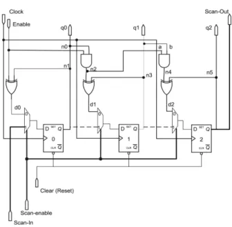
As earlier mentioned, DFT techniques help in-crease the testability of fabricated circuit by en-hancing the controllability and observability of various nets of the circuit. To show how DFT enhances the testability of a circuit, let us con-sider a simple counter circuit as shown in Fig-ure 8. The circuit is divided into two parts: com-binational and sequential. The part containing the AND and XOR gates is the combinational circuit. The circuit has the following parts ac-cessible to the outside world: outputs q0 to q2, Clock, Enable and Clear inputs. As it is now, it will be difficult to properly test this circuit since you have no access to the internal nodes. If node n4 is stuck-at 1 or 0, there is no way one can know about this since one can neither control nor observe the node.
Figure 8.A simple counter circuit.
To make this circuit testable one has to introduce some extra hardware and increase the number of the input and output ports. Firstly, replace the three flip-flops(FF)with a different type of FFs that has a multiplexer at the D input. By this action, additional three ports have been added namely: Scan-In, Scan-Out and Scan enable. The new sequential circuit is shown in Figure 9. With the new configuration the FFs form a shift register. Bit sequence can be shifted into the FFs through the in input pin with the scan-enable signal set to high (logic 1)and the bits shifted out of the shift register can be observed
Figure 9.A simple counter circuit with DFT.
at the scan-out output pin. Under normal op-eration of the sequential circuit the scan-enable signal is set to low(logic 0). The only change here is that our circuit can operate in two modes – normal and test modes. One can now develop and generate tests pattern for the combinational part to test the whole circuit the FFs inclusive. Let us assume that the node n4 is stuck-at-0. You can control input lines ‘a’ and ‘b’ to logic ‘1’ and set n5 to ‘0’ and observe the output at scan-out pin. The purpose of setting n5 to ‘0’ is to propagate the fault n4 stuck-at-0 to the output d2 of the XOR gate. Let us now look at how one can detect the fault stuck-at-0 at line n4. Reset all FFs to 0
Set line ‘a’=1 by setting enable input=1 and n0=0(FF0 was earlier reset to 0)d0=1, subsequently FF0 output will be set to 1. With enable=1 and FF0=1→n2=1 Set line ‘b’=1, by setting FF1 output to 1.
If n2=1, then d1=1→FF1=1. Set n5=0. Since n5 is the same as the FF2
output n5 is already 0.
With the above settings you are supposed to have logic 1 at the output. If, however, the output is 0, then node n4 is stuck-at-0.
testing of this circuit has become a combina-tional problem rather than a sequential one. The down side is that the circuit area has been in-creased, though not significantly. In[3], it was observed that scan-based DFT technique leads to long test application time and it is less useful for at-speed testing.
7. Conclusion
In this paper it has been shown that product quality depends to a greater extent on the thor-oughness of verification and testing processes during its development. Testing of digital com-ponents/system is time consuming, expensive and can negatively affect time to market. The example given in this paper has clearly demon-strated that design for testability greatly eases the process of testing without a serious con-sequence on the area and delay issues of the would-be chip.
References
[1] A D&T Roundtable: System Test – What, Why and How? IEEE Design and Test of Computers 7(1990), 66–72.
[2] D. SCHMID, H. WUNDERLICH, ET AL, Integrated
Tools for Automatic Design for Testability. In Con-ference on Tool Integration and Design Environ-ments,(1988)pp. 233–258. Amsterdam: Elsevier Science Publishers B. V.(North Holland), IFIP.
[3] H. FANG, K. CHAKRABARTY, H. HIDEOFUJIWARA, RTL DFT Techniques to Enhance Defect Coverage for Functional Test. Journal of Electronic Test-ing: Theory and Applications (JETTA)26(2010), 151–164.
[4] L. YU-TING, D. WILLIAMS, T. AMBLER,
Cost-effective designs of field service for electronic systems. In International Test Conference,(2005)
pp. 460–467.
[5] I. GROUT,Digital Systems Design with FPGAS and
CPLDS. Newnes-Elsevier, London, 2008.
[6] M. A. BREUER, A. D. FRIEDMAN,Diagnostics and Reliable Design of Digital Systems. Computer Sci-ence Press, New York, 1976.
[7] TAIWANSEMICONDUCTORMANUFACTURINGCOM -PANY(TSMC),(2010)Move to 20nm Process.,
http://www.tsmc.com/tsmcdotcom/PRListing NewsAction.do?action=detail&newsid=4741 &language=E
Accessed 14 May 2010.
[8] M. ABRAMOVICI, M. A. BREUER, A. D. FRIEDMAN,
Systems testing and testable design. IEEE Press, New York, 1990.
[9] R. G. BENNETTS,Design of Testable Logic Circuits.
Addison-Wesley, Reading, MA, 1984.
[10] S. MOURAD, Y. ZORIAN,Principles of Testing Elec-tronic Systems. Wiley, New York, 2000.
[11] N. JHA, S. GUPTA,Testing of digital systems. Cam-bridge University Press, New York, 2003.
[12] R. BRAYTON, J. CONG, NSF Workshop on EDA:
Past, Present, and Future(Part 2).IEEE Design and Test Computers27(2010), 62–73.
[13] K. Y. CHO, S. MITRA, E. J. MCCLUSKEY, Gate
ex-haustive testing. InInternational Test Conference,
(2005)pp. 777–183.
Received:June, 2011
Revised:November, 2012
Accepted:November, 2012
Contact address:
Christopher Umerah Ngene Department of Computer Engineering University of Maiduguri Nigeria