FULL CUSTOM IMPLEMENTATION OF AN 8B/10B ENCODER WITH
A MODIFIED CODING TABLE
B. Koteswar Rao* Dr S. Kishore Reddy**
ABSTRACT
This paper presents a design of 8B/10B encoder with a modified coding table. The proposed
encoder has been designed based on a reduced coding table with a modified disparity control
block. After being synthesized using CMOS 0.18μm process, the proposed encoder shows the operating frequency of 343 MHz and occupies the chip area of 1886 μm2 with 189 logic
gates. It consumes 2.74mW power. Compared to conventional approaches, the operating
frequency is improved by 25.6% and chip area is decreased to 43%.
IJREAS
Volume 3, Issue 1 (January
2013)
ISSN: 2249-3905
I.
INTRODUCTION
The 8B/10B encoder is used to generate ample data transition for facilitating a clock recovery function in the various networks. Also it provides a DC balance by trying to equalize the
number of '0' and '1' in the data stream. There are extra codes called as special code group for identifying the data sequence boundary in the data recovery unit. Thus the 8B/10B encoding technique is used in various high-speed serial data transmission standards, which are Fiber channel, Gigabit Ethernet, Server Net, and Infiniband. As the demand of high-speed communication increases, the 8B/10B encoding block is also required to be operating in giga bits per second range. Therefore it is necessary to have a more efficient and high speed operating 8B/10B encoder/decoder design. Fig. 1 shows the 8B/10B encoder/decoder block in communication system.
Most popular, de facto standard, 8B/10B encoder design is based on the scheme proposed by IBM [1]. However, the logic implemented based on the conventional encoding table needs many logic depth, thus the operating speed can be limited. To overcome this speed issue, new encoding approaches were suggested. By introducing pipelining, logic optimization, and utilizing a memory tables for coding and disparity inside ASIC or FPGA were investigated. In this paper, we present a design of 8B/10B encoder by coding table reduction. The proposed encoder has a simplified coding table using adder compared to conventional coding table and has a modified disparity control block. The paper describes the proposed encoder architecture first and shows the design results.
II.
ARCHITECTURE
A. Conventional 8B/10B Encoder
Fig. 2 shows a conventional 8B/10B encoder. Encoding starts by dividing two different sub-blocks, which are 5B/6B encoder (inputs A to E) and 3/4B encoder (inputs F to H). After disparity is checked, the encoding switches set the final encoded output values. The disparity control block is to make DC balance on the data stream by equalizing the number of '0' and '1'. The 'K' input is for special character that is used for data packet boundary detection. The encoding table for the conventional encoder is given in Table I.
Figure1. 8B/10B encoder/decoder block in communication system.
Figure2. Block diagram of conventional 8B/10B encoder.
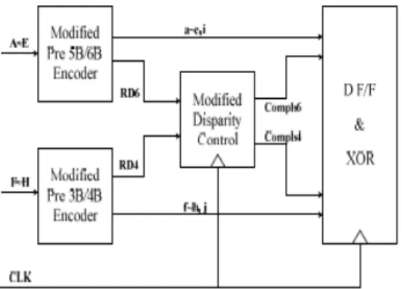
B. Proposed 8B/10B Encoder
The proposed block diagram for a modified 8B/10B encoder is shown in Fig. 3. The blocks
look similar to the conventional one, but at input side the pre encoder blocks are modified and the special character inputs are omitted. Instead, the special character case will be handled in the pre encoder blocks.
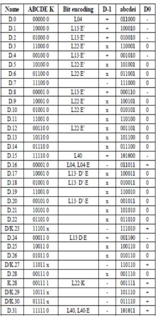
As indicated in the Table I in the original 5B/6B encoding, the encoded outputs (denoted as 'abcd') are not changed except input data 'A' through 'D' are all zero or one. From this point, by classifying the summing values of the input bit patterns, the original encoding table can be reduced. The simplified encoding table is given in Table II.
IJREAS
Volume 3, Issue 1 (January
2013)
ISSN: 2249-3905
The codes of D.24 and K.28 in the original table are not applied by the reduction algorithm. The special cases (D.24, K.28 in the original table) should be handled in the modified encoding scheme because in case of D.24 (=00011) input, the summing value gives '1' at ABCD. Therefore the outputs are not changed. But depending on previous bit sequence of 'f' and 'g', the bit length of consecutive '1' or '0' could be more than five, which is not allowed in
the 8B/10B encoder. In this case it is encoded to '001100' for DC balance. In addition to that, in the case of K.28, the encoded output 'i' should be changed from '0' to '1' for representing comma value. Therefore additional logic for handling D.24 and K.28 cases is required. The additional logic, however, has a little overhead in logic size.
TABLE II. MODIFIED 5B/6B ENCODING TABLE
IJREAS
Volume 3, Issue 1 (January
2013)
ISSN: 2249-3905
C. Modified Disparity Control Block
Table V shows an original disparity coding tables. In conventional encoding table, the complemented output and current disparity value are generated after checking the previous disparity value. In the modified scheme, however, the encoded output and current disparity value are generated without considering the previous disparity value. By checking the current
running disparity and the outputs from 5B/6B and 3B/4B encoding block with current disparity, the next disparity value and the execution of complementing the final output are determined in the modified disparity block. The block diagram of the modified disparity control is shown in Fig. 4. Running disparity outputs of CurRD6 and CurRD4 are coming from the modified Pre 5B/6B encoder and Pre 3B/4B encoder, respectively.
Depending on previous and current disparity outputs, the disparity control determines whether to complement the pre encoded 5B/6B and 3B/4B outputs. The whole operation of the disparity control is summarized in Table VI.
PreRD and CurRD in Table VI stand for previous and current running disparities of encoded output. And when 'compls' is equal to '1', then complementing the encoded output is executed. The Next RD is next running disparity used as Pre RD after one clock cycle in the 5B/6B disparity check block. In order to decide the complement the pre encoded outputs, the previous 4B encoded outputs are used as shown in Fig. 4.
For K28.3 code, the disparity value in the previous encoding stage is minus (-) and the disparity value of current encoding stage becomes plus (+). Then the sign of 'compls4' is '0' and generate the encoded data without complementing action. As a result the encoded result can have a run length of 6. This is not allowed in the 8B10B encoding scheme. In order to solve the problem, the logic has to set the 'Compls4' for K28.3 and K28.2 code and the 'Compls6' for D7.7.P7 code to be '1' after checking the disparity.
III.
PERFORMANCE ANALYSIS
The proposed encoder has been design using Verilog and simulated using the VCS. Synthesis and P&R (Place and Route) are performed by the Synopsys Design Compiler and the Astro, respectively, using the CMOS 0.18um technology library. Fig. 6 shows the layout of the proposed algorithm.
As an example, the expected encoded output '0110010010' (2th byte in output_10b signal) is generated for the D6.4 code (='01100001': first byte in input_8b signal). And after decoding this value by a decoder, original input value is exactly recovered.
For the performance comparison, we also designed a Encoder based on the original IBM's encoding table. In Table VII, the performance comparison to original IBM design is given. It
shows that the cell area has been increased to 2.1%, but the operating frequency is improved by 25.6% compared to conventions. The 8B/10B encoder proposed by Xilinx [5] has been also compared. The operating frequency is improved by 3.9%, the cell area has been decreased to 43% compared to the Xilinx approach.
The operating frequency improvement has been achieved by the modified disparity algorithm comparing the current disparity rather than previous disparity value in conventions. The Xilinx’s encoder used a state-machine based operation to increase the operating speed. In terms of power consumption, the proposed scheme shows about 40% power reduction compared to IBM’s. The Xilinx’s encoder shows the lower power consumption but it needs a latency of five clock cycles. As a result, the proposed 8B/10B encoder shows the overall performance improvement in the operating frequency, chip area, and power consumption.
IV.
CONCLUSION
IJREAS
Volume 3, Issue 1 (January
2013)
ISSN: 2249-3905
ACKNOWLEDGMENT
This work was supported by "System IC 2010" project of Korea Ministry of Knowledge Economy. Hardware and software tools were supported by IT-SOC and the IDEC program.
REFERENCES
[1] A.X.Widmer, "A DC-balanced, Partitioned-Block, 8B/10B transmission Code", IBM J. Res. Develop, vol. 27, pp.440-451, September, 1983.
[2] H. Lee, S. Park, "High speed 8B/10B encoder/decoder design by Logic Reduction",
2003 SoC Design Conf., pp.910-913, Nov, 2003.
[3] Actel, "Implementing an 8b/10b Encoder/Decoder for Gigabit Ethernet", Application Note, Oct, 1998.