CHAPTER 3
Motor Control
3.1 AC Motor Control
3.2 DC Motor Control
3.3 Stepper Motor Control
3.1.1 Noiseless A.C. Motor Control: Introduction to a 20 kHz
System
Controlling an a.c. induction motor by the technique of
sinewave-weighted pulse-width modulation (PWM)
switching gives the benefits of smooth torque at low speeds, and also complete speed control from zero up to the nominal rated speed of the motor, with only small additional motor losses.
Traditional power switches such as thyristors need switching frequencies in the audible range, typically between 400 and 1500Hz. In industrial environments, the small amount of acoustic noise produced by the motor with this type of control can be regarded as insignificant. By contrast, however, the same amount of noise in a domestic or office application, such as speed control of a ventilation fan, might prove to be unacceptable.
Now, however, with the advent of power MOSFETs,
three-phase PWM inverters operating at ultrasonic
frequencies can be designed. A three-phase motor usually makes even less noise when being driven from such a system than when being run directly from the mains because the PWM synthesis generates a purer sinewave than is normally obtainable from the mains.
The carrier frequency is generally about 20kHz and so it is far removed from the modulation frequency, which is typically less than 50Hz, making it economic to use a low-pass filter between the inverter and the motor. By removing the carrier frequency and its sidebands and harmonics, the waveform delivered via the motor leads can be made almost perfectly sinusoidal. RFI radiated by the motor leads, or conducted by the winding-to-frame capacitance of the motor, is therefore almost entirely eliminated. Furthermore, because of the high carrier frequency, it is possible to drive motors which are designed for frequencies higher than the mains, such as 400Hz aircraft motors.
This section describes a three-phase a.c. motor control system which is powered from the single-phase a.c. mains. It is capable of controlling a motor with up to 1kW of shaft output power. Before details are given, the general principles of PWM motor control are outlined.
Principles of Pulse-Width Modulation
Pulse-width modulation (PWM) is the technique of using switching devices to produce the effect of a continuously varying analogue signal; this PWM conversion generally has very high electrical efficiency. In controlling either a three-phase synchronous motor or a three-phase induction motor it is desirable to create three perfectly sinusoidal current waveforms in the motor windings, with relative phase displacements of 120˚. The production of sinewave
power via a linear amplifier system would have low efficiency, at best 64%. If instead of the linear circuitry, fast electronic switching devices are used, then the efficiency can be greater than 95%, depending on the characteristics of the semiconductor power switch.
Fig.1 Half-bridge switching circuit
Fig.2 Waveforms in PWM inverter (a) Unmodulated carrier
(b) Modulated carrier (c) Current in inductive load
The half-bridge switching circuit in Fig.1 is given as an example: the switches can be any suitable switching semiconductors. If these two switches are turned on alternately for equal times, then the voltage waveform across the load is as shown in Fig.2a. The mean value of this waveform, averaged over one switching cycle is 0. This square wave with a constant 50% duty ratio is known as the ’carrier’ frequency. The waveform in Fig.2b shows the effect of a slow variation or ’modulation’ of the duty ratio; the mean voltage varies with the duty ratio. The waveform of the resultant load current depends on the impedance of the load Z. If Z is mainly resistive, then the waveform of the current will closely follow that of the modulated square wave. If, however, Z is largely inductive, as with a motor winding or a filter choke, then the switching square wave
V/2 V/2 + + Z -V/2 V/2 0 0 -V/2 V/2 0 I (a) (b) (c)
will be integrated by the inductor. The result is a load current waveform that depends mainly on the modulation of the duty ratio.
If the duty ratio is varied sinusoidally in time, then the current in an inductive load has the form of a sinewave at the modulation frequency, lagging in phase, and carrying ripple at the switching frequency as shown in Fig.2c. The amplitude of the current can be adjusted by controlling the depth of modulation, that is, the deviation of the duty ratio from 50%. For example, a sinewave PWM signal which varies from 5% to 95%, giving 90% modulation, will produce a current nine times greater than that produced by a signal which varies only from 45% to 55%, giving only 10% modulation.
For three-phase a.c. motor control, three such waveforms are required, necessitating three pairs of switches like those shown in Fig. 1, connected in a three-phase bridge. The inductance required to integrate the waveform can usually be provided by the inductance of the stator windings of the motor, although in some instances it might be provided by the inductance of a separate low-pass filter. The modulations in the three switching waveforms must be maintained at a constant relative phase difference of 120˚, so as to maintain motor current sinewaves which are themselves at a constant 120˚ phase difference. The modulation depth must be varied with the modulation frequency so as to keep the magnetic flux in the motor at approximately the design level.
In practice, the frequency of the modulation is usually between zero and 50Hz. The switching frequency depends on the type of power device that is to be used: until recently, the only devices available were power thyristors or the relatively slow bipolar transistors, and therefore the switching frequency was limited to a maximum of about 1
kHz. With thyristors, this frequency limit was set by the need to provide forced commutation of the thyristor by an external commutation circuit using an additional thyristor, a diode, a capacitor, and an inductor, in a process that takes at least 40µs. With transistors, the switching frequency was limited by their switching frequency and their long storage times.
In this earlier type of control circuit, therefore, the ratio of carrier frequency to modulation frequency was only about 20:1. Under these conditions the exact duty-ratios and carrier frequencies had to be selected so as to avoid all sub-harmonic torques, that is, torque components at frequencies lower than the modulation frequency. This was done by synchronising the carrier to a selected multiple of the fundamental frequency; the HEF4752V, an excellent IC purpose-designed for a.c. motor control, uses this particular approach. The 1kHz technique is still extremely useful for control of large motors because whenever shaft output powers of more than a few kW are required, three-phase mains input must be used, and there are, as yet, few available switching devices with combined high voltage rating, current rating, and switching speed.
However, using MOSFETs with switching times of much less than 1µs, the carrier frequency can be raised to the ultrasonic region, that is, to 20kHz or more. There are obvious system benefits with this higher frequency, but there are also several aspects of PWM waveform generation that become easier. It is possible to use a fixed carrier frequency because the sub-harmonics that are produced as a result of the non-synchronisation of the carrier frequency with a multiple of the fundamental are insignificant when the ratio of the carrier frequency to the fundamental frequency is typically about 400:1.
To maintain good waveform balance, and thus avoid any d.c. in the motor, and therefore also avoid parasitic torques, a digital waveform generation technique is appropriate. The waveform can be stored as a ’look-up’ table of numbers representing the sinewave. To generate the three phases, this table can be read at three points that have the correct 120˚ phase relationship. The numbers taken from the table
represent the duty ratios corresponding to 100%
modulation: these numbers can then be scaled down by multiplication or some equivalent technique to give the correct duty-ratio numbers for the modulation depth required.
The speed of the motor is controlled by the rate at which the reading pointers scan the look-up table and this can be as slow as desired. If the pointers are stationary, then the system will be ’frozen’ at a particular point on the three-phase sinewave waveform, giving the possibility of obtaining static torque from a synchronous motor at zero speed. The rate at which the numbers are produced by this read-out process from the look-up table is constant and determines the carrier frequency.
To convert these three simultaneous parallel digital numbers into time lengths for pulses, three digital counters are needed. The counters can be designed to give double-edged modulation, such that both the leading edge and the trailing edge of each pulse move with respect to the unmodulated carrier. The line-to-line voltage across the load will have most of its ripple at a frequency of twice the switching frequency, and will have a spectrum with
minimum even harmonics and no significant component below twice the switching frequency. Motor ripple current is therefore low and motor losses are reduced.
There is a further advantage to be obtained from the high ratio of carrier to modulation frequency: by adding a small amount of modulation at the third harmonic frequency of the basic fundamental modulation frequency, the maximum line-to-line output voltage obtainable from the inverter can be increased, for the following reason. The effect of the third harmonic on the output voltage of each phase is to flatten the top of the waveform, thus allowing a higher amplitude of fundamental while still reaching a peak modulation of 100%. When the difference voltage between any two phases is measured, the third harmonic terms cancel, leaving a pure sinewave at the fundamental frequency. This allows the inverter output to deliver the same voltage as the mains input without any significant distortion, and thus to reduce insertion losses to virtually zero.
Overview of a practical system
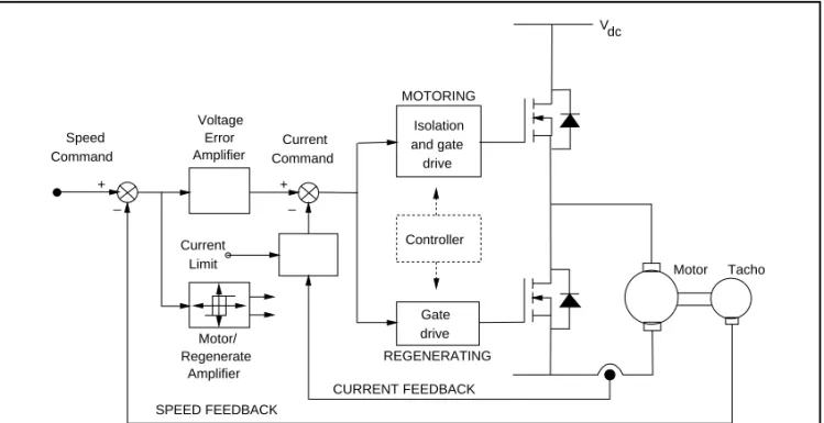
The principles outlined above are applied to a typical system shown in Fig.3. The incoming a.c. mains is rectified and smoothed to produce about 300V and this is fed to the three-phase inverter via a current-sensing circuit. The inverter chops the d.c. to give 300V peak-to-peak PWM waves at 20kHz, each having low-frequency modulation of its mark-space ratio. The output of the inverter is filtered to remove the 20kHz carrier frequency, and the resultant sinewaves are fed to the a.c. motor.
The six switches in the inverter are under the command of a waveform-generation circuit which determines the conduction time of each switch. Because the control terminals of the six switches are not at the same potential, the outputs of the waveform-generation circuits must be isolated and buffered. A low-voltage power supply feeds the signal processing circuit, and a further low-voltage power supply drives a switch-mode isolating stage to provide floating power supplies to the gate drive circuits.
Signal processing
Fig.4 shows a block diagram of the circuit which generates the PWM control signals for the inverter. The input to the system is a speed-demand voltage and this is also used for setting the required direction of rotation: the analogue speed signal is then separated from the digital direction signal. The speed-demand voltage sets the frequency of the voltage-controlled oscillator (VCO). Information to determine the modulation depth is derived from the speed-control signal by a simple non-linear circuit and is then converted by an analogue-to-digital converter into an 8-bit parallel digital signal.
A dedicated IC, type MAB8051, receives the clock signals from the VCO, the modulation-depth control number from the A/D converter, the direction-control logic signal, and logic inputs from the ’RUN’ and ’STOP’ switches. By applying digital multiplication processes to internal look-up table values, the microcomputer calculates the ’on-time’ for each of the six power switches, and this process is repeated at regular intervals of 50µs, giving a carrier frequency of 20kHz. The pulses from the VCO are used for incrementing the pointers of the look-up table in the microcomputer, and thus control the motor speed.
The output signals of the microcomputer are in the form of three 8-bit parallel numbers: each representing the duty-ratio for the next 50µs switching cycle for one pair of inverter switches, on a scale which represents 0% to 100% on-time for the upper switch and therefore also 100% to 0% on-time for the complementary lower switch. A dedicated logic circuit applies these three numbers from the microcomputer to digital counters and converts each number to a pair of pulse-widths. The two signals produced for each phase are complementary except for a small ’underlap’ delay. This delay is necessary to ensure that the switch being turned off recovers its blocking voltage before its partner is turned on, thus preventing ’shoot-through’.
Other inputs to the microcomputer are the on/off switches, the motor direction logic signal, and the current-sensing signal. Each input triggers a processor interrupt, causing the appropriate action to be taken. The STOP switch and the overcurrent sense signals have the same effect, that of causing the microcomputer to instruct all six power switches in the inverter to turn off. The RUN switch causes the microcomputer to start producing output pulses. Any change in the direction signal first stops the microcomputer which then determines the new direction of rotation and adjusts its output phase rotation accordingly.
D.C. link and power supplies
The d.c. link and the low-voltage power supplies for the system are shown in Fig.5. The high voltage d.c. supply for the inverter is derived from a mains-fed bridge rectifier with a smoothing capacitor; the capacitor conducts both the 100Hz ripple from the rectified single-phase mains, and also the inverter switching ripple. A resistor, or alternatively a thermistor, limits the peak current in the rectifier while the capacitor is being charged initially. This resistor is shorted out by a relay after a time delay, so that the resistor does not dissipate power while the motor is running. As a safety measure, a second resistor discharges the d.c. link capacitor when the mains current is removed.
One of the d.c. link lines carries a low-value resistor to sense the d.c. link current. A simple opto-isolation circuit transmits a d.c. link current overload signal back to the signal processing circuit.
The logic circuitry of the waveform generator is powered conventionally by a 50Hz mains transformer, bridge rectifier, and smoothing capacitor. The transformer has two secondary windings; the second one provides power to a switched-mode power supply (SMPS), in which there is a switching transistor driven at about 60kHz to switch power through isolating transformers. Rectifying the a.c. outputs from the isolating transformers provides floating power supplies for the inverter gate drive circuits. As will be seen below, one supply is needed for the three ’lower’ power switches (connected to a common d.c. link negative line), but three separate power supplies are needed for the three ’upper’ switches (connected to the three inverter outputs). Thus four isolating transformers are required for the gate supply circuits. For low power systems the gate supplies can be derived directly from the d.c. link without excessive loss.
To prevent spurious turn-on of any inverter switch during the start-up process, the floating power supply to the lower three gate-drive circuits is connected only after a delay. The same delay is used for this as is used for the d.c. link charging-resistor bypass switch.
Fig.6 Signal isolation, gate drive, inverter and filter (one phase of three)
15 V HEF40097 2k2 2k2 10T 20T 47 pF 18 k 1 k c18v 100R FX3848 8 uF 2n2 15 V HEF40097 2k2 2k2 10T 20T 47 pF 18 k 1 k c18v 100R FX3848 8 uF 2n2
Signal isolation, gate drive, and inverter
The most important part of the system is the power inverter and it is the use of MOSFETs, with their short switching times, which makes it possible for the inverter to switch at 20kHz. It is in the area of the drive circuits to the power switches that using MOSFETs gives a saving in the number of components needed. Driving MOSFETs is relatively easy: the total power needed is very small because all that must be provided is the capability to charge and discharge the gate-source capacitance (typically between 1 and 2nF) by a few volts in a short time (less than 100ns). This ensures that the quality of the waveform is not degraded, and that switching losses are minimised.
In this circuit the six pulse outputs from the dedicated logic part of the waveform generator section are coupled to the MOSFET gate driver stages via pulse transformers. (see Fig.6). Each gate drive circuit is powered from one of the four floating power supplies described above. The three ’lower’ stages share a common power supply, as the source terminals of the three ’lower’ MOSFETs are all at the same potential. Each of the three ’upper’ stages has its own floating power supply. The isolated signals are coupled to the gate terminals of the six MOSFETs by small amplifiers capable of delivering a few amperes peak current for a short time. Alternative gate driver circuits may use level shifting devices or opto-couplers. (Refer to "Power MOSFET Gate Drive Circuits" for further details.)
It will be seen from Fig.6 that each MOSFET has two associated diodes. These are necessary because the MOSFETs have built-in anti-parallel diodes with relatively long reverse-recovery times. If these internal diodes were
allowed to conduct, then whenever load current
commutated from a diode to the opposite MOSFET, a large current would be drawn from the d.c. supply for the duration of the diode reverse-recovery time. This would greatly increase the dissipation in the inverter. To avoid this, an external fast epitaxial diode is connected in anti-parallel with the MOSFET. Because the internal diode of the MOSFET has a very low forward voltage drop, a second low-voltage epitaxial diode must be connected in series with each MOSFET to prevent the internal diode from conducting at all. Thus, whenever the MOSFET is reverse-biased, it is the external anti-parallel diode which conducts, rather than the internal one. FREDFETs have internal diodes which are much faster than those of MOSFETs, opening the way for a further cost-saving by omitting the twelve diodes from the 3-phase inverter.
Output low-pass filter
For conventional, lower frequency inverters the size, weight and cost of output filter stages has held back their proliferation. An advantage of the constant high carrier frequency is that a small, economical low-pass filter can be designed to remove the carrier from the inverter output
waveform. Compared with low frequency systems the filter component has been reduced by an order of magnitude, and can often be eliminated completely. In unfiltered systems cable screening becomes an important issue although on balance the increased cost of screening is less than the cost and weight of filter components.
A typical filter arrangement was shown in Fig.6. As an example, for a 50Hz motor-drive the filter would be designed with a corner-frequency of 100Hz, so that the attenuation at 20kHz would be about 46dB. The carrier
frequency component superimposed on the output
sinewave would therefore be only a few mV in 200Vrms. Fig.7 shows the relative spectral characteristics of different types of inverter switching strategies.
Fig.7 Spectral characteristics for different inverter switching strategies
(a) Quasi-square (b) 1kHz, 15 pulse, Synchronous
(c) 20kHz, Non-synchronous
There are two main advantages in supplying the motor with pure sinewave power. First, the motor losses are small, because there is no rms motor current at the switching frequency, and second, there is less radio-frequency interference (RFI), because the switching frequency current components circulate entirely within the inverter and filter and do not reach the outside world.
Advantages of a 20 kHz system
The principal advantages of the system described here are: -Controller and motor are acoustically quiet. -PWM waveform is simple and thus easy to generate.
-Output filter for removal of carrier is economic. -RFI is low because of output filter.
-No snubbers are required on power devices. -High efficiency is easily obtainable. -No insertion loss.
f(Hz) 100 1k 10k 100k Power (W) 1kW 10W 100mW f(Hz) 100 1k 10k 100k Power (W) 1kW 10W 100mW f(Hz) 100 1k 10k 100k Power (W) 1kW 10W 100mW (a) (b) (c)
3.1.2 The Effect of a MOSFET’s Peak to Average Current Rating
on Inverter Efficiency
The control of induction motors using a synthesised sinewave generated using pulse width modulation (PWM) control is becoming increasingly popular. The peak current requirement of switches used for the inverter bridge is based on the maximum current when the output is short circuited. The overcurrent during a short circuit fault is limited by an inductor connected in series with the switches. There is therefore a trade off between the peak current carrying capability of the switch and the size of the inductor. It is demonstrated in this note that the efficiency of the circuit during normal operation of the inverter is affected by the size of this choke. The ratio of peak to average current carrying capability of Philips Powermos is typcially about four. This compares favourably with the typical ratio of Insulated Gate Bipolar Transistors (IGBTs) which is about three.
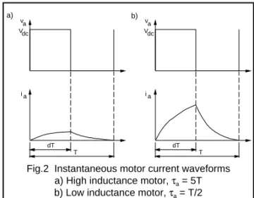
A simplified diagram of the inverter and the windings of the induction motor is shown in Fig. 1. The MOSFETs are driven with a PWM signal as shown in Fig. 2. The voltages at the outputs of each leg of the inverter are smoothed using a low pass filter and the inductance of the motor windings. The system has the following advantages; it uses an induction motor which is relatively cheap and maintenance free and it has the facility for 0 to 100% speed control. The near perfect sinewaves generated by the PWM technique produce a smooth torque, audible noise is reduced and filtering is made easier since MOSFETs make possible the use of switching frequencies above 20 kHz.
Fig. 1 A simplified diagram of the inverter
Fig. 2 PWM drive signal for the inverter MOSFETs
If the output of the inverter is short circuited there will be a rapid rise of current in the switches. To limit this peak current an inductor, Ls,is often connected in each leg of the inverter as shown in Fig 3. The rate of rise of current under short circuit conditions, is then given in equation 1.
(1)
Fig. 3 Inverter bridge leg with dI/dt limiting inductor Vdc 0 Vdc 2 dIT dt= VD Ls
VD
M1
M2
D1
D2
CS
R
S
I motor
0V
I
M1
L
S
When the MOSFETs turn this fault current (ISC) off the energy in the inductor is transferred to a snubber capacitor, CS. The overvoltage across the MOSFETs is given by equation 2.
(2)
The presence of inductor LSaffects the normal operation of the inverter. When the MOSFET M1 in Fig. 3 turns off the diode D2 does not turn on until the voltage across CS is equal to the d.c. link voltage, VD. If the diode did turn on then the rate of rise of current in LSwould be given by equation 3.
(3)
This would be greater than the rate of rise of motor current so IM1> Imotorand the diode would have to conduct in the reverse direction, which is clearly not possible.
During the time when the capacitor CSis charging up to VD, the voltage across LSwill always be such as to increase the current in the bottom MOSFET, IM1. When VCS=VD the voltage across LSwill reverse and IM1will fall. Diode D2 will now turn on. The energy stored in LSwill now be transferred to CS. This energy will subsequently be dissipated in RSand the MOSFET.
If the ratio of peak to average current carrying capability of the switch is large then it follows from equation 1 that LS can be made smaller. This reduces the energy that is
transferred to CSwhen the MOSFETs switch off during normal operation. Hence the efficiency of the inverter is improved.
The short circuit fault current can be limited by connecting an inductor in the d.c. link as shown in Fig. 4. In this case analysis similar to that outlined above shows that the excellent ratio of peak to average current carrying capability of Philips Powermos again reduces the losses in the inverter. It has been shown that components chosen to ensure safe shutdown of inverters for motor drives can have deleterious effects on the efficiency of the inverter. In particular the addition of an inductor to limit the peak current through the semiconductor switches when the output is short circuited can increase the switching losses. The high peak to average current carrying capability of Philips Powermos reduces the size of this choke and the losses it causes.
Fig. 4 Modified inverter circuit to limit short circuit current V=
√
Ls Cs .ISC dIM1 dt = VD−VCS−Vdiode Ls3.1.3 MOSFETs and FREDFETs for Motor Drive Equipment
The paper discusses the properties of the FREDFET, a technology which yields a MOSFET with a very fast built-in reverse diode with properties similar to a discrete fast epitaxial rectifier. It is shown that its characteristics make the device an excellent choice for high frequency bridge leg systems such as 20 kHz AC motor control systems.
Investigations have been carried out in dedicated test circuits as well as in a 20 kHz ACMC system which show that the FREDFET exhibits very low diode losses. It compares favorably with a discrete solution, using two extra diodes to overcome the slow speed of the standard built-in diode, and also with devices from the present standard ranges.
Introduction
The Power MOSFET has inherent in its structure a large built-in diode which is present between the source and drain of the device. Under single switch applications such as forward and flyback converters, this diode isn’t forward biased and consequently its presence can be ignored. In the case of bridge legs, however, this diode is forced into forward conduction and the properties of the diode become of prime importance. The reverse recovery of the built-in diode is relatively slow when compared with discrete fast recovery epitaxial diodes (FRED’s). As a consequence, the currents flowing through the MOSFET and its diode can be high and the losses considerable.
Fig.1. ACMC bridge leg.
These losses can be reduced through the application of two extra diodes as discussed in section 2. A more elegant solution is a MOSFET with a built-in diode which exhibits properties similar to discrete fast epitaxial rectifiers. The FREDFET has been designed to satisfy this requirement. This paper presents the results of studies, carried out with
new FREDFETs, comparing them with both the
conventional MOSFET and the discrete solution.
MOSFETS in half bridge circuits
MOSFETS have gained popularity in high frequency AC motor controllers, since they enable frequencies above 20kHz to be used. The short on-times required in ACMC systems make the use of bipolar devices very difficult, due to the storage times. Both the short switching times and the ease of drive of the MOSFET are essential ingredients in the design of a ultrasonic ACMC. Difficulties can arise, however, when trying to use the built in source to drain diode of the MOSFETs.
One bridge leg of an ACMC is shown in Fig.1. When current is flowing out of the load, MOSFET T1 and freewheel diode D2 conduct alternately. Conversely, when flowing into the load, the current alternates between TR2 and D1. Consider the case when current is being delivered by the load, such that the pair TR1/D2 carries the current. When the MOSFET conducts current, the voltage at the drain is almost zero and the diode blocks. When the MOSFET is turned off by the drive circuit, the inductive load forces the voltage to increase making diode D2 conductive. Associated with conduction of the diode is a volume of stored charge which must be removed as the MOSFET TR1 returns to its on-state.
Fig.2. Recovery waveforms Top: VDS, ID of TR1 turning on Bottom: VD, ID of D2. (t=200ns/div)
The waveforms appropriate to this situation can be found in Fig.2. One may observe that during the diode recovery time, the voltage across the MOSFET remains high whilst at the same time its current increases rapidly. Temporarily the drain current will increase to a level higher than the load current since the diode recovery current is added to it. Long recovery times and excessive charge storage result in a very high power dissipation in the MOSFET.
Fig.3. Network with extra diodes.
Using the inherent source drain diode of a conventional MOSFET as the freewheel diode results in considerable losses, since it is not optimised for fast switching or low stored charge. To avoid such losses the internal diode is usually deactivated by means of a special circuit (see Fig.3). This circuit, using two diodes D2 and D3, ensures that all freewheel current is flowing through the external diode D2 and not through the internal diode D1. When the MOSFET is switched on, the current flows via D3. This circuit is required for each MOSFET in the bridge. The FREDFET, which has a fast built-in diode offers the prospect of a much neater solution for these kind of circuits.
Technology of the FREDFET
Fig.4. FREDFET cross section.
The power MOSFET is a majority carrier device and features fast turn-on and, in particular, fast turn-off. There are no charge storage effects such as in bipolar devices. In bridge leg applications the internal diode can become forward biased and the N- epitaxial region (see Fig.4) is flooded with holes, which must later be removed when the source becomes negatively biased again with respect to the drain.
The stored charge can be removed by holes diffusing from the N- epilayer into the P+ and P-body regions, and also by recombination of holes and electrons in the N- epitaxial region. A significant reduction in the stored charge Qrr can be achieved by doping the devices with heavy metal atoms to introduce recombination centres. A standard MOSFET will normally have a low concentration of recombination
centres. In the FREDFET the heavy metal doping does not have any significant effects on the threshold voltage or the transconductance, however, the efficiency with which the extra recombination centres remove the stored charge is improved substantially. This can be observed when comparing Qrr and trr results for killed and non-killed devices as described in the next section.
FREDFET measurements
A comparison of the reverse recovery characteristics of the internal diode has been made for a BUK637-500B FREDFET and a similar competitor conventional MOSFET. The devices were tested using an ’LEM 20 A Qrr’ gear.
Fig.5. Reverse recovery waveforms, t=200ns/div; T=25˚C
Oscillograms are presented in fig.5. showing the test waveforms for both the FREDFET and the conventional device. The diode turn-off process commences at t=t0, where upon the forward current (set at 10A) is reduced at a preset 100A/usec. The current falls through zero and the diode passes into reverse conduction signifying the removal of stored charge. At t=t2sufficient charge has been removed for the formation of a depletion layer across the p-n junction. The dI/dt starts to fall and a voltage builds across an inductance in the source circuit such that the source becomes negatively biased with respect to drain.
Beyond t2the dI/dt reverses and the diode current begins to fall as the drain-source voltage rises to the clamp setting. The moment t3identifies the point at which the diode current has fallen to 10% of its peak value, Irrm.
The reverse recovery time, trr is defined as t3-t1while the total stored charge Qrr is equal to the area of the shaded region, fig.5. A direct comparison of the diode reverse recovery at 25˚C is shown in fig.6. The respective values for trr, Qrr and Irrm are presented in Table 1.
Tj = 25˚C trr (ns) Qrr (uC) Irrm (A)
BUK637-500B 193 1.2 8
Conventional device 492 7.5 23
Table 1.
It can be seen that Qrr is 84 % lower for the FREDFET while Irrm and trr approximately 60 % less. Fig.7 shows the same comparison measured at a junction temperature of 150˚C. Corresponding values of trr, Qrr and Irrm are shown in Table 2.
Fig.6. Comparison of diode reverse recovery (t=100ns/div; Tj=25˚C)
Fig.7. Comparison of diode reverse recovery (t=100ns/div; Tj=150˚C)
Tj = 150˚C trr (ns) Qrr (uC) Irrm (A)
BUK637-500B 450 4.5 17
Conventional device 650 10.5 26
Table 2.
While higher temperatures are known to reduce the effectiveness of recombination centres, it is clear that significant improvements still exist even at the peak junction temperature with savings of 55 % in Qrr and over 30 % in Irrm and trr evident for the FREDFET
Performance in a bridge circuit
The circuit of Fig.8 is a simplified representation of a bridge circuit, and was used to evaluate the performance of the BUK637-500B FREDFET against a conventional MOSFET and a conventional MOSFET configured with both series and parallel diodes.
Fig.8. Simplified bridge circuit.
In each case the MOSFET in the bottom leg was switched on until the load current reached the desired value, at which point it was switched off, forcing the load current to flywheel through the inverse diode of the upper leg. The lower device was then switched on again to obtain reverse recovery of the upper diode. The current levels were set to simulate the conditions found in a 20 kHz 1 kVA ACMC. The device in the upper leg was mounted on a temperature controlled heatsink and the test was performed at very low duty cycle such that Tcaseapproximated to Tj.
Oscillograms of current and voltage in relation to the lower leg are shown for the conventional device, conventional device plus external diodes and the FREDFET in Fig.9. The freewheel current in the upper diode is related to current in the MOSFET as shown in Fig.2. Also presented are the power waveforms for both the upper and lower legs in each case.
Fig.9. Waveforms (100ns/div; Tj=110˚C)
The superior performance of the FREDFET when compared to the conventional device is clear with the current overshoot kept to below 8 A compared to over 18 A using the latter. The lower reverse recovery current and faster trr are reflected in the power waveforms with nearly double the peak power being dissipated in the lower leg using a conventional device compared to that dissipated using the FREDFET. The power dissipated by the internal diode of the FREDFET is also observed to be remarkably reduced in comparison with the conventional MOSFET. The performance of the three device implementations is summarised in table 3 which shows the total energy dissipated during switching in both legs for each case. It can be seen that using a conventional MOSFET without the external diode circuitry involves a six fold increase in the energy dissipated in the MOSFET. However if a FREDFET implementation is used the turn-on energy is only a factor of two above the minimum achievable with the extra diodes. Energy loss in the diode itself is relatively small for both the FREDFET and the external diode configuration,
Tj = 110˚C Energy Dissipated
Lower Leg Upper Leg
(mJ) (mJ)
Conventional MOSFET 1.2 0.533
MOSFET plus external 0.2 0.035
diodes
BUK637-500B FREDFET 0.4 0.095
Table 3.
being less than 25 % that dissipated in the lower leg. For the conventional device the diode loss is more significant, equal to 44 % of the power dissipated during turn-on in the lower leg. The energy value presented above represent only the losses during turn-on, in addition to these are the on-state losses which for the external diode configuration include the extra power dissipated by the series diode.
Fig.10. Simplified circuit output stage circuit diagram (One phase shown)
20 kHz ACMC with FREDFETS
The three device options discussed above have each been implemented in a 20 kHz AC Motor Control circuit. The inverter provides a three phase 1 kVA output from a single phase mains input. A simplified diagram of one of the output stages is presented in Fig.10.
Figure 11 shows the current waveforms as the load current commutates from the upper leg (anti-parallel diode in conduction) to the lower leg (turn-on of the MOSFET) for each device option. In each case the load current is 4.5 A. Fig.11a illustrates the large overshoot current obtained with a conventional device while Fig.11b shows what is achieved when the two external diodes are incorporated. Finally Fig.11c shows the current waveform for the FREDFET implementation where the current overshoot is kept below 1.5 A by the built-in fast recovery diode of the device.
Conclusions
It has been shown that the FREDFET compares favorably in ACMC systems compared with the standard MOSFET. The normally employed extra diodes can be omitted thus saving considerable costs in the system. The fast internal diode is seen to be comparable with the normally used fast epitaxial rectifiers and enables a simple ultrasonic ACMC.
Fig.11. Current waveforms in 20 kHz ACMC (t=200ns/div; ID=2A/div).
3.1.4 A Designers Guide to PowerMOS Devices for Motor
Control
This section is intended to be used as a designers guide to the use and selection of power MOSFETS and FREDFETS in a.c. motor control (ACMC) applications. It is particularly concerned with the variable speed operation of induction motors using pulse width modulation (PWM) techniques. One of the most important considerations in the design of ACMC inverters is the optimum choice of power switching device and heatsinking arrangement. Other factors which relate to the losses in the power switch are switching speed and design of suitable gate drive circuits. This section addresses each of these factors and presents a series of design graphs relating system operating temperature to device type and heatsink size for systems rated up to 2.2kW and operated from a single phase supply.
It should be noted that this article refers to some products which may not be available at this time.
Introduction
Variable speed control of induction motors is a widespread requirement in both industrial and domestic applications. The advantages of an induction motor drive over alternative systems such as d.c. motor controllers include:
-high reliability and long life -low maintenance requirements -brushless operation
-availability of standard machines.
With the advent of power switching devices able to provide the required ratings for ACMC applications and the availability of fast PWM pattern generation circuits these advantages have lead to an increasing number of applications where the inverter-fed induction motor system produces a cost effective drive. Before considering in detail the use of MOSFETs and FREDFETs in ACMC inverters it is worth briefly considering the principles and operation of the induction motor, the PWM method of voltage control and the characteristics of the switching devices.
The induction motor
Induction motors are three phase machines where the speed of rotation of the stator field (the synchronous speed, Ns) is determined by the number of poles, p, and the frequency of the applied voltage waveforms, fs.
(1)
Torque production in an induction motor is due to the interaction of the rotating stator field and currents in the rotor conductors. Torque is developed when the rotor speed ’slips’ behind the synchronous speed of the stator travelling field. Fig.1 shows the torque-speed characteristic of an induction motor whereωsis the speed of the stator field (ωs=2πfs) andωris the rotor speed. The difference between the two is usually relatively small and is the slip speed. The solid portion of the characteristic is the main region of interest where the motor is operating at rated flux and at low slip. In this region the rotor speed is approximately proportional to the stator supply frequency, except at very low speeds. The operating point of the motor on its torque-speed characteristic is at the intersection of the load torque line and the motor characteristic. For small amounts of slip and at constant airgap flux the motor torque is proportional to the slip speed.
Fig.1 AC induction motor, Torque-Speed characteristic.
Fig.2 Torque-Speed characteristics, Variable speed operation. Torque Speed Te Rated flux Load torque Motor torque Slip wrws Torque Speed Te Load torque f1 f2 f3 wr1 ws1 wr2ws2 wr3ws3 V/f = constant Ns= 120.fs p (rpm)
In a variable speed system the motor is operated on a series of torque-speed characteristics as the applied frequency is increased. Fig.2 shows a set of characteristics for three conditions,ωs1,ωs2andωs3. The corresponding rotor speeds areωr1,ωr2andωr3. However in order that the airgap flux in the motor is maintained at its rated value then the applied voltage must be reduced in proportion to the applied frequency of the travelling field. This condition for constant airgap flux gives the constant v/f requirement for variable speed control of a.c. induction motors. At low speeds this requirement may be modified by voltage boosting the supply to the motor in order to overcome the increased proportion of ’iR’ voltage drop in the motor windings which occurs at low speeds.
The PWM Inverter
A variable voltage, variable frequency three phase supply for the a.c. induction motor can be generated by the use of a pulse width modulated (PWM) inverter. A schematic diagram of the system is shown in Fig.3. The system consists of a rectified single phase a.c. supply, which is usually smoothed to provide the d.c. supply rails for the main switching devices. Alternate devices in each inverter leg are switched at a high carrier frequency in order to provide the applied voltage waveforms to the motor. During
each switching cycle the motor current remains
approximately constant due to the inductive nature of the AC motor load.
Fig.3 PWM inverter, block diagram.
In the circuit of Fig.3 the main switching devices are MOSFETs and each MOSFET has a freewheeling diode connected in antiparallel. The motor load current is determined by the circuit conditions. When the load current in a particular phase is flowing into the motor then conduction alternates between the top MOSFET and the bottom freewheel diode in that inverter leg. When the load current is flowing from the motor then the bottom MOSFET and top diode conduct alternately. Fig.4 shows a typical
Fig.4 PWM phase voltage waveform.
sinusoidal PWM voltage waveform for one motor phase. The three phases are maintained at 120˚ relative to each other.
Both the frequency and amplitude of the fundamental component of the output voltage waveform can be varied by controlling the timing of the switching signals to the inverter devices. A dedicated i.c. is usually used to generate the switching signals in order to maintain the required v/f ratio for a particular system.(1) The PWM algorithm introduces a delay between the switching signal applied to the MOSFETs in each inverter leg which allows for the finite switching times of the devices and thus protects the system from shoot-through conditions.
Additional harmonic components of output voltage, such as the third harmonic, can be added to the PWM switching waveform.(2,3)The effect of adding third harmonic to the output voltage waveform is to increase the amplitude of the fundamental component of output voltage from a fixed d.c. link voltage. This is shown in Fig.5. The third harmonic component of output phase voltage does not appear in the output line voltage due to the voltage cancellation which occurs in a balanced three phase system. Using this technique it is possible to obtain an output line voltage at the motor terminals which is nearly equal to the voltage of the single phase supply to the system.
For many applications the PWM ACMC system is operated at switching speeds in the range 1kHz to 20kHz and above. Operation at ultrasonic frequencies has advantages that the audible noise and RFI interference are considerably reduced. The advantages of PowerMOS devices over bipolar switching devices are most significant at these switching speeds due to the low switching times of PowerMOS devices. Additional advantages include good overload capability and the fact that snubber circuits are not usually required. It is usually straightforward to operate PowerMOS devices in parallel to achieve higher system currents than can be achieved with single devices. This is because the devices have a positive temperature coefficient of resistance and so share the load current
V dc 0 Vdc 2 Mains input
Rectifier Filter Three phase inverter Induction motor A B C PWM pattern generator Gate drivers
Fig.5 Addition of third harmonic to output voltage waveform.
equally. The simple gate drive requirements of PowerMOS devices means that a single gate circuit can often be used for a range of devices without modification.
MOSFETs and FREDFETs in ACMC
One of the features associated with the transfer of conduction between the switching devices and the freewheel diodes in an inverter circuit is the reverse recovery of the freewheel diode as each conducting MOSFET returns to its on-state. Reverse recovery current flows due to the removal of stored charge from a diode following conduction. Fig.6 shows the device current paths in an inverter leg when conduction is transferred from the top diode to the bottom MOSFET.
The switching waveforms are shown in Fig.7 where the diode reverse recovery current is Irrand the time taken for the reverse recovery currents to be cleared is trr. The amount of stored charge removed from the body of the diode is represented by the area Qrr. The reverse recovery current flows through the MOSFET which is being turned on in addition to the load current and thus causes additional turn-on losses. The amount of stored charge increases with increasing temperature for a given diode. Both the magnitude of the reverse recovery current and its duration must be reduced in order to reduce the switching losses of the system.
This effect is important because inherent in the structure of a power MOSFET is a diode between the source and drain of the device which can act as a freewheeling diode in an inverter bridge circuit. The characteristics of this diode are not particularly suited to its use as a freewheel diode due to its excessive charge storage and long recovery time. These would lead to large losses and overcurrents during the MOSFET turn-on cycle.
Fig.6 Inverter bridge leg.
Fig.7 Diode reverse recovery waveforms.
Fig.8 Circuit to deactivate MOSFET intrinsic diode.
In inverter applications the internal diode of a MOSFET is usually deactivated by the circuit of Fig.8. Conduction by the internal MOSFET diode is blocked by the series Schottky diode (D3). This series device must carry all the MOSFET current and so contributes to the total conduction losses. The external diode, usually a fast recovery epitaxial
0 30 60 90 120 150 180
0 1
No 3rd harmonic Added 3rd harmonic
Fundamental component Fundamental + 3rd harmonic
V dc I L Irr I L I L MOSFET current Diode current Output voltage I rr t rr Time Time Time IL+ I rr V dc Q rr D1 D2 D3
diode (FRED), carries the freewheel current. This device is chosen such that its low values of Irrand trrreduce the overall switching losses.The FREDFET is essentially a MOSFET with a very fast built-in diode, and hence can replace the network of Fig.8 with a single device giving a very compact ACMC inverter design using only six power switches.(4)The reverse recovery properties of a FREDFET diode are similar to those of a discrete FRED thus giving a considerably neater circuit without any loss in switching performance.
ACMC design considerations
Voltage rating
The first selection criteria for a PowerMOS device in an inverter application is the voltage rating. For a 240V a.c. single phase supply the peak voltage is 340V. Assuming that the rectifier filter removes the voltage ripple components which occur at twice the mains frequency, and dependent on the values of the filter components and rectifier conduction voltage, then the dc link voltage will be around 320V. Devices with a voltage rating of 500V will allow sufficient capability for transient overvoltages to be well within the capability of the device. Thus the dc link voltage is given by:
Vdc = √2.Vac (2)
where Vacis the rms ac input line voltage.
The output phase voltage, shown in Fig.4, switches between the positive and negative inverter rail voltages. The mean value of the output voltage is Vdc/2. Neglecting the delays which occur due to the finite switching times of the devices then the maximum rms output phase voltage is given by:
(3)
and hence the rms output line voltage is:
(4)
Comparing equations (2) and (4) shows that:
Vline = 0.866.Vac (5)
This shows that the fundamental rms line output voltage is 13% less than the rms ac input voltage. Adding third harmonic to the PWM output waveform can restore this rms output voltage to the ac input voltage. In a practical system the effect of switching delays and device conduction voltages can reduce the output voltage by upto 10-15%.
Current rating
The nameplate rating of an induction motor is usually quoted in terms of its power (W) and power factor (cosϕ). The VA requirement of the inverter is found from the simple equation:
Power(W) = η.cosϕ.VA (6)
whereηis the efficiency. In terms of the rms motor line voltage (Vline) and output current (IL):
VA = √3.Vline.IL (7)
The efficiency of small ac induction motors can be quite high but they usually run at quite poor power factors, even at rated conditions. For small induction motors (<2.2kW) the efficiency-power factor product is typically in the range 0.55 to 0.65. The exact value will vary from motor to motor and improves with increasing size. Thus from equations (6) and (7) it is possible to calculate the approximate rms current requirement. The peak device current for sinusoidal operation is given by equation (8). (NB. The devices will experience currents in excess of this value at switching instants.)
Imax=√2.IL (8)
Device package
The device package chosen for a particular application will depend upon device rating, as discussed above, as well as circuit layout and heatsinking considerations. Philips PowerMOS devices are available in a range of package types to suit most applications.
Drive considerations
Unlike bipolar devices the MOSFET is a majority carrier device and so no minority carriers must be moved in and out of the device as it turns on and off. This gives the fast switching performance of MOSFET devices. During switching instants the only current which must be supplied by the gate drive is that required to charge and discharge the device capacitances. In order to switch the device quickly the gate driver must be able to rapidly sink and source currents of upto 1A. For high frequency systems the effect of good gate drive design to control switching times is important as the switching losses can be a significant proportion of the total system losses.
Fig.9 shows an equivalent circuit of the device with the simplest gate drive arrangement. The drain-source capacitance does not significantly affect the switching performance of the device. Temperature only has a small effect on the values of these capacitances and so the device switching times are essentially independent of temperature. The device capacitances, especially CGD, vary with VDSand this variation is plotted in data for all PowerMOS devices. Vph= 1 √2. Vdc 2 Vline=√3.Vph=√3. Vdc 2.√2
Fig.9 MOSFET capacitances and basic gate driver
Turn-on (Fig.10)
A turn-on gate voltage pulse commences at t0. The gate voltage vGSrises as current flows into the device via RGG. CGSstarts to charge up until vGSreaches its threshold value vGS(TO)at time t1. The device is now operating in its active region with a relatively high power loss. The MOSFET current, rises as a function of vGS-vGS(TO) and causes a corresponding fall in the diode current. Thus the rate of fall of diode current, and hence the amount of diode reverse recovery current, is controllable by the rate of rise of vGS. At time t4the diode has recovered and the MOSFET current is equal to the load current, IL. VGSis clamped to vGS(IL)and so the gate current is given by:
(9)
This current flows through CGD, discharging it and so the rate of fall of output voltage is given by:
(10)
The fall in vDScommencing at time t3is not linear, principally because CGDincreases with reducing vDS. At time t5CGDis fully discharged and the device is on. The gate voltage continues to charge up to its final value, vGG. It is usual to have a value of vGGsignificantly higher than vGS(IL)because rDS(on)falls with increasing vGS. Additionally a high value if vGGspeeds up the turn-on time of the device and provides some noise immunity.
Switching losses occur during the period t1 to t5. The minimum turn-on time is usually governed by the dv/dt capability of the system. Reducing the turn-on time increases the amount of diode reverse recovery current and hence increases the peak power dissipation, however the total power dissipated tends to reduce.
Fig.10 MOSFET turn-on waveforms
Fig.11 MOSFET turn-off waveforms
Turn-off (Fig.11)
Unlike the conditions which occur at turn-on there is no interaction between the switching devices at turn-off. The
switching waveforms are, therefore, relatively
straightforward. The gate voltage is switched to ground or, if very fast turn-off is required, to a negative voltage. During the delay time t0to t1the gate voltage falls to the value required to maintain the output current, IO. From time t1to t2the gate supply is sinking current and CGDcharges the drain up to the positive rail voltage. VGSthen continues to fall and so the device current falls between times t2and t3, At t3the gate voltage falls below its threshold value and the device turns off. The rate of rise of output voltage is:
C DS CGD C GS D S G R GG V GG t0 t1 t2 t3 t4 t5 t6 v GG v GS i DIODE iD v DS VGG VGG I L v GG v GS i D v DS t0 t1 t2 t4 Vdc t3 iG= vGG−vGS(IL) RGG dvDS dt = iG CGD =(vGG−vGS(IL)) RGG.CGD
(11)
Parasitic turn-on
In a high frequency system the device switching times are necessarily short and so the rates of change of inverter output voltage are high. The high values of dv/dt which occur when one device turns on can cause a sufficiently high voltage at the gate of the other device to also turn it on. The coupling occurs via CGD and CGS. If the rate of change of output voltage due to one device turning on is given by dvDS/dt then the voltage that would be seen at the gate of the other device if it were left open circuit is:
(12)
If CGS is shorted out by a zero impedance, then clearly dVGS/dt can be reduced to zero. In practice achieving a zero impedance in the gate-source circuit is extremely difficult and dVGS/dt will not be zero. In the worst case this rising gate voltage will turn the device fully on and a destructive shoot-through condition occur. If the conditions are less severe then the MOSFET may only turn on for a short period of time giving rise to an additional overcurrent in the turn-on cycle of the device being switched. Parasitic turn-on, as this effect is referred to, must be prevented by either limiting dvDS/dt or by ensuring that vGSis clamped off. In systems where the off-state gate-source voltage is negative then the possibility of parasitic turn-on can be reduced.
Gate drive circuits for ACMC inverters
The previous section discussed device switching
waveforms using a resistive gate drive circuit. In this section various alternative gate drive circuits for ACMC applications are presented and compared. The discussion assumes that each MOSFET gate drive circuit is isolated and driven using a CMOS buffer capable of sinking and sourcing the required gate current. In unbuffered gate drive circuits the leakage inductance of an isolating pulse transformer can increase the gate impedance, thus reducing the maximum possible switching rate and making the MOSFET more susceptible to parasitic turn-on. A zener diode clamp protects the gate-source boundary from destructive overvoltages. Identical drivers are used for the top and bottom devices in each inverter leg. The gate drive circuits presented here
were tested using BUK638-500A FREDFETS and
BUK438-500A MOSFETS in a 20kHz, 2.2kW ACMC system.
Figure 12 shows the simplest arrangement which gives independent control of the turn-on and turn-off of the MOSFET. Increasing the gate impedance to reduce dVDS/dt levels will raise the susceptibility to parasitic turn-on problems. The gate-source voltage can be clamped off
Fig.12 Gate drive circuit with different turn-on and turn-off paths
Fig.13 Gate drive circuit with improved parasitic turn-on immunity
more effectively if the dynamic impedance between gate and source is reduced as shown in the circuit of Fig.13. The additional gate-source capacitance ensures that vGSdoes not rise excessively during conditions when parasitic turn-on could occur (Equation 12). The external capacitor CGS‘ must be charged up at turn-on. If CGS‘ is made too large then the current required may be beyond the rating of the drive buffer. The speed-up diode, D2, ensures that the turn-on is not compromised by CGS‘and RGGR. At turn off the additional capacitance slows down dID/dt since the gate-source RC time constant is increased. It must be noted that one effect of the turn-off diode, D1, is to hold the off-state value of vGSabove 0V, and hence somewhat closer to the threshold voltage of the device.
An alternative circuit which may be used to hold the MOSFET off-state gate-source voltage below its threshold value is shown in Fig.14. The pnp transistor turns on if the gate-source voltage is pulled up via CGDand CGSand thus the device remains clamped off.
dvDS dt = iG CGD = vGS(IL) RGG.CGD RGGF 100R RGGR 10R D1 dvGS dt = CGD CGS+CGD .dvDS dt RGGF 100R RGGR 10R CGS’ 10nF D2 D1
Fig.14 Alternative gate drive circuit with improved parasitic turn immunity
Parallelling of PowerMOS devices
Moving to a system using parallelled MOSFETs requires only slight modifications to the gate drive circuit. One consideration may be the capability of the drive buffer to provide the currents required at the switching instants. The switching speed of the system can be maintained. using a lower impedance gate drive. It is recommended that small differential resistors, as shown in Fig.15, are used to damp out any oscillations which may occur between the switching devices and the rest of the circuit. The circuit of Fig.13 can be modified for operation with parallelled devices to that shown in Fig.16.
Circuit layout considerations
The effects of poor circuit design and layout are to increase RFI and noise and to compromise the performance and speed of the system due to stray inductances. The precautions which must be taken to minimise the amount of stray inductance in the circuit include:
- positioning the gate drive circuits, especially zener diodes and dv/dt clamping circuits as close as possible to the power MOSFETs.
- reducing circuit board track lengths to a minimum and using twisted pairs for all interconnections.
- for parallelled devices, keeping the devices close to each other and keeping all connections short and symmetrical.
Fig.15 Gate drive circuit for parallelled devices
Fig.16 Gate drive circuit for parallelled devices with improved parasitic turn-on immunity
Modelling of parasitic turn-on
Using the simple MOSFET model of Fig.9 it is possible to study the susceptibility to parasitic turn-on of alternative gate drive circuits. Considering the switching instant when the bottom MOSFET is held off and the top MOSFET is switched on, the voltage across the bottom MOSFET swings from the negative inverter rail to the positive one. The switching transient can be modelled by an imposed dvDS/dt across CGDand CGSand hence the effect of gate circuit design and dvDS/dt on vGScan be studied using simple SPICE models.
Typical data sheet values of CGD and CGS for a 500V MOSFET were used. The simulated results assume constant dvDS/dt, that freewheel diode reverse recovery can be neglected and that the off-state gate drive buffer output is at 0V with a sink impedance of around 5Ω. In practice the dvDS/dt causing parasitic turn-on is not constant and is only at its maximum value for a small proportion of the voltage transition. Thus the results shows here represent a ’worst-case’ condition for the alternative gate drive circuits used to clamp vGSto below its threshold value, typically 2V to 3V. (The simple circuit model used here ceases to become valid once vGSreaches vGS(TO)(time t1in Fig.10) when the MOSFET starts to turn on.)
Fig.17 shows the relevant waveforms for the circuit of Fig.9 with RGG=100Ω. The top waveform in Fig.17 shows an imposed dvDS/dt of 3.5V/ns and a dc link voltage of 330V. The centre trace of Fig.17 shows that vGS rises quickly (reaching 3V in 25ns); at this point the MOSFET would start to turn on. The bottom trace shows the CGDcharging current sinking through the gate drive resistor RGG. For the circuit of Fig.12 with RGGF=100Ωand RGGR=10Ω, Fig.18 shows that the gate source voltage is held down by the reduced drive impedance but still reaches 3V after 35ns.
RGGF 47R RGG’ 10R RGG’ 10R CGS’ 20nF RGGF 47R RGG’ 10R RGG’ 10R
Fig.17 Parasitic turn-on waveforms for circuit of Fig.9
Fig.19 Parasitic turn-on waveforms for circuit of Fig.13, CGS‘=10nF
Fig.21 Parasitic turn-on waveforms for circuit of Fig.16, CGS‘=20nF
Fig.18 Parasitic turn-on waveforms for circuit of Fig.12
Fig.20 Parasitic turn-on waveforms for circuit of Fig.13, CGS‘=4.7nF
Fig.22 Parasitic turn-on waveforms for circuit of Fig.16, Ls=20nHstray inductance
0 2E-08 4E-08 6E-08 8E-08 1E-07
0 5 10 15
0 2E-08 4E-08 6E-08 8E-08 1E-07 0
100 200 300 400
0 2E-08 4E-08 6E-08 8E-08 1E-07 0 0.05 0.1 0.15 v DS(V) v GS(V) i GG(A)
0 2E-08 4E-08 6E-08 8E-08 1E-07 0
2 4 6
0 2E-08 4E-08 6E-08 8E-08 1E-07 0
100 200 300 400
0 2E-08 4E-08 6E-08 8E-08 1E-07 0 0.1 0.2 0.3 0.4 v DS(V) v GS(V) i GG(A)
0 2E-08 4E-08 6E-08 8E-08 1E-07 -0.1
0 0.1 0.2 0.3
0 2E-08 4E-08 6E-08 8E-08 1E-07 0
100 200 300 400
0 2E-08 4E-08 6E-08 8E-08 1E-07 0 1 2 3 4 5 i CG’ i RGGR vDS(V) v GS(V) i GG(A)
0 2E-08 4E-08 6E-08 8E-08 1E-07 0
100 200 300 400
0 2E-08 4E-08 6E-08 8E-08 1E-07 0
1 2 3 4
0 2E-08 4E-08 6E-08 8E-08 1E-07 -0.1 0 0.1 0.2 0.3 0.4 iRGGR iCG’ v DS(V) vGS (V) iGG(A)
0 2E-08 4E-08 6E-08 8E-08 1E-07 0
100 200 300 400
0 2E-08 4E-08 6E-08 8E-08 1E-07 0
1 2 3 4
0 2E-08 4E-08 6E-08 8E-08 1E-07 -1 -0.5 0 0.5 1 vDS (V) v GS (V) v Ls(V)
0 2E-08 4E-08 6E-08 8E-08 1E-07 0
1 2 3 4
0 2E-08 4E-08 6E-08 8E-08 1E-07 0
100 200 300 400
0 2E-08 4E-08 6E-08 8E-08 1E-07 0 0.2 0.4 0.6 0.8 iCG’ iGG v DS(V) v GS(V) i GG(A)
Figure 19 shows the response of the circuit of Figure 13 with CGS‘=10nF. Here the gate-source voltage is held down during the parasitic turn-on period and so the MOSFET stays off. If the value of CGS‘ is reduced to 4.7nF then the results given in Fig.20 show that vGSreaches 3V after 55ns thus reducing immunity to parasitic turn-on.
Figures 21 and 22 show the conditions for parallel connected MOSFETs using the circuit of Fig.16. In Fig.21, for RGG1=47Ω, RGG‘=10Ωand CGS‘=20nF, the bottom trace in the figure shows that a potential parasitic turn-on condition is avoided and vGS is held below its threshold value. The bottom trace in Fig.21 shows most of the parasitic turn-on current is taken by CGS‘. Figure 22 shows the effect of stray inductance between the gate drive circuit and the PowerMOS device. The circuit of Fig.16 has been modified by the addition of 20nH of stray inductance between the gate node and the dv/dt clamping network. During switching of the top device with dv/dt=3.5V/ns the stray inductance develops over 0.6V due to coupling via CGD. Clearly this could significantly affect the performance of the drive during normal turn-on, and increase the prospect of the bottom MOSFET being subject to parasitic turn-on problems.
These results show that immunity to parasitic turn-on can be greatly improved by alternative gate circuit design. The SPICE modelled circuits show the worst case conditions of constant dvDS/dt and show that vGScan be held below its threshold voltage using the circuits shown in the previous section. Experimental measurements have confirmed these results in a prototype 20kHz ACMC system.
Device losses in ACMC inverters
It is important to be able to calculate the losses which occur in the switching devices in order to ensure that device operating temperatures remain within safe limits. Cooling arrangements for the MOSFETs or FREDFETs in an ACMC system will depend on maximum allowable operating
temperatures, ambient temperature and operating
conditions for the system. The components of loss can be examined in more detail:
MOSFET Conduction losses
When a MOSFET or FREDFET is on and carrying load current from drain to source then the conduction ’i2R’ loss can be calculated. It is important to note that the device current is not the same as the output current, as demonstrated by the waveforms of Fig.23. The figure shows a sinusoidal motor load current waveform and the top and bottom MOSFET currents. The envelopes of the MOSFET
currents are half sinusoids; however the actual device currents are interrupted by the instants when the load current flows through the freewheel diodes. For the purposes of calculating MOSFET conduction losses it is acceptable to neglect the ’gaps’ which occur when the freewheel diodes are conducting for the following reasons:
Fig.23 Motor current and device current waveforms in a PWM inverter
-When the motor load current is near its maximum value the switching duty cycle is also near its maximum and so the proportion of time when the diode conducts is quite small and can be neglected.
-When the motor load current is near zero then the switching duty cycle is low but the MOSFET is only conducting small amounts of current. As the MOSFET current is low then the contribution to total conduction loss is small.
Thus if the MOSFET is assumed to be conducting load current for the whole half-period then the conduction losses can be calculated using the current envelope of Fig.23. These losses will be overestimated but the discrepancy will be small. The conduction losses can be given by:
PM(ON) = IT 2.R
DS(ON)(Tj) (13)
where ITis the rms value of the half sinusoid MOSFET current envelope.
and: RDS(ON)(Tj) = RDS(ON)(25˚C).e
k(Tj-25) (14) where k=0.007 for a 500V MOSFET, and k=0.006 for a 500V FREDFET.
ITis related to the rms motor current, IL, by:
(15) i L iT1 i T2 Load current
Top MOSFET current
Bottom MOSFET current
IT= Imax
2 =
IL
Fig.24 Selection graphs for a 1.7A motor
NB. Device selection notation: 1X655-A denotes a single BUK655-500A FREDFET, etc. PHILIPS 500V FREDFETS Frequency = 5kHz 0 0.4 0.8 1.2 1.6 2 40 50 60 70 80 90 100
Heatsink size, Rth_hs-amb (K/W) Heatsink temperature, T_hs
PHILIPS 500V MOSFETS (+ diode network) Frequency = 5kHz 0 0.4 0.8 1.2 1.6 2 40 50 60 70 80 90 100
Heatsink size, Rth_hs-amb (K/W) Heatsink temperature, T_hs
PHILIPS 500V MOSFETS (+ diode network) Frequency = 20kHz 0 0.4 0.8 1.2 1.6 2 40 50 60 70 80 90 100
Heatsink size Rth_hs-amb (K/W) Heatsink temperature, T_hs PHILIPS 500V FREDFETS Frequency = 20kHz 0 0.4 0.8 1.2 1.6 2 40 50 60 70 80 90 100
Heatsink size Rth_hs-amb (K/W) Heatsink temperature, T_hs
655-A 655-B 637-A 637-B 638-A 638-B
655-A 655-B 637-A 637-B 638-A 638-B
455-A 455-B 437-A 437-B 438-A 438-B
455-A 455-B 437-A 437-B 438-A 438-B
Additionally in a MOSFET inverter the series blocking Schottky diode (D3 of Fig.8) has conduction losses. The current in this diode is the main MOSFET current and so its loss is approximated by:
PSch(ON)= Vf(Tj).IT (16)
Diode conduction losses
In a MOSFET inverter the freewheel diode losses occur in a discrete device (D2 of Fig.8) although this device is often mounted on the same heatsink as the main switching device. In a FREDFET circuit the diode losses occur in the main device package. The freewheeling diode carries the
’gaps’ of current shown in Fig.23 during the periods when its complimentary MOSFET is off. Following the argument used above the diode conduction loss is small and can be neglected. Using this simplification we have effectively transferred the diode conduction loss and included it in the figure for MOSFET conduction loss.
MOSFET switching losses
During the half-cycle of MOSFET conduction the load current switched at each instant is different (Fig.23). The amount of current switched will also depend on the reverse recovery of the bridge leg diodes and hence on the
Fig.25 Selection graphs for a 3.4A motor
NB. Device selection notation: 1X655-A denotes a single BUK655-500A FREDFET, etc. PHILIPS 500V FREDFETS
Frequency = 5kHz
Heatsink size, Rth_hs-amb (K/W) Heatsink temperature, T_hs
PHILIPS 500V MOSFETS (+ diode network) Frequency = 5kHz
Heatsink size, Rth_hs-amb (K/W) Heatsink temperature, T_hs
PHILIPS 500V MOSFETS (+ diode network) Frequency = 20kHz
Heatsink size Rth_hs-amb (K/W) Heatsink temperature, T_hs
PHILIPS 500V FREDFETS Frequency = 20kHz
Heatsink size Rth_hs-amb (K/W) Heatsink temperature, T_hs
655-A 655-B 637-A 637-B 638-A 638-B
655-A 655-B 637-A 637-B 638-A 638-B
455-A 455-B 437-A 437-B 438-A 438-B
455-A 455-B 437-A 437-B 438-A 438-B
0 0.2 0.4 0.6 0.8 1 40 50 60 70 80 90 100 0 0.2 0.4 0.6 0.8 1 40 50 60 70 80 90 100 0 0.2 0.4 0.6 0.8 1 40 50 60 70 80 90 100 0 0.2 0.4 0.6 0.8 1 40 50 60 70 80 90 100
temperature of the devices. The total turn-on loss (PM(SW)) will be a summation of the losses at each switching instant:
(17) MOSFET turn-off times are usually only limited by dv/dt considerations and hence are as short as possible. The turn-off loss of the MOSFETs or FREDFETs in an inverter is small compared with the turn-on loss and can usually be neglected.
Diode switching losses
Diode turn-off loss (PD(SW)) is calculated in a similar manner
to the MOSFET turn-on loss. The factors which affect the diode turn-off waveforms have been discussed earlier. Diode turn-on loss is usually small since the diode will not conduct current unless forward biassed. Thus at turn-on the diode is never simultaneously supporting a high voltage and carrying current.
Gate drive losses
Some loss will occur in the gate drive circuit of a PowerMOS device. As the gate drive is only delivering short pulses of current during the switching instants then these losses are negligibly small.
PM(SW)= ∑
n=0
∞