Please cite this article as: C. Lokeshwar Reddy, P. Satish Kumar, M. Sushama, Design and Performance Analysis of 7-Level Diode Clamped Multilevel Inverter Using Modified Space Vector Pulse Width Modulation Techniques, International Journal of Engineering (IJE), TRANSACTIONS B: Applications Vol. 30, No. 11, (November 2017) 1762-1770
International Journal of Engineering
J o u r n a l H o m e p a g e : w w w . i j e . i rDesign and Performance Analysis of 7-Level Diode Clamped Multilevel Inverter
Using Modified Space Vector Pulse Width Modulation Techniques
C. Lokeshwar Reddy*a, P. Satish Kumarb, M. Sushamac
a Department Electrical and Electronics Engineering, CVR College of Engineering, Hyderabad, Telangana, India
b Department of Electrical Engineering, University College of Engineering, Osmania University, Hyderabad, Telangana, India c Department Electrical and Electronics Engineering, College of Engineering, JNT University, Hyderabad, Telangana, India
P A P E R I N F O
Paper history: Received 03 March 2016
Received in revised form 05 April 2017 Accepted 07 July 2017
Keywords:
Diode Clamped Multilevel Inverter Phase Disposition Space Vector Pulse Width Modulation
Phase Opposition Disposition Space Vector Pulse Width Modulation
Alternate Phase Opposition Disposition Space Vector Pulse Width Modulation
A B S T R A C T
In this paper, a 7-level Diode Clamped Multilevel Inverter (DCMLI) is simulated with three different carrier PWM techniques. Here, Carrier based Sinusoidal Pulse Width Modulation (SPWM), Third Harmonic Injected Pulse Width Modulation (THIPWM) and Modified Carrier-Based Space Vector Pulse Width Modulation (SVPWM) are used as modulation strategies. These modulation strategies include Phase Disposition technique (PD), Phase Opposition Disposition technique (POD), and Alternate Phase Opposition Disposition technique (APOD). In all the modulation strategies, triangular carrier and trapezoidal triangular carrier signals are compared with reference signal, then control pulses are generated. The detailed analysis of the results has been presented and compared with experimental results in terms of fundamental component of output voltage and percent of THD.
doi: 10.5829/ije.2017.30.11b.18
1. INTRODUCTION1
Multilevel inverter structures are the most popular for high power applications since the harmonics in the output voltage condensed significantly by using several voltage levels even though they are switched at the same frequency. The switches are connected in series for the multilevel inverters, then higher input DC voltages can be used and this reduces the withstand DC voltages for each device. For more than two decades, multi-level inverters in different topologies and control strategies have been involved in plethora of applications [1].
Diode clamped or neutral point clamped [2, 3], the flying capacitor or capacitor clamped, and the cascaded H-bridge [4, 5] are the basic multi-level inverter configurations. Multilevel inverters are mainly formulated for high power applications owing to higher
*Corresponding Author’s Email: [email protected] (C. Lokeshwar Reddy)
voltage working ability, lower dv/dt’s and reduced harmonics in outputs. Some limitations were faced with the basic topologies, such as the deviating voltage of neutral-point voltage in diode clamped inverter and unbalanced voltage in the DC-link of the flying capacitor. In recent years, industry has started demanding high power equipments up to megawatt level. In megawatt range, the controlled ac drives are typically connected to the medium-voltage network [6, 7]. It is difficult to connect a single power semiconductor switch to medium voltage grids (2.3, 3.3, 4.16, or 6.9 kV) directly. Due to these reasons, multilevel inverters have been developed as the solution for working with higher voltage levels.
In this paper a 7-level diode clamped inverter is simulated with modified SVPWM and other two
modulation techniques, the modified SVPWM
2. DIODE CLAMPED MULTILEVEL INVERTER
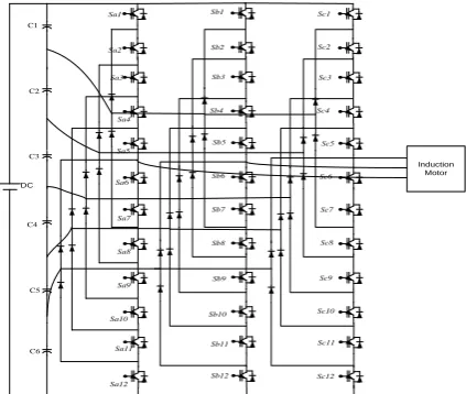
Diode Clamped Multilevel Inverter (DCMLI) topology was the first multilevel inverter (MLI) design proposed by Babaei et al. [5]. DCMLI is an attractive high-voltage multilevel inverter because of its robustness [8]. The Diode Clamped Multilevel Inverter (DCMLI) uses a single dc bus, which is further divided into a number of voltage levels using string seriesof capacitors. Each active switching device is only required for blocking a voltage level of Vdc/(m-1) -where m is the number of levels, but the clamping diodes must have different voltage ratings to block the reverse voltage [3-5]. The number of diodes essential for each phase will be (m-1) *(m-2). This number indicates a quadratic increase in m. When the number of levels goes on increasing, the number of diodes increases making the system impractical to implement.
The reverse recovery of the clamping diodes is the major problem, when we design the inverter for high-voltage and high-power by applying PWM technique.
Figure 1 shows the model for 7-level diode clamped inverter.
3. MULTI CARRIER SPWM TECHNIQUES
Modulation techniques for multilevel inverters are based on carrier arrangements. The carriers shifted horizontally is Phase Shifted Carrier PWM (PSCPWM). Generally, this technique is preferred for the CMLI, the implementation is easy and it distributes power evenly among all the cells [9]. This technique results in the termination of all carrier and associated sideband harmonics up to 2Nth carrier group, where N is the number of H-bridges in each phase [10, 11]. To implement easily on digital controller, vertical shifted carrier techniques are preferred.
Sa1 Sa2 Sb1 Sb2 Sc1 Sc2 Sa3 Sa4 Sb3 Sb4 Sc3 Sc4 Sb5 Sb6 Sc5 Sc6 Sb7 Sb8 Sc7 Sc8 Sb9 Sb10 Sc9 Sc10 Sa5 Sa6 Sa7 Sa8 Sa9 Sa10 Sa11 Sa12 Sb11 Sb12 C1 C2 C3 C4 C5 Sc11 Sc12 C6 DC Induction Motor
Figure 1. 7-level Diode Clamped Multilevel Inverter
This scheme consists of three different techniques: 1. All carrier signals are in Phase (Phase
Disposition-PD).
2. Half of the carrier signals above are in same phase and half below carriers are in same phase but the phase difference between these two half’s is 1800 (Phase Opposition Disposition- POD).
3. All carriers are alternatively in opposition (Alternate Phase Opposition Disposition – APOD). The switching frequency will be high, to reduce the undesired side effects of irregular power flow at switching and to ease lower harmonics in the output voltage.
The fundamental reference waveform of individual phase with the addition of common mode third-harmonic term increases the modulation index of a three phase inverter. As the common voltages neutralize among the phase legs, the third harmonic component has no influence on the line to line fundamental output voltage, but it reduces the maximum value of each phase leg voltage. Therefore, the modulation index can be amplified without entering into over modulation.
With the magnitude 1/6 of third harmonic injected waveform and 1.15 of fundamental waveform the reference waveform magnitude is increased. The reference voltages for Third Harmonic Injected Phase Shifted Carrier (THIPSC) technique are:
( ) 1.15sin( ) (1/ 6)sin(3 ) a
V t wt wt (1)
( ) 1.15sin( 2* / 3) (1/ 6) sin(3 ) b
V t wt pi wt (2)
( ) 1.15sin( 4* / 3) (1/ 6) sin(3 ) c
V t wt pi wt (3)
4. MODIFIED CARRIER-BASED SVPWM
Before comparing with carrier waves, sinusoidal references are included with proper offset voltage to reach the performance of SVPWM in carrier based PWM technique [14]. The calculation of offset voltage depends on modulus function which depends on the DC link voltage, number of levels and the phase voltage magnitudes.
Another modulation technique is provided in which sinusoidal reference phase voltages are included with common mode voltage of appropriate magnitude all through the interval [15, 16]. Addition of common mode voltage will not give the same performance of SVPWM, because middle inverter vectors will not be centered in a sampling interval [17]. Another modulation technique is provided in [18, 19], where a fixed common mode voltage is included with the reference phase voltage all through the modulation range.
To determine correct offset times for centering the time durations of middle inverter vectors in a sampling interval one simplified method is presented. Procedure is given in [20, 21] for finding the maximum probable peak amplitude of the fundamental phase voltage in the linear modulation. The following equations are used to calculate offset time Toffset.
* a s a dc V T T V (4) * b s b dc V T T V (5) * c s c dc V T T V (6)
where, Ta, Tb and Tc are the time periods of imaginary switching, proportional to the instantaneous values of the reference phase voltages Va, Vb and Vc and Ts is the sampling time period.
0 min [ ] 2 offset T
T T (7)
0 [ s effect]
T T T (8)
max min
effect
T T T (9)
Tmax = Maximum magnitude of the three reference phase voltages, in a sampling interval.
Tmin = Minimum magnitude of the three reference phase voltages, in a sampling interval.
The inverter switching vectors are centered in a sampling interval by the addition of offset voltage to the reference phase voltages that equate the performance of SPWM technique with the SVPWM technique.
This proposed SVPWM signal generation does not involve look up table, sector identification, angle
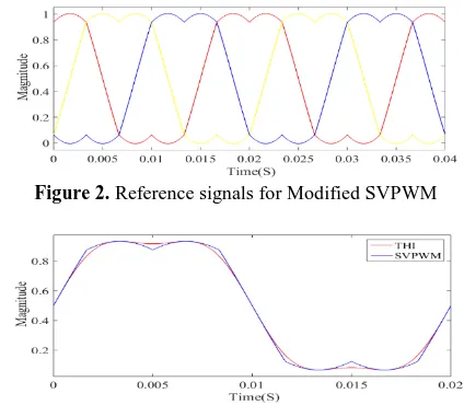
information and voltage space vector amplitude measurement for switching vector determination required in the conventional multilevel SVPWM technique. This scheme is more effective when compared with conventional multilevel SVPWM technique. Figure 2 shows the generated there-phase reference waveforms by the modified SVPWM technique. These reference waveforms are compared with triangular and trapezoidal triangular carriers to generate gate pulses for the switching devices. Figure 3 shows the comparison between the reference waveforms generated by modified SVPWM and third harmonic injected techniques.
Figure 4 shows the comparison of reference waveform generated by modified SVPWM technique with level shifted triangular carrier waveforms to generate gate pulses for the switching devices. Figure 5 shows the gate pulses generated by PDSVPWM technique. It is observed that the active switching pulses are centered in a sampling interval. Then this equates the performance with conventional SVPWM technique. This modified SVPWM can be applied to any number of levels, no limitations for this method. If the numbers of levels are increased correspondingly the numbers of carrier waves required are increased.
5. SIMULATION RESULTS AND DISCUSSION
Simulations are carried out using Matlab/Simulink environment for the 7-level DCMLI by implementing SPWM, THIPWM and Modified SVPWM techniques. A 3-phase induction motor is considered as load for this scheme. Single DC voltage source of 400 V is connected to the DCMLI. The frequency of carrier wave in all the techniques is 1350 Hz. The THD is measured for line-to-line voltage for all the PWM techniques.
Figure 2. Reference signals for Modified SVPWM
(a) PDSVPWM
(b) PODSVPWM
(c) APODSVPWM
(d) PDSVPWM- Trapezoidal
Figure 4. Different Modified SVPWM techniques
Figure 5. Gate pulses for modified SVPWM technique
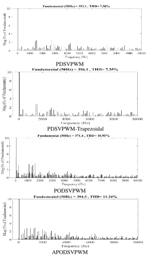
Figures 6(a), (c), (d) show the harmonic analysis of DCMLI for different SPWM techniques with triangular as carrier and Figure 6(b) shows harmonic analysis with trapezoidal triangular as carrier for the PDSPWM technique. The fundamental component in all the techniques is the same and is around 342 V. The number of levels in the output phase voltage is seven and in line voltage is 13. The PDSPWM with trapezoidal triangular carrier gives 10.12% of harmonics, which is better with respect to other SPWM techniques. The PODSPWM and APODSPWM techniques give almost similar performances in terms of %THD and magnitude of fundamental component.
Figures 7(a), (c), (d) shows the harmonic analysis of DCMLI for different THI techniques with triangular as carrier and Figure 7(b) shows the harmonic analysis with trapezoidal triangular as carrier for the PDTHI technique. The fundamental component in all the techniques is the same but the PDTHI with trapezoidal triangular technique produces more. The utilization of
DC link is almost 3% more in the THI technique with triangular carrier and is 6% more with trapezoidal triangular carrier wave with respect to the SPWM techniques. The PDTHI with triangular carrier gives 8.57% of THD, which is better harmonic performance to other THI techniques.
(a) PDSPWM
(b) PDSPWM-Trapezoidal
(c) PODSPWM
(d) APODSPWM
Figure 6. Harmonic analysis of DCMLI for different SPWM techniques
PDTHI
PDTHI- Trapezoidal
PODTHI
APODTHI
Figure 7. Harmonic analysis of DCMLI for different THIPWM techniques
PDSVPWM
PDSVPWM-Trapezoidal
PODSVPWM
APODSVPWM
The PDSVPWM with trapezoidal triangular carrier gives 7.35% of the THD, which is better harmonic performance to other SVPWM techniques.
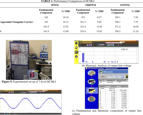
The Table 1 gives the performance comparison of a 7-level Diode clamped inverter for different Sinusoidal, Third Harmonic injected and Space vector PWM techniques. The performance of the Diode clamped inverter for POD and APOD are almost similar for all the three modulation techniques in terms of %THD. The utilization of DC link voltage is almost 15% more in SVPWM technique and 3% more in THIPWM with respect to the SPWM technique for triangular carrier wave and it is further more for trapezoidal triangular carrier wave. The percent of THD is approximately the same for both carrier waves.
The PDTHI and PODTHI give superior harmonic performance with respect to corresponding SPWM techniques. All SVPWM techniques give better harmonic performance corresponding to the other two techniques. The PDS VPWM technique with trapezoidal
triangular as carrier produces better harmonics values of 7.35% with respect to all other PWM techniques.
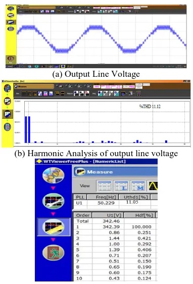
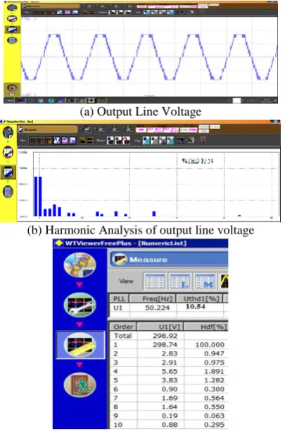
6. EXPERIMENTAL RESULTS
To validate the proposed PWM techniques, a seven-level three-phase Diode-Clamped Inverter is designed. Figure 9 shows the experimental set up for this seven-level DCMLI. The necessary experimental parameters for DCMLI are as follows; each dc link capacitance-2200 μF, output frequency- 50 Hz, the frequency of carrier wave- 1 kHz, total dc link voltage- 400 V and the rating of each IGBT- 1200V/75A. The PDSPWM,
PDTHIPWM, PDSVPWM, PODSVPWM and
APODSVPWM techniques are implemented.
The experimental results of DCMLI for
PDSVPWM, PODSVPWM and APODSVPWM
techniques are shown in Figures 10, 11 and 12.
TABLE 1. Performance Comparison of DCMLI
SPWM THIPWM SVPWM
Fundamental
Component % THD
Fundamental
Component % THD
Fundamental
Component % THD
PD 342 10.18 353 8.57 393.1 7.58
PD (Trapezoidal Triangular Carrier) 343 10.12 361.3 9.04 396.1 7.35
POD 341.9 13.92 353.4 15.85 371.4 10.95
APOD 341.9 13.60 353.4 15.62 394.5 11.24
Figure 9. Experimental set up of 7-level DCMLI
(a) Output Line Voltage
(b) Harmonic Analysis of output line voltage
(c) Fundamental and Harmonic components of output line voltage
(a) Output Line Voltage
(b) Harmonic Analysis of output line voltage
(c) Fundamental and Harmonic components of output line voltage
Figure 11. Performance analysis of DCMLI for PODSVPWM
(a) Output Line Voltage
(b) Harmonic Analysis of output line voltage
(c) Fundamental and Harmonic components of output line voltage
Figure 12. Performance analysis of DCMLI for APODSVPWM
After validating the results, the PDSVPWM technique shows its superiority among all other SVPWM techniques with THD of 7.98 and the line voltage is
exactly having 13-levels. The PODSVPWM and
APODSVPWM techniques similar performances in terms %THD and fundamental component of output voltage. The dc link utilization is almost 15% more with respect to SPWM technique. These experimental performances are approximately the same as simulation performances.
The experimental results of DCMLI for PDSPWM, and PDTHIPWM techniques are shown in Figures 13 and 14 respectively. The PDSPWM technique gives better THD% of 9.92 with respect to PDTHIPWM technique, but PDTHIPWM gives high fundamental component of output voltage.
It is observed from all the experimental results, the PDSVPWM technique performance is good in terms of THD% and utilization of dc link voltage. The experimental performance with all the techniques is approximately the same as simulation performances.
(a) Output Line Voltage
(b) Harmonic Analysis of output line voltage
(c) Fundamental and Harmonic components of output line voltage
(a) Output Line Voltage
(b) Harmonic Analysis of output line voltage
(c) Fundamental and Harmonic components of output line voltage
Figure 14. Performance analysis of DCMLI for PDTHIPWM
6. CONCLUSION
In this paper, modified SVPWM techniques such as Phase Disposition (PD), Phase Opposition Disposition (POD), and Alternate Phase Opposition Disposition (APOD) have been implemented along with SPWM and THIPWM techniques for 7-level DCMLI. These results are analysed and are compared with other techniques. To validate these simulation results, these PWM techniques implemented experimentally on 7-level DCMLI with only triangular carrier wave. It is observed that from the simulation results, PDSVPWM technique with Trapezoidal Triangular carrier gives better THD percent of 7.35, which is a better performance with respect to other techniques. The utilization of DC link voltage is almost 15% more in the SVPWM technique with triangular carrier and is around 16% more with trapezoidal triangular carrier wave with respect to the SPWM techniques. The performance of the Diode clamped inverters for POD and APOD are almost similar for all the three modulation techniques in terms of THD percent. It is observed from the experimental results, the PDSVPWM technique performance is better in terms of THD percent and utilization of dc link
voltage. All the experimental results give similar performances with respect to simulation results.
7. ACKNOWLEDGMENT
We thank the DST, New Delhi, for providing support to carryout research on diode clamped multilevel inverter under major research project.
8. REFERENCES
1. Masaoud, A., Ping, H.W., Mekhilef, S. and Belkamel, H.O., "A new five-level single-phase inverter employing a space vector current control", Electric Power Components and Systems, Vol. 42, No. 11, (2014), 1121-1130.
2. Rodriguez, J., Lai, J.-S. and Peng, F.Z., "Multilevel inverters: A survey of topologies, controls, and applications", IEEE Transactions on Industrial Electronics, Vol. 49, No. 4, (2002), 724-738.
3. Belkamel, H., Mekhilef, S., Masaoud, A. and Naeim, M.A., "Novel three-phase asymmetrical cascaded multilevel voltage source inverter", IET Power Electronics, Vol. 6, No. 8, (2013), 1696-1706.
4. Mohamad, A.S., Mariun, N., Sulaiman, N. and Radzi, M.A.M., "A new cascaded multilevel inverter topology with minimum number of conducting switches", in Innovative Smart Grid Technologies-Asia (ISGT Asia), IEEE, (2014), 164-169. 5. Ebrahimi, J., Babaei, E. and Gharehpetian, G.B., "A new
multilevel converter topology with reduced number of power electronic components", IEEE Transactions on Industrial Electronics, Vol. 59, No. 2, (2012), 655-667.
6. Lai, J.-S. and Peng, F.Z., "Multilevel converters-a new breed of power converters", IEEE Transactions on Industry Applications, Vol. 32, No. 3, (1996), 509-517.
7. Gayathri, M.N. and Ganimozhi, T., "New hybrid cascaded multilevel inverter", International Journal of Engineering-Transactions B: Applications, Vol. 26, No. 11, (2013), 1377-1385.
8. Masaoud, A., Ping, H.W., Mekhilef, S. and Taallah, A., "Novel configuration for multilevel dc-link three-phase five-level inverter", IET Power Electronics, Vol. 7, No. 12, (2014), 3052-3061.
9. Rodriguez, J., Bernet, S., Steimer, P.K. and Lizama, I.E., "A survey on neutral-point-clamped inverters", IEEE Transactions on Industrial Electronics, Vol. 57, No. 7, (2010), 2219-2230. 10. Raj, P.H., Maswood, A.I., Ooi, G.H. and Lim, Z., "Voltage
balancing technique in a space vector modulated 5-level multiple-pole multilevel diode clamped inverter", IET Power Electronics, Vol. 8, No. 7, (2015), 1263-1272.
11. Salam, Z., "A fast and efficient on-line harmonics elimination pulse width modulation for voltage source inverter using polynomials curve fittings", International Journal of Engineering Transaction B: Applications, Vol. 23, No. 1, (2010), 53-68.
12. Mekhilef, S. and Kadir, M.N.A., "Voltage control of three-stage hybrid multilevel inverter using vector transformation", IEEE Transactions on Power Electronics, Vol. 25, No. 10, (2010), 2599-2606.
space vector modulation", IET Power Electronics, Vol. 7, No. 5, (2014), 1256-1265.
14. Shukla, A., Ghosh, A. and Joshi, A., "Control of dc capacitor voltages in diode-clamped multilevel inverter using bidirectional buck–boost choppers", IET Power Electronics, Vol. 5, No. 9, (2012), 1723-1732.
15. Grigoletto, F.B. and Pinheiro, H., "Generalised pulse width modulation approach for dc capacitor voltage balancing in diode-clamped multilevel converters", IET Power Electronics, Vol. 4, No. 1, (2011), 89-100.
16. McGrath, B.P. and Holmes, D.G., "Multicarrier pwm strategies for multilevel inverters", IEEE Transactions on Industrial Electronics, Vol. 49, No. 4, (2002), 858-867.
17. Naderi, R. and Rahmati, A., "Phase-shifted carrier pwm technique for general cascaded inverters", IEEE Transactions on Power Electronics, Vol. 23, No. 3, (2008), 1257-1269.
18. Lee, D.-C. and Lee, G.-M., "A novel overmodulation technique for space-vector pwm inverters", IEEE Transactions on Power Electronics, Vol. 13, No. 6, (1998), 1144-1151.
19. Yao, W., Hu, H. and Lu, Z., "Comparisons of space-vector modulation and carrier-based modulation of multilevel inverter",
IEEE Transactions on Power Electronics, Vol. 23, No. 1, (2008), 45-51.
20. Kang, W., Lee, Y.-H., Suh, B.-S., Choi, C.-H. and Hyun, D.-S., "An improved carrier-based svpwm method using leg voltage redundancies in generalized cascaded multilevel inverter topology", IEEE Transactions on Power Electronics, Vol. 18, No. 1, (2003), 180-187.
21. Chintala, L.R., Peddapelli, S.K. and Malaji, S., "Improvement in performance of cascaded multilevel inverter using triangular and trapezoidal triangular multi carrier svpwm", Advances in Electrical and Electronic Engineering, Vol. 14, No. 5, (2016), 562-570.
Design and Performance Analysis of 7-Level Diode Clamped Multilevel Inverter
Using Modified Space Vector Pulse Width Modulation Techniques
C. Lokeshwar Reddya, P. Satish Kumarb, M. Sushamac
a Department Electrical and Electronics Engineering, CVR College of Engineering, Hyderabad, Telangana, India
b Department of Electrical Engineering, University College of Engineering, Osmania University, Hyderabad, Telangana, India c Department Electrical and Electronics Engineering, College of Engineering, JNT University, Hyderabad, Telangana, India
P A P E R I N F O
Paper history: Received 03 March 2016
Received in revised form 05 April 2017 Accepted 07 July 2017
Keywords:
Diode Clamped Multilevel Inverter Phase Disposition Space Vector Pulse Width Modulation
Phase Opposition Disposition Space Vector Pulse Width Modulation
Alternate Phase Opposition Disposition Space Vector Pulse Width Modulation
ديكچ ه
کی هلاقم نیا رد رگنوراو
(Inverter) یحطس دنچ
اب یدویاد راهم و
حطس تفه (DCMLT) شور هس اب
PWM لماح و
(Carrier) یسونیس سلاپ یانهپ نویسلاودم نیا رد .تسا هدش یزاس هیبش فلتخم یاه
(SPWM) ،لماح یانبم رب
موس کینومراه قیرزت اب سلاپ یانهپ نویسلاودم (THIPWM)
رادرب سلاپ یانهپ نویسلاودم و لماح یانبم رب ییاضف
هدش حلاصا (SVPWM)
.تسا هتفر راک هب نویسلاودم یاه یژتارتسا ناونع هب یژتارتسا نیا
اه تروص شور لماش
،زاف یدنب (PD) فلاخم زاف یدنب تروص شور ، (POD)
فلاخم زاف یدنب تروص زا یرگید شور و ، (APOD)
.دشاب یم
یم هسیاقم عجرم لانگیس اب یا هفنذوذ یلیطتسم لماح و یثلثم لماح یاه لانگیس ،نویسلاودم یاه یژتارتسا نیا مامت رد
هدش هئارا تایئزج اب جیاتن لیلحت .دندرگ یم دیلوت لرتنک یاه سلاپ سپس و دنوش یاه هفلوم رظن زا یشیامزآ جیاتن اب و
دص رد و یجورخ ژاتلو یداینب THD
.تسا هدش هسیاقم