ISSN : 2581-7175
©IJSRED: All Rights are Reserved
Page 440
Low-Power and High Speed Full Adder Using
Optimized XOR and XNOR GATE Structures
Shobika.C
[1],Mr.G.Prabakaran- Assistant Professor
[2]Department of Electronics and Communication Engineering, NandhaEngineering College, Erode
[1]
[email protected], [2][email protected]
Abstract—
In this paper, novel circuits for XOR/XNOR and synchronous XOR–XNOR capacities are proposed. The proposed circuits are profoundly enhanced as far as the power utilization what's more, delay, which are because of low yield capacitance and low short out power dissemination. We likewise propose six new mixture 1-piece full-viper (FA) circuits dependent on the novel full-swing XOR–XNOR or XOR/XNOR entryways. Every one of the proposed circuits has its own benefits as far as speed, control utilization, power delay item (PDP), driving capacity, etc. To research the exhibition of the proposed structures, broad HSPICE and Rhythm Virtuoso reenactments are performed. The reproduction results, in view of the 65-nm CMOS process innovation model, show that the proposed plans have unrivaled speed and power against other FA structures. Another transistor estimating technique is introduced to advance the PDP of the circuits. In the proposed strategy, the numerical calculation molecule swarm advancement calculation is utilized to accomplish the ideal incentive for ideal PDP with less emphases. The proposed circuits are researched in terms of varieties of the inventory and edge voltages, yield capacitance, input commotion insusceptibility, and the size of transistors.
Index Terms—Full Adder (FA), clamor, molecule swarm streamlining (PSO), transistor measuring technique, XOR–XNOR.
I. INTRODUCTION
TODAY, pervasive electronic frameworks are an indistinguishable some portion of regular daily existence. Advanced circuits, e.g., chip, advanced specialized gadgets, and computerized signal processors, contain a huge piece of electronic frameworks. As the size of reconciliation builds, the ease of use of circuits is confined by the enlarging measures of intensity [1] and region utilization. Thusly, with the developing notoriety and interest for the battery-worked convenient gadgets, for example, cell phones, tablets, and PCs, the creators attempt to lessen control utilization and territory of such frameworks while saving their speed. Enhancing the W/L proportion of transistors is one way to deal with decline the power-defer item (PDP) of the circuit while forestalling the issues came about because of lessening the stockpile voltage [2]. The effectiveness of numerous computerized applications applies to the exhibition of the number-crunching circuits, for example, adders, multipliers, and dividers. Because of the key job of expansion in all the math tasks, numerous endeavors have been made to them of investigate proficient snake structures,e.g., convey select, convey skip, contingent whole, and the tasks of the gates. Full adders are the important role in the circuits. convey look-ahead adderstasks,numerous endeavors have been made to investigate proficient snake structures of investigate proficient snake structures,e.g., convey select, convey skip, contingent whole, and
convey look-ahead adderstasks, numerous endeavors have been made to investigate proficient snake structures, e.g., convey select, convey skip, contingent whole, and convey look-ahead adders. Full snake (FA) as the major square of these structures is at the focal point of consideration [3]–[5]. In view of the yield voltage level, Full adder of circuits can be isolated into full-swing and nonfull-swing classes. Standard CMOS [2], [6], reciprocal pass-transistor rationale (CPL) [7], [8], transmission door (TG) [9]–[11], transmission work [2], [10], [12], 14T (14 transistors) [7], [13], 16T [10], [12], [14], [15], and cross breed pass rationale with static CMOS yield drive full snake (HPSC) [3], [12], [16]–[20] FAs are the most significant full-swing families. Nonfull-full-swing classification involves 10T [4], 9T [21], and 8T [22]. In this paper, we assess a few circuits for the XOR or XNOR (XOR/XNOR) and synchronous XOR and XNOR (XOR– XNOR) doors and offer new circuits for every one of them. Additionally, we attempt to evacuate the issues existing in the explored circuits. A short time later, with these new XOR/XNOR and XOR–XNOR circuits, we propose six new FA structures. The remainder of this paper is sorted out as pursues. In Section II, the circuits for XOR/XNOR and synchronous XOR–XNOR are checked on. In Section III, novel XOR/XNOR and XOR–XNOR circuits are proposed and the reenactment aftereffects of these structures are exhibited. Moreover, in view of the presented XOR/XNOR and XOR–XNOR doors, six new FA circuits are proposed and points of interest and burdens of them are researched. In Section IV, the
ISSN : 2581-7175
©IJSRED: All Rights are Reserved
Page 441
transistor measuring strategies are first researched, and afterward by
giving a suitable technique to transistor measuring, the circuits are mimicked for power, delay, furthermore, PDP parameters. The recreation results are broke down and looked at in Section V. Segment VI closes this paper.
II. Audit OF XOR AND XNOR GATES
A.XOR–XNOR Circuits
Crossover FAs are made of two modules, including 2-input XOR/XNOR (or synchronous XOR–XNOR) entryway and 2-to-1
multiplexer (2-1-MUX) door [3]. The XOR/XNOR entryway is the
real purchaser of intensity in the FA cell. Consequently, the power utilization of the FA cell can be diminished by ideal structuring of the XOR/XNOR entryway. The XOR/XNOR door has additionally numerous applications in computerized circuits structure. Numerous circuits have been proposed to execute XOR/XNORdoor[11], [12], [16], [24], which a couple of instances of the full swing structure.
Figure .1 (a) and (b) Full-swing XOR/XNOR and (c)–(g) XOR–XNOR circuits. (a)[6]. (b) [11]. (c) [10]. (d) [3]. (e) [7], [12]. (f) [1]. (g) [9].
ofmost the full-swing XOR/XNOR door circuit [16] structuredproficient ones are appeared in Fig. 1. Fig. 1(a) demonstratestwofold pass-transistor rationale (DPL) style.This structure has eight transistors. The primary issue of this circuit is utilizing two high power utilization NOT entryways on the of the fact that the entryways must drive the yield capacitance.In this way, the size of the transistors in the NOT entryways ought to be expanded to acquire lower basic way delay. Moreover, it causes the making of a middle hub with a huge capacitance. Obviously, this implies the NOT entryways drives the yield of circuit through, for instance, pass transistor or TG. In this manner, the short out power and, accordingly, the complete power dissemination of this circuit are generally increased. Moreover, in the ideal PDP circumstance, the basic way defer will likewise be expanded marginally. Fig. 1(b) demonstrates another case of the full-swing XOR/XNOR entryway [11], each made of six transistors. This circuit depends on the PTL rationale style, whose deferral and power utilization are superior to anything the circuit delineated in Fig. 1(a). The main issue of this structure is utilizing a NOT entryways on the basic way of the circuit. The XOR circuit of Fig. 1(b) has the lower delay than its XNOR circuit, on the grounds that the basic way of XOR circuit is contained a NOT doors with an NMOS transistor (N3). Be that as it may, the basic way of XNOR circuit is contained a NOT doors and a PMOS Transistor (P5) (PMOS transistor is more slow than NMOS transistor). In this way, to improve the XNOR circuit speed, the size of PMOS transistor (P5) and NOT entryways ought to be expanded.
B. Synchronous XOR–XNOR Circuits
ISSN : 2581-7175
©IJSRED: All Rights are Reserved
Page 442
XNOR yield. At the point when the sources of info change to AB = 00, all transistors will be killed with the exception of transistors N2 (through the info A)what's more, P2 (through the XNOR yield, which has not changed presently). Accordingly, the short out current will go from the transistors P2 and N2. On the off chance that the measure of current beingsourced from the transistor P2 is bigger than that of current being sunk from the transistor N2, the short out current will keep on being drawn from VDD and will never switch XOR what's more, XNOR yield. This circumstance likewise happens when the info is changed from AB = 11 to AB = 10 and effects the best possible working of the circuit. To grantee the best possible activity of this circuit, the ON-state opposition of transistors P2 and P3 ought not be littler than that of transistors N2 and N5 (RP2 > RN2, RP3 > RN5), separately. Besides, this structure is extremely delicate to process variety; if the size of transistors is changed, the circuit may not work appropriately. In [7] and [13], full-swing XOR– XNOR entryway with as it were six transistors is proposed [shown in Fig. 1(e)]. The two reciprocal criticism transistors (N3 and P3) reestablish the powerless rationale in the yield hubs (XOR and XNOR) when the data sources equivalent to AB = 00, 11. Nonetheless, this circuit endures from the high most pessimistic scenario delay, since when the data sources change from AB = 01, 10 to AB = 11, 00, the yields arrive at its last voltage esteem in two stages. To explain the issue, at the point when the information sources equivalent to AB = 10, rationale "1" and rationale "0" are gone through the N2 (NOR yield) and P2 (XNOR yield) transistors, individually. By changing the information mode to Abdominal muscle = 11, the transistors P1 and P2 are killed (XOR hub is at first high impedance) and frail rationale "1" (VDD−Vthn) is gone through the transistors N1 and N2 to the XNOR yield. The frail rationale "1" on the XNOR turns ON the criticism N3 so that the XOR yield isdismantled down to powerless rationale "0," which this feeble rationale "0" turns ON the criticism P3. In the long run, positive input is made and the XNOR and XOR yields will have solid rationale "1" and rationale "0," individually. This slow reaction issue is more awful in the low-voltage activityand furthermore builds the short out current [when one of the yields (XOR or XNOR) is high impedance and circuit criticism has not yet acted totally, the short out current is going through the circuit]. Additionally, if the size of transistors in this circuit isn't appropriately chosen, the circuit may not be accurately worked. Consequently, this structure is touchy to process–voltage–temperature (PVT) varieties. Chang et al. [18] have proposed another structure of the concurrent XOR–XNOR entryway [shown in Fig. 1(f)] by improving the six-transistor XOR–XNOR circuit of Fig. 1(e). In the circuit of Fig. 1(f), to take care of the moderate reaction issue and work in low voltage supplies two nMOS transistors (for Stomach muscle = 11) and two pMOS. The favorable circumstances of this structure are great driving ability, full swing yield, and strength against transistor estimating and supply voltage scaling. The primary issue of this circuit is the structure of input that forces extra parasitic capacitance to the XOR and XNOR yield hubs.
Figure. 2 (a) Nonfull-swing XOR/XNOR door [24]. (b) Proposed full-swing XOR/XNOR door. (c) RC model of proposed XOR for AB =10. (d) RC model
of proposed XOR for AB = 11. (e) Proposed XOR–XNOR door.
In this way, the postponement and power utilization essentially increment. Fig. 1(g) [23] demonstrates another circuit for improving the structure of Fig. 1(e). In this structure, a NOT entryway is utilized to improve the circuit speed. This circuit has a superior speed than Fig. 1(e), on the grounds that in Fig. 1(g), the transistors N5 and P5 have the way from GND or VDD to the yield hubs in two conditions of information sources (AB = X1 for N5 and AB = X0 for P5). Be that as it may, in Fig. 1(e), the transistors N4 and P5 have a similar way for just one condition of information sources (AB = 11 for N4 and AB = 00 for P5). Additionally, with the option of a NOT door, a transitional hub with a huge capacitance will be made that will increment the power utilization of the circuit. In this manner, Fig. 1(g) has more power utilization than Fig. 1(e). Mix of two XOR and XNOR circuits of Fig. 1(a) and (b) will bring about two synchronous XOR–XNOR doors. These new structures will have all points of interest and drawbacks of their XOR/XNOR circuits.
III. PROPOSED CIRCUITS
A.Proposed XOR–XNOR Circuit
ISSN : 2581-7175
©IJSRED: All Rights are Reserved
Page 443
is likewise associated with the NOT entryways, to the transistor with littler info capacitance. By doing this, the info capacitances are progressively balanced, furthermore, in this way, the postponement and power utilization of the circuit will be decreased. To explain which transistor (N2 or N3) has bigger input capacitance, let us consider the condition that the information sources change from AB = 10 to AB = 00. In this condition, as the RC model of XOR is appeared in Fig. 2(c) and (d), the transistor N2 is driving just the capacitance of hub X from GND to VDD − Vthn [Fig. 2(c)], so it won't require lower RN2. Be that as it may, at the point when thesources of info change from AB = 10 to AB = 11, agreeing to Fig. 2(d), we have
kN2 = WN2 /Wmin , kN3 = WN3 /Wmin , . . . , kP3 = WP3 /Wmin
RN2 = Rmin/kN2 , RN3 = Rmin/ kN3 , a = kN4 + kP2 + kP3
CX = Cdmin × kN2 + Cdmin × kN3 = Cdmin (kN2 + kN3)
Cout = CdN4 + CdP2 + CdP3 + Cdmin × kN2
Cout = a × Cdmin + Cdmin × kN2 = Cdmin (a + kN2) (1)
whereWmin is the base transistor width, Rmin is the ON-state obstruction for the nMOS transistor with Wmin,
Cdmin is the dispersion capacitance of the transistor, and an is the aggregate size of the transistors P2, P3, and N4.
The Elmore delay [25] (TdAB=10→11 ) of Fig. 2(c) and (d) is equivalent to TdAB=10→11 = Cout(Rmin/kN2 + Rmin/ kN3 )+ CX (Rmin/ kN3)= CdminRmin[a(1/ kN2 + 1 /kN3) + 2( 1 + kN2/ kN3 )](2)
presently, the normal unique power dissemination (for the condition that the data sources change from AB = 10 to AB = 11) can be composed as [2] PAB=10→11 = CtotalVDD2 = (Cdmin (kN2 + kN3) +Cdmin (a + kN2) + kN3Cgmin + kP2Cdmin +kP3Cgmin + kN4Cdmin )VDD 2 (3)where Cgmin is the entryway capacitance of the transistor, and Ctotal is all capacitances that are exchanged. Byaccepting Cdmin ≈ Cgmin = C and a = 3 (the size of transistors P2, P3, and N4 equivalent to the Wmin). The equations are given by,
PAB=10→11 = ((kN2 + kN3)C + (3 + kN2)C +kN3C + 3C)VDD 2 = CVDD 2(2kN2 + 2kN3 + 6). (4)
At last, by having the estimation of deferral and power dissemination, the PDP of the circuit can be gotten. For a superior examination, the standardized PDP (PDPn) is considered
PDPn = TdAB=10→11 × PAB=10→11 /CRmin × CVDD 2
= [3( 1/ kN2 + 1/ kN3 )+2( 1+kN2 /kN3)] (2kN2+2kN3+6).(5)
Fig. 3 demonstrates the estimation of standardized PDP with a = 3for 1 ≤ kN2, kN3 ≤ 4. Fig. 3 additionally demonstrates that, in the ideal condition, the estimation of kN3 is greater than that of kN2. In this manner, the W/L proportion of the transistor N3 is bigger than that of the transistor N2.
In this manner, the information capacitance of transistor N3 is higher than that of transistor N2 and, to get the ideal circuit, it is smarter to interface input A to the transistor N2. The benefits of the proposed XOR/XNOR circuits are full-swing yield, great driving ability, littler number of interconnecting wires, and direct circuit format. Fig. 4(a) and (b) demonstrates the circuit design of the proposed XOR and XNOR entryways, separately, intended for least power utilization [26].
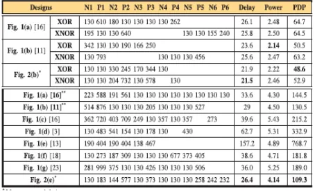
TABLE I
RECREATION RESULTS (OPTIMUM SIZE OF TRANSISTORS IN nm, POWER IN e-6W, DELAY IN ps, AND PDP IN aJ) FOR XOR/XNOR AND Concurrent XOR–XNOR CIRCUITS IN 65-nm TECHNOLOGYWITH 1.2-V POWER SUPPLY VOLTAGE AT 1
GHz
B. Proposed XOR–XNOR Circuit
ISSN : 2581-7175
©IJSRED: All Rights are Reserved
Page 444
ability, full-swing yield, just asstrength against transistor estimating and supply voltage scaling. The proposed XOR/XNOR and synchronous XOR–XNOR structures were contrasted and all the previously mentioned structures (Fig. 1). The reproduction results at TSMC 65-nm innovation what's more, 1.2-V power supply voltage (VDD) are appeared in Table I. The information example is utilized as all conceivable information mixes have been incorporated [Fig. 5(a)]. The most extreme recurrence for the information sources was 1 GHz and 4× unit-size inverter (FO4) was associated with the yield (as a heap). The size of transistors has been chosen for ideal PDP by utilizing the proposed transistor estimating strategy, which the proposed method will be portrayed in Section VI. The ideal size of transistors for each XOR/XNOR and XOR–XNOR circuits are communicated in Table I. In the yield rise and fall change, the postponement is determined from half of the info voltage level to half of the yield voltage level. The PDP will be determined by increasing the most pessimistic scenario delay by the normal power utilization of the principle circuit. The outcomes show that the exhibition of the proposed XOR/XNOR and concurrent XOR– XNOR structures is betterthan that of the analyzed structures. The proposed XOR and XNOR circuits [Fig. 2(b)] have the least PDP and deferral, separately, contrasted and other XOR/XNOR circuits. Moreover, the deferral of these two proposed circuits is near one another that avoids the formation of glitch on the following stage. The delay, control utilization, and PDP of the XOR and XNOR circuits of Fig. 1(a) are practically equivalent, due to having the same structures. As referenced before and as indicated by the acquired outcomes, the XOR circuit of Fig. 1(b) has a superior execution than its XNOR circuit. The proposed circuit for synchronous XOR–XNOR has better effectiveness in each of the three determined parameters (delay, control dispersal, and PDP) when it is contrasted and other XOR–XNOR doors.
Figure.3 Simulation results of XOR–XNOR circuits
The proposedXOR–XNOR circuit is sparing practically 16.2%–85.8% in PDP, and it is 9%–83.2% quicker than different circuits. The circuits of Fig. 1(d) and (e) have the extremely high deferral because of its yield input (which have the moderate reaction issue). As anyone might imagine found in Table I, the effectiveness of Fig. 1(e) is much more terrible and its postponement is multiple times more than that of different circuits. Table I demonstrates that the structures have demonstrated a superior execution, which have the base NOT entryways on the basic way and additionally have not criticism on the yields to address the yield voltage level. To all the more likely assess the XOR–XNOR circuits, they are reproduced at various power supply voltages from 0.6 to 1.5 V and likewise at various yield loads from FO1 to FO16. The aftereffects of these two reproductions are appeared in Fig. 5(b) and (c). As observed in Fig. 5(b) and (c), the proposed XOR–XNOR circuit has the best execution in the two reenactments when contrasted and different structures.
C. Proposed FAs
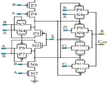
We proposed six new FA circuits for different applications which have been appeared in Figure 4 These new FAs have been utilized swith half and half rationale style, and every one of them are planned by utilizing the proposed XOR/XNOR or XOR–XNOR circuit. The notable four-transistor 2-1-MUX structure is utilized to actualize the proposed half and half FA cells. This 2-1-MUX is made with TG rationale style that has no static what's more, impede dissemination.
Figure .4Hybrid Full Adder-22T
The circuits HFA-22T and HFA-19T, have been made by applying the above plan to HFA-20T and HFA-17T, individually. It is normal that the power utilization and postponement of the HFA-22T and HFA-19T FA circuits are not as much as that of HFA-20T and HFA-17T, separately (regardless of having two more transistors), because of the less capacitance of XOR and XNOR hubs. Likewise, by including the C signal, the driving capacity of HFA-22T and HFA-19T will be superior to that of HFA-20T what's more, HFA-17T, separately.
IV. SIMULATION RESULTS
ISSN : 2581-7175
©IJSRED: All Rights are Reserved
Page 445
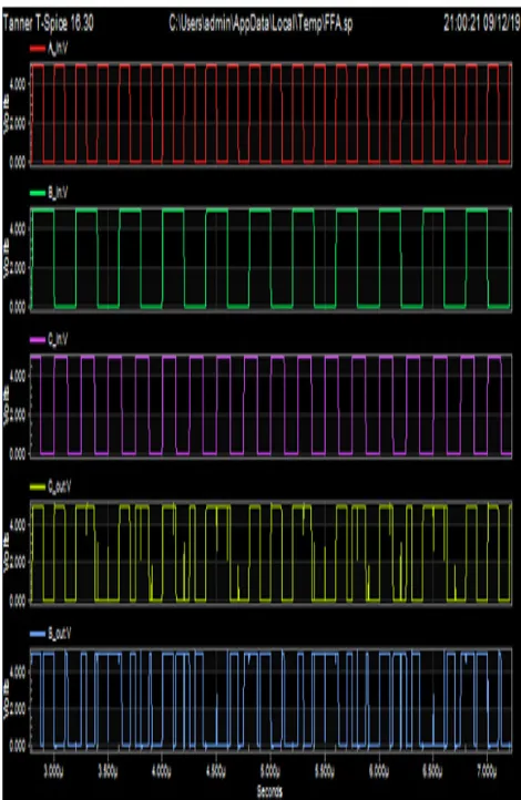
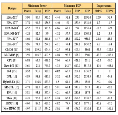
Every one of the circuits have been reproduced utilizing HSPICE in the 65-nm TSMC CMOS process innovation, and were provided with 1.2 V just as the most extreme recurrence for the information sources was 1 GHz. Fig. 8(b) and (c) demonstrates the run of the mill reenactment test seat to do the circuit parameters. There are two NOT doors on the contribution of structure appeared in Fig. 8(b) with two separate power supplies (VDD1 and VDD2 ). As can be seen in Fig. 8(b), the primary circuit and the NOT doors associated to it have a similar power supply (VDD1 ). By subtracting the power utilization of VDD1 in Fig.8(c) from the power utilization of VDD1 in Fig. 8(b), the power utilization of the primary circuit will be accomplished. The information design for the both structures of Fig. 8(b) and (c) is actually the equivalent. With this technique, the determined power utilization of the fundamental circuit will be considerably more precise and the power utilization of all input capacitance is likewise considered. Yield heap of FO4 is utilized for deferral and power dispersal estimations, which has an alternate power supply from the primary circuit. The sizes of info cradles are chosen, for example, [3] and [27]. In the yield rise and fall progress, the postponement is determined from half of the info voltage level to half of the yield voltage level. The PDP will be determined by duplicating the most pessimistic scenario delay by the normal power utilization of the fundamental circuit. Fig. 9 demonstrates the time-space recreation results (waveform) of the proposed FA. The exhibition of the FA circuits is assessed in wording of intensity utilization, most pessimistic scenario deferral, and PDP for a scope of inventory voltages (from 0.65 to 1.5 V) at 1-GHz recurrence. Moreover, their exhibitions are assessed by changing the yield burden went from FO4 to FO64 at the 1.2-V power supply voltage and 1-GHz recurrence. The most minimal control utilization of a circuit is accomplished when the width of transistors is as least as conceivable [2]. In any case, in this case, the most minimal PDP can't be ensured. Since the deferral of the circuit isn't in the ideal state and expands the PDP. To better examination, the estimations of the deferral, control utilization, what's more, PDP are displayed in Table II for a base element size (W1,2,...,n = Wmin = 4= 130 nm).
Figure.5 Time-domain simulation results (waveform) of the proposed FA.
TABLE II
SIMULATION RESULTS (POWER IN e-6W, DELAY IN ps, PDP IN aJ,AND EDP IN e-29Js) FOR FA CIRCUITS IN
ISSN : 2581-7175
©IJSRED: All Rights are Reserved
Page 446
B. Performance analysis
In this segment, the reenactments results are talked about, and likewise the presentation of the different referenced structures is thought about. In all recreations, the size of transistors is picked so that the base PDP is accomplished for the circuit. To arrive at this point, the proposed technique for transistor estimating is utilized. Table II demonstrates the reproduction aftereffects of different FA circuits. In Table II, we have detailed the normal control utilization, basic way postponement, PDP, and vitality delay item (EDP) measurements for various structures. Likewise, for better examination, the PDP and EDP upgrades of the plans contrasted and the 16T structure are given. We initially talk about the outcomes identified with the base power conditions (MPCs), which is named least power in Table II. In the predetermined information recurrence, yield load, and supply voltage, the base power utilization of a circuit is reliant on its structure and number of transistors (n), while W1,2,...,n = Wmin. The 16T circuit has the least power contrasted and different circuits. This circuit produces fullswingCout and Sum yields regardless of having the nonfull-swing XOR–XNOR signals. The CPL FA cell has the most noteworthy power, on account of having the high number of transistors, analyzed with different plans. Be that as it may, it has great speed and great driving capacity. In the MPC, the proposed HFA-22T recoveries the PDP of about 24%, 32%, 40%, 41%, 42%, and half contrasted and 16T, TFA, Mir-CMOS, TGA, New-HPSC, and DPL, individually. By looking at the acquired outcomes for the MPC and least PDP conditions (MPDPCs), the effectiveness of transistor measuring techniques, which is utilized for improving the presentation of the circuits, turns out to be so obvious. By contrasting the outcomes of MPC and MPDPC, the most extreme improvement in PDP is accomplished for the Hybrid-FA circuit which is equivalent to 33%. Additionally, the CPL FA circuit indicates 2% improvement in PDP metric that is lower than different structures. For the most part, for CPL rationale style, the size of transistors in the MPC and MPDPC is near one another [26]. In the accompanying, we talk about the reenactment results for the MPDPC. The proposed FAs have unrivaled speed, PDP,
and EDP against other FA structures. The 16T circuit expends lower control than that of other FA cells. Additionally, it shows better PDP and EDP contrasted and different circuits aside from the FAs exhibited in this paper. The proposed HFA-22T circuit has the best deferral, PDP, and EDP among FA cells. The structures of HFA-B-26T, HFA-NB-26T, CMOS, M-CMOS, CPL, HPSC, what's more, New-HPSC have cushions at their yields. The proposed HFA-NF-26T circuit spares PDP up to 35%, 31%, 39%, 32%, furthermore, 45% contrasted and CMOS, M-CMOS, CPL, HPSC, and New-HPSC, separately.
V.CONCLUSION
In this paper, we initially assessed the XOR/XNOR and XOR– XNOR circuits. The assessment uncovered that utilizing the NOT entryways on the basic way of a circuit is a disadvantage. Another burden of a circuit is to have a positive criticism on the yields of the XOR–XNOR door for repaying the yield voltage level. This criticism builds the postponement, yield capacitance, and, subsequently, vitality utilization of the circuit. At that point, we proposed new XOR/XNOR and XOR–XNOR doors that try not to have the referenced weaknesses. At long last, by utilizing the proposed XOR and XOR–XNOR doors, we offered six new FA cells for different applications. Moreover, an adjusted technique for transistor estimating in computerized circuits was proposed. The new technique uses the numerical calculation PSO calculation to choose the fitting size for transistors on a circuit and furthermore it has awesome speed, exactness, furthermore, combination. In the wake of reenacting the FA cells in various conditions, the outcomes exhibited that the proposed circuits have an excellent presentation in every mimicked condition. Recreation results demonstrate that the proposed HFA-22T cell spares PDP and EDP up to 23, 4% and 43.5%, individually, contrasted and its best partner. Additionally, this cell has better speed and vitality at all stock voltages going from 0.65 to 1.5 V when is contrasted and other FA cells. The proposed HFA-22T has prevalent speed and vitality against other FA plans at all unique procedure corners. All proposed FAs have typical affectability to PVT varieties.
REFERENCES
[1] N. S. Kim et al., “Leakage current: Moore’s law meets static power,”Computer, vol. 36, no. 12, pp. 68–75, Dec. 2003. [2] N. H. E. Weste and D. M. Harris, CMOS VLSI Design: A
Circuits andSystems Perspective, 4th ed. Boston, MA, USA: Addison-Wesley, 2010.
[3] S. Goel, A. Kumar, and M. Bayoumi, “Design of robust, energy-efficientfull adders for deep-submicrometer design using hybrid-CMOS logicstyle,” IEEE Trans. Very Large Scale Integr. (VLSI) Syst., vol. 14, no. 12,pp. 1309–1321, Dec. 2006.
ISSN : 2581-7175
©IJSRED: All Rights are Reserved
Page 447
[5] S. Timarchi and K. Navi, “Arithmetic circuits of redundant SUT-RNS,”IEEE Trans. Instrum. Meas., vol. 58, no. 9, pp. 2959–2968, Sep. 2009.
[6] J. M. Rabaey, A. P. Chandrakasan, and B. Nikolic, Digital IntegratedCircuits, vol. 2. Englewood Cliffs, NJ, USA: Prentice-Hall, 2002.
[7] D. Radhakrishnan, “Low-voltage low-power CMOS full adder,” IEEProc.-Circuits, Devices Syst., vol. 148, no. 1, pp. 19–24, Feb. 2001.
[8] K. Yano, A. Shimizu, T. Nishida, M. Saito, andK. Shimohigashi, “A 3.8-ns CMOS 16×16-b multiplier usingcomplementary pass-transistor logic,” IEEE J. Solid-State Circuits,vol. 25, no. 2, pp. 388–395, Apr. 1990. [9] A. M. Shams, T. K. Darwish, and M. A. Bayoumi,
“Performance analysisof low-power 1-bit CMOS full adder cells,” IEEE Trans. Very LargeScale Integr. (VLSI) Syst., vol. 10, no. 1, pp. 20–29, Feb. 2002.
[10] N. Zhuang and H. Wu, “A new design of the CMOS full adder,” IEEEJ. Solid-State Circuits, vol. 27, no. 5, pp. 840– 844, May 1992.
[11] N. Weste and K. Eshraghian, Principles of CMOS VLSI Design.New York, NY, USA: Addison-Wesley, 1985. [12] P. Bhattacharyya, B. Kundu, S. Ghosh, V. Kumar, and A.
![Figure .1 (a) and (b) Full-swing XOR/XNOR and (c)–(g) XOR–XNOR circuits. (a)[6]. (b) [11]](https://thumb-us.123doks.com/thumbv2/123dok_us/9838398.1970118/2.612.57.564.109.218/figure-b-swing-xor-xnor-xor-xnor-circuits.webp)
![Figure. 2 (a) Nonfull-swing XOR/XNOR door [24]. (b) Proposed full-swing](https://thumb-us.123doks.com/thumbv2/123dok_us/9838398.1970118/3.612.324.554.78.194/figure-nonfull-swing-xor-xnor-door-proposed-swing.webp)