Copyright © 2015 IJECCE, All right reserved
Rectangular Microstrip Patch Antennas with Defected
Ground Structure using Double I Slot for Mobile
Applications
Smrity Dwivedi
Electronics and Communication Engineering
The LNM Institute of Information Technology, Jaipur, Rajasthan, India Email: [email protected]
Abstract –In this paper, a new Defected Ground Structure (DGS) consisting of double I-shape slot in ground has been presented for Bandwidth enhancement of the Micro strip Patch Antenna (MPA). The parameters such as Bandwidth, Return loss and VSWR are much improved in proposed antenna than simple MPA without defected ground structure. Finite Element Method (FEM) based High Frequency Structure Simulator (HFSS) software Version-13.0 is used to obtain the performance parameters of the proposed antenna. The obtained results indicate that the DGS of length reduction with three, one and two notches at difference location of the ground, gives an enhancement of bandwidth percentage (relative to centre frequency) of 134% (3.42-17.45) GHz, for rectangular patch. Also a size reduction of 83.5% achieved for rectangular patch at 4.06 GHz, compared with the antennas having the same geometrical structure and operating at the same resonance frequencies, but without DGS. Three different dielectric substrates namely: Duroid FR-epoxy and Rogers for TM10 are considered. The results indicate that the resonance frequency is shifted towards the lower values with increasing the relative permittivity and the antenna bandwidth reduces.
Keywords – Rectangular patch Antenna, Defected Ground Structure, Return Loss, VSWR, Bandwidth.
I.
I
NTRODUCTIONNowadays, mobile communication plays an important role in our civilization and becomes part of our daily life, and new wireless communication methods and services have been enthusiastically adopted by people throughout the world. The evolution of modern wireless communication systems has increased dramatically the demand for antennas, capable to be embedded in portable, or not, devices which serve a wireless land mobile or terrestrial-satellite network. In the modern wireless world, the need for smaller, broadband and reliable antennas has been fully demonstrated in current advancements in communication industry and significant growth in wireless communication market and consumer demand [1], [2]. Microstrip patch antennas are widely used in wireless communications due to their inherent advantages of low profile, less weight, and low cost, together with the ease of integration with microstrip circuits. Moreover, they are easily integrated into arrays or into microwave printed circuits. So, they are attractive choices for the above mentioned types of applications. Therefore, microstrip antennas are the most rapidly developing field in the last twenty years [3]. Microstrip patch antennas were first introduced by Munson in early 1970s and became popular
primarily for space-borne applications. Microstrip antenna is widely considered to be suitable for many wireless applications, even though it usually has a narrow bandwidth. Microstrip patch antenna consists of a radiating patch on one side of a dielectric substrate, which has a ground plane on other side, as shown in (Fig. 1). The patch is generally made of conducting material such as copper or gold and can take any possible shape. The radiating patch and the feed lines are usually photo etched on the dielectric substrate [4], [5].
Fig.1. Microstrip patch antenna structure [5].
The microstrip patch antenna is usually designed as a broadside radiator (its pattern maximum is normal to the patch). This can be achieved by choosing the proper way to excitation under the patch. The radiating patch shape may be square, rectangular, thin strip (dipole), circular, elliptical, or any other configuration. However, rectangular patches are more common. Other configurations are complex to analyze and require heavy numerical computations [6]. The basic design considerations for rectangular patch, the length (L) of the patch is usually 0.333λ0<L< 0.5 λ0, where λ0 is the operating free-space
wavelength. The patch is selected to be very thin such that
t<< λ0 (where t is the patch thickness). The high (h) of
dielectric substrate is usually 0.003λ0<h< 0.05 λ0. The
dielectric constant εr is typically in the range 2.2≤ εr ≤12
Copyright © 2015 IJECCE, All right reserved characteristic impedance of the antenna is the same as the
feed line, the antenna is said to be matched to the line. If the antenna is not matched, maximum power transfer will not take place. In general, however, the impedance of the antenna is not the same as that of the feed line. The antenna can be matched depending on the design impedance. Here in this work, a 50 Ω input impedance of the patch is selected because the standard characteristic impedance is 50 Ω. The transmission line model is the simplest model used for analyzing rectangular microstrip antennas. It was indicated earlier that the transmission-line model is the easiest of all but it yields the least accurate results and it lacks versatility. The transmission line model represents the microstrip antenna by two slots of width (W) and height (h), separated by a low-impedance transmission line of length (L). The microstrip is essentially a non-homogeneous line of two dielectrics, typically the substrate and air. Hence, the most of the electric field lines reside in the substrate and parts of some lines in air. As a result, this transmission line cannot support pure transverse-electromagnetic (TEM) mode of transmission, since the phase velocities would be different in the air and the substrate. Instead, the dominant mode of propagation would be the quasi-TEM mode [8], [9]. The DGS is realized by etching a defective pattern in the ground plane, which disturbs the shield current distribution. This disturbance can change the characteristics of a transmission line, such as equivalent capacitance or inductance, to obtain the slow-wave effect, bandstop property and high characteristic impedance. The DGS applied to a microstrip line creates a resonance in the circuit, with the resonant frequency controllable by changing the shape and the size of the defects in the ground plane. DGS have two basic Characteristics: Stopband Effects: The stopband helps in suppressing unwanted surface wave, spurious and leakage transmission. It suppresses the unwanted ripples. High Characteristic Impedance: With the help of DGS technique the effective „inductance‟ can be increased to a high value, simultaneously the equivalent „capacitance‟ can be decreased. This concept increases the impedance of the microstrip line to more than 200Ω. (Free space impedance = 377Ω). Slow-Wave Effect:Due defects in ground plane, line has longer electrical length than the standard Microstrip line, for the same physical length. Also, equivalent inductive part increases due to the defect and produces equivalently the high effective dielectric constant. This produces the slow wave effect [10]. Section II is mend for design and analysis of proposed antenna, section III is for results and discussion, in which author has discussed the effect of changing in ground length in DGS structure and Section IV is for conclusion.
II.
D
ESIGN ANDA
NALYSISThe same patch antenna used for different bands, requires the antenna to be a multiband antenna and could be operated at different frequencies and gives a range of bandwidth utilization. The mathematician Waclaw Sierpinski (1882-1969) presented the Sierpinski Carpet
[3]. The carpet is a generalization of the cantor set to two dimensions. Since the basic configurations for standard microstrip antennas are square, rectangular/triangular and circular patches printed on an inexpensive Duroid substrate a low dielectric constant (εr = 2.2 ) and high (h
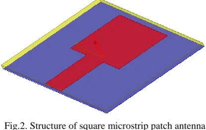
=1.5748mm), the work presented here is based on those simple geometries. The idea was to develop new configurations by modifying Defect Ground Structure (DGS) with notches. The performance of the antennas was analyses by HFSS software. The radiating element is selected to be a square patch Lp = Wp =14 mm and printed
on an inexpensive Duroid substrate. This material is light weight, and possesses a low dielectric constant (εr = 2.2).
It also has uniform electrical properties over a wide frequency range. In order to achieve a high radiation power without increasing the antenna weight and the dielectric loss, a 1.5748 mm thick substrate is selected from the available commercial Duroid substrate as shown in (Fig.2). A 50Ω microstrip line is used to feed the MSP antenna, and is printed on the same substrate. On the other side of the substrate, there is a ground plane chose to be (Lg × Wg =30×28 mm
2
) on the other side of substrate. The patch dimensions are selected to be Lp X Wp =14×14 mm2
on the top of the substrate and the width and length of feed lines are Lf × Wf = 4.8X12 mm2. The geometry and the
dimension of this antenna design are illustrated in (Fig. 2) and Table 1.
Fig.2. Structure of square microstrip patch antenna (MSPA).
Table 1: Dimensions of proposed square patch antenna.
Substrate material Duroid εr =2.2
Thickness of substrate (h) 1.5748 mm.
Length of ground plane ( Lg) 28 mm
Width of ground plane (Wg) 30 mm
Length and width of patch (Lp×Wp) 14 mm× 14 mm
Feed width and length (Wf×Lf) 4.8 mm×12 mm
Loss tangent (tan δ) 0.0009
The major formulas used for calculating antenna parameters are written as:-
1
2
2
0
r r
f
v
W
(1)L
f
v
L
reff r
2
2
0
Copyright © 2015 IJECCE, All right reserved 2
/ 1
12
1
2
1
2
1
W
h
r r
reff
(3)
0
.
8
264
.
0
258
.
0
3
.
0
412
.
0
h
W
h
W
h
L
r r
(4)
eff eff
f
c
L
0
2
(5)L
L
L
eff
2
(6)III.
R
ESULTSA
NDD
ISCUSSIONUsing HFSS simulator¸ the above antenna design is analysed (Fig. 3). The result of return loss characteristics are shown in (Fig. 4) without DGS. Return loss is a parameter which explains amount of power from feed point to radiating element is supplied effectively.
Fig.3. Defected ground structure (DGS) with double I slots of SMSP antenna.
Fig 4. Variation of S11 versus frequency of normal SMSPA.
The bandwidth percentage of the square patch antenna can be found by referring to resonant frequency or center frequency. The bandwidth percentage of the patch antenna can be calculated when its return loss becomes -10dB [11]. The resulting antenna bandwidth is summarized in (Table 2).
Table 2: Parameters of proposed SMSPA.
Parameters Value
fH 15.12 GHz
fL 13.62 GHz
fr 14.26 GHz
BW = fH- fL 1.5 GHz
BWr % = (BW/ fr)×100 10.5 GHz
The bandwidth percentage of square microstrip patch antenna without modifications is 10.5%. The 3D view for the gain and directivity of the antenna without DGS is also shown in (Fig. 5), the maximum gain is 6.9dB. The 2D radiation pattern of antenna is also shown in (Fig. 6) in which the fields are presented. In this radiation pattern both E and H planes are also presented.
Fig.5. 3D Polar plot of SMSP antenna: (a) Gain (b) Directivity without DGS at 14.26 GHz.
Fig.6. 2D Radiation pattern of SMSP antenna at 14.26 GHz.
Now, Return loss (S11), measurement take drastic change while antenna is designed with defected ground structure with reduced area and improve efficiency. It reduces the harmonics, area and enhances the bandwidth, feasibility, reliability, gain etc. Figure. 7 shows the return loss with DGS structure and Table 3 is the comparison table between simple microstrip patch antenna and microstrip patch antenna with DGS.
Copyright © 2015 IJECCE, All right reserved Table 3: SMSP antenna parameters with DGS of
Lg=20mm
Length of the ground Lg=20
mm
fL
GHz
fH
GHz
fr
GHz S11
dB
BWr
%
BW c %
First Band 12.5 15.5 13.53 -27 22 21 Second Band 15.6 18.3 17.32 -26 15.6 15 Third Band 20.22 28.85 23.87 -36 34 33
When the ground plane is reduced to12mm, two resonant frequencies (4.64 GHz and 12.07 GHz) for two bands of operation are obtained as shown in (Fig. 8) and (Tab. 4). Also the bandwidth of the antenna increases for each band.
Fig.8. Variation of SMSP antenna Return loss versus frequency operation with DGS of (Lg =12mm).
Length of the ground
Lg= 12 mm fL
GHz
fH
GHz
fr
GHz S11
dB
BWr
%
BWc
%
First Band 3.87 6.07 4.64 -17 47 44 Second
Band
10 14.5 12.07 -19.98 37 36
The reduction in the length of ground plane to 10.5mm results in a return loss values described in (Fig. 9) and in (Table 5). In this case the designed antenna resonates at 4.2 GHz with return loss of -26.5dB. It is noticed that the bandwidth with respect to resonance frequency was increases to 185% compared with 12% bandwidth of the antenna design without DGS.
Fig.9. Variation of SMSP antenna Return loss versus frequency operation with DGS of Lg=10.5 mm.
Table 5: SMSP antenna parameters with DGS of Lg= 10.5
mm Length of
the ground
Lg= 12 mm fL
GHz
fH
GHz
fr
GHz S11
dB
BWr
%
BWc
%
First Band 3.52 11.3 4.2, 11 -26.5 185 104
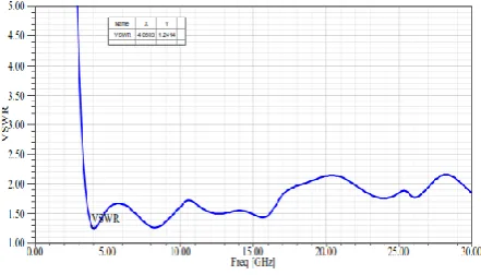
Figure 10, shows the VSWR values for designed antenna. The results show a satisfactory outcome that is less than 2.
Fig.10. VSWR versus frequency of the proposed antenna structure.
The radiation characteristics of antenna (SMSP antenna with DGS) are presented. The maximum gain at frequency of 4.06 GHz is 2.8966dB, this approaches omnidirectional radiation pattern, shown in (Fig. 11 a). An omnidirectional antenna is a class of antenna which radiates radio wave power uniformly in all directions in one plane, with the radiated power decreasing with elevation angle above or below the plane, dropping to zero on the antenna's axis. While, the directivity is 2.8982 dB as shown in (Fig. 11 b).
Fig.11. 3D Polar plot (a) Gain and, (b) Directivity of SMSP antenna with DGS.
IV.
C
ONCLUSIONIn this paper, microstrip fed rectangular patch antenna has been analyzed for return loss, VSWR and bandwidth for varying Lg. The use of DGS leads to broaden the bandwidth BW (with respect to center frequency) from 10.5% to 134% (3.42-17.45)GHz for rectangular patch, to 145%(2.3314.63) GHz. The size reduction is achieved of about 83.5% for rectangular microstrip antenna which could lead the opportunity to use in various microwave applications.
R
EFERENCES[1] D. Guha , M. Biswas and Y.M. Antar, “Microstrip Patch
Antenna with Defected Ground Structure for Cross Polarization
Suppression,” IEEE Antenna andWireless Propagation Letters,
Vol.4, 2005, pp. 455-458.
[2] C.A.Balanis , Antenna Theory, 3rd ed., Hoboken , NJ, John Wiley
& Sons, Inc.,ch.14, 2005, pp. 811-883.
[3] C. S. Kim , J. S. Park, D. Ahn and J. B. Lim, “An Improved 1-D
Periodic Defected Ground Structure for Microstrip Line,” IEEE Microwave and Wireless Components Letters, Vol.10, No.4, 2004, pp. 180-182.
[4] W.L. Strutzman and G.A.Thiele, Antenna Theory and Design,
Copyright © 2015 IJECCE, All right reserved
[5] E.O. Hammerstad, “Equations for Microstrip Circuit Design,”
Proc. Fifth European Microwave conf., 1975, pp. 268-272.
[6] F. Zavosh and James T. Aberle, “Improving the Performance of
Microstrip Patch Antennas,” IEEE Antenna and Propagation
Magazine, Vol.38, No.4, 1996, pp.712-721.
[7] S. N. Khan, J. Hu, J. Xiong and S. He, “Circular fractal
monopole antenna for low VSWR UWB applications,” Progress
in Electromagnetics Research Letters, Vol. 1, 2008, pp. 19-25. [8] J. S. Lim, Y. T. Lee, C. S. Kim, D. Ahn, and S. Nam, “A
vertically periodic defected ground structure and its application
in reducing the size of microwave circuits,” IEEE Microwave
Wireless Components. Lett., Vol. 12, no. 12, 2002, pp. 479–481.
[9] W. L. Chen and G. M. Wang, “Small size edge fed Sierpinski
Carpet Microstrip Patch Antennas,” Progress In
Electromagnetics Research, vol. 17, 2008, pp. 95-107.
[10] J. D. Krauss, Antennas for all applications, Third edition,
McGraw-Hill, 2001.
[11] J. Q. Howell, “Microstrip Antennas,” IEEE Trans. Antenna
Propagation, Vol. AP-23, 1975, pp. 90-93.