212
Copyright © 2011-15. Vandana Publications. All Rights Reserved.
Volume-5, Issue-2, April-2015
International Journal of Engineering and Management Research
Page Number: 212-216
Design of all Optical Encryption Decryption System Based on Cross Phase
Modulation in Semiconductor Optical Amplifier
Vipul Agarwal1, Vijayshri Chaurasia2
1,2
Electronics and Communication Department, INDIA
ABSTRACT
Optical encryption and decryption system is successfully demonstrated by using cross-gain modulation (XGM) in semiconductor optical amplifiers (SOAs). Transmission speed of 40 Gbps is successfully achieved.Our proposed scheme exploits cross phase modulation phenomenon in SOA. Our design is mainly based on SOA-Mach-Zehender interferometer structure , optical couplers, CW light & EDFA. Experimental evaluation using eye diagrams shows robustness of our proposed encryption decryption systems against eavesdropping.
Keywords— SOA, Cross Phase Modulation, Mach Zehender interferometer, EDFA, XOR, Bit error rate.
I.
INTRODUCTION
With continuous expansion of optical networks, the need for securing information flow through these networks is increasing day by day. To secure data while transmission, various encryption schemes have been proposed [1]-[3]. Most encryption technique however becomes difficult at bit rates exceeding 5 Gbps due to speed limitations of electronic optical interfaces. Hence a need exist for high speed, low latency optical encryption system which do not require opto electronic conversion. All optical XOR have attracted much attention as the building block of an all optical encryption system [4]-[6] because SOA possesses non linearity’s like four wave mixing, cross gain modulation & cross phase modulation. SOA also have wide gain spectrum, low power consumption, monolithic integration with other devices and low cost. Because of these advantages. SOA have been used extensively as non linear elements for optical processing. In the past many SOA based switching configuration have been demonstrated such as Tetra Hertz optical asymmetric demultiplexer (TOADs), ultrafast non linear interferometers(UNIs) and Mach Zehender
interferometer(MZIs). Monolithically integrated MZI switches offers most promising solution due to thin compact size, thermal stability & low power requirement. MZI interferometer can be constructed using two X coupler .The CW light beam is split equally in the two arms of the first input coupler. The light coming out of opposite port of coupler acquire π/2 phase shift due to longer arm length. These two beams are later recombined at the output of second X coupler .In SOA-MZI ,SOA is positioned in upper and lower arm of interferometer.SOA will introduce further phase shift in CW beam as intensity dependent signal depleted carrier density in SOA, which will modulate the Refractive index and thereby result in phase modulation of continuous wave signal. When CW wave is recombined, constructive or destructive interference will occur depending on the phase shifts introduced between the two paths of interferometer. The phase modulation experienced by CW wave is given by [7]
ΔΦ=2πno +α[log G- log Go] (i)
Where λ is the waveleng th of inp ut sign al travelling through SOA, L is length of active region of SOA, α is Line Width enhancement factor of SOA, no is
initial refractive index of SOA i.e in the absence of optical power ,G and Go are saturated gain and linear device gain
respectively.
213
Copyright © 2011-15. Vandana Publications. All Rights Reserved.
II.
PRINCIPLE
Our proposed encryption system is based on XPM effect [8 ].In this scheme CW light is provided as input to SOA along with intensity modulated data signal. Intensity modulated data signals influence the number of carriers in the SOA which in turn affects the gain and RI of SOA, which results in phase modulation of continuous wave signal. This phenomenon of phase modulation of CW beam through intensity modulated signals is known as XPM. Presence of CW beam as input to SOA can dramatically reduce carrier recovery time.[9].Carrier recovery time is an important parameter where high speed transmission is required.
III. IMPLEMENTATION
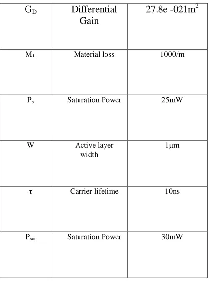
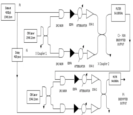
Optiwave Optisysytem 10 is used to simulate our experimental setup. The brief schematics of our proposed experimental setup is shown in Fig 1.The intensity modulated data signal is formed RZ format of wavelength 1548 nm with full width half maximum (FWHM) OF 1 MHz at 1mW .The data signal is denoted by Pi(Plaintext).The 212
SYMB OL
- 1 pseudorandom sequence generator is used to generate data at 40Gb/s. Security key , denoted by Ki is generated by delaying data signal by 400 ps. Both Pi and Ki is launched into Port A and Port C of the interferometer respectively. A CW light beam at at 1545 is launched into port B , comprising of 50:50 Y splitter in co propagating direction along with Pi and Ki signal. In the upper arm of an interferometer CW beam and Pi signal are together multiplexed in SOA using 2x1 mux . Similarly in lower arm Ki and CW beam are launched in SOA as shown in the figure. Combination of EDFA and attenuator is employed after WDM to control the power levels of signal to achieve maximum XPM efficiency. The parameter of SOA used in our Encryption & Decryption systems is shown in table 1.
PARAMETE RS
SOA PARAMETER
I Injection current
150mA
L Length of amplifier
500μm
Ŧ Optical confinement
factor
.3
G Differential Gain
D 27.8e -021m2
ML Material loss 1000/m
Ps Saturation Power 25mW
W Active layer
width
1μm
τ Carrier lifetime 10ns
Psat Saturation Power 30mW
Table 1. SOA Parameters
Encryption Process
Encryption process is achieved through all optical xor logic using semiconductor optical amplifier. An encrypted signal denoted by Ci can be explained in the form of equation:
Ci = Pi XOR Ki (ii)
The truth table for xor logic is shown in table 2
Pi Ki Ci
0 0 0
0 1 0
1 0 1
1 1 0
Table 2. Truth Table of XOR
214
Copyright © 2011-15. Vandana Publications. All Rights Reserved.
Fig 1. Proposed Encryption Decryption system
For Pi=0 & Ki=0, CW beam enters SOA-MZI & is split into two equal beams ,one passes through upper SOA and other through lower SOA .The beam that comes out of opposite port of coupler experiences a phase shift of π/2. In this manner CW beam travelling in upper and lower arm of interferometer have phase difference of π/2. Both SOAs in upper and lower arm of an interferometer remains in same condition as no data pulse has arrived. So no phase shift takes place while CW beam travels through SOAs and phase difference between upper and lower arm of an interferometer still remains π/2.These two beams after passing through SOA are combined at the output port of second X coupler where they suffer additional phase shift of π/2.So total phase difference induced between the two beam is π which means two CW beam interfere at the output of interferometer destructively, so no signal is obtained ie Ci=0.
In the case of Pi=1 and Ki=0, refractive index of upper SOA changes due to arrival of data pulse whereas lower SOA refractive index remains unchanged. As CW beam travel through upper and lower soa π phase shift is introduced between two beam due to different refractive index condition in two SOA.. Further π/2 phase shift in introduced due to x coupler. so total phase difference between two beam becomes 2π which means two CW beam interferes constructively so that we get Ci=1.For Pi=0 and Ki=1 two CW beams again interfere constructively so that Ci=1
In the case o f Ki=1 and Pi =1, π/2 phase difference is induced between two CW beam due to first X coupler. Refractive Index of both SOA changes due to arrival of a data pulse . So phase difference between two CW beam after travelling through upper and lower SOA remains π/2. Further π/2 phase shift is induced due to second X coupler ,so total phase difference between the two beam at the output of interferometer becomes π. So
CW beam interferes destructively which means Ci=0 Clearly our proposed circuit exactly works like a XOR
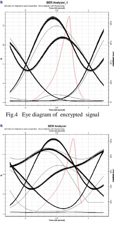
logic gate .The eye diagram of input signal before and after encryption is shown in fig 3 and fig 4 respectively
Decryption Process
Decryption of encrypted data can be achieved with XOR logic operation of Ci & Ki i.e
Pi=Ci XOR Ki
=(Pi Xor Ki)Xor Ki
The encrypted signal and delayed signal ki are applied to two inputs of optical coupler The parameters of SOA used in decryption setup are same as parameters of soa used in encryption setup.
To verify the operation of encryption decryption, a data sequence 1011 is used as pi and 1110 as ki ( pi sequence delayed by 2 bits).from fig 2 clearly shows that our logic circuit performs xor operation.
IV. SECURITY ANALYSIS AND
PERFORMANCE EVALUATION
This section analyzes the robustness of our proposed encryption decryption scheme. It is impossible for an eavesdropper to recover original signal due to large number of possible permutations of SOA parameters. Also
Fig 2 Experimental Waveform
215
Copyright © 2011-15. Vandana Publications. All Rights Reserved.
and 11.1mW output power for input signals of 1mW at 40Gb/s..These are improved results over results of ref [12], [13].The Q factor of decrypted signal is more than 7.5 at 40Gb/s as shown in fig 5, which is an improved results over ref[10] in terms of speed and Q factor of decrypted signal.
Tabulated comparison between various optical signal encryption schemes is given in table 3.
Author Name
Encryption Decryption technique
Bit rate
Q factor of decrypted
signal Jung at
al[10]
Optical encryption and decryption using
SOA without Use of CW beam
10G b/s
5.4
Abdalla h at.al[11]
Optical encryption and decryption using Optical delay lines
20G b/s
7.9
Agarwal at al
Optical encryption and decryption using
SOA with CW beam as input to
interferometer
40G b/s
7.8
Table 3. Comparision between different encryption schemes
Fig..3 Eye diagram of input signal
IV. CONCLUSION
The implementation of SOA-MZI based XOR logic in the presence of CW beam is simulated for secure data transmission in optical fiber networks. The results shows that decryption by an eavesdropper becomes impossible because large number of permutations of different parameters used in our encryption system. The results also show that there is no distortion in the decrypted signal .The demonstrated scheme offers compact
,low latency low power penalty approach at ultra high speed to secure confidential data in fiber optics networks.
Fig.4 Eye diagram of encrypted signal
Fig 5 Eye diagram of decrypted signal with correct Ki
REFERENCES
[1] C.A Barrios and M.Lipson, “Silicon photonic read only memory,” J.Lightwave Technol., vol. 24, no.7, pp. 2898-2905, jul.2006.
[2] G.C. Valley, “Photonic analog to digital converters,” Opt Exp., vol. 15, no.5, pp. 1955-1982, Mar.2007.
[3] F.F. Froehlich, C.H. Price, T.M. Turpin, and J.A. Cooke, “All optical encryption for links at 10 Gb/s and above,” in Proc.. IEEE Military Commun. Conf., vol. 4. Atlantic City. NJ. Oct. 2005, pp. 2158-2164
216
Copyright © 2011-15. Vandana Publications. All Rights Reserved.
semiconductor optical amplifiers without additional input beam,” IEEE Photon. Technol. Lett. Vol. 14, no. 10. Pp. 1436-1438. Oct. 2002.
[5] Q. Wang, G. Zhu ,H. Chen, J. Jaques, J. Leuthold,A. B.Piccirilli, and N.K. Dutta, ”Study of all- optical XOR using Mach-Zehnder interferometer and differential scheme, ”IEEE J.Quantum Electron., vol. 40, no. 6. pp. 703-710, Jun 2004.
[6] M.Zhang, L. Wang, and P.Ye, “ All optical XOR logic gates: Technologies and experiment demonstrations,” IEEE Commun. Mag., vol.43 ,no.5, pp. 519-524, May 2005.
[7] E. Lannone , R. Sabella, L. de Stefano , and F. Valeri, “ All optical wavelength conversion in optical multicarrier networks,” IEICE Trans. Commun., vol. 44, no 6, pp. 716-724, 1996.
[8] T.T Ng, “Characterization of XGM and XPM in a SOA-MZI using linear frequency resolved gating technique,” IEEE Lasers and Electro-Optics society, 2007, pp 656-657.
[9] Martin T. Hill, E. Tangdiongga, H. de Waardt, G.D. Khoe, and H.J.S. Dorren, “Carrier recovery time in semiconductor optical amplifiers that employ holding beams,”Optics Lett., vol. 27, No 18, pp 1625-1627 Sept 2002.
[10] Y.J. Jung , C.W. Son, S. Lee, S. Gill, H.S Kim,and N Park, “Demonstration of 10 Gb/s all encryption and decryption system utilizing SOA XOR logic gates,” J.Opt.Quantum Electron., vol 40, nos, 5-6, pp. 425-430 Apr.2008.
[11] W.Abdallah, M. Hamdi, N Boudriga, “An all optical configurable and secure OCDMA system implementation using loop based optical delay lines,” ICTON IEEE 2011.
[12] J.M. Martinez, F. Ramos and J. Marti, “10 Gb/s reconfigurable optical logic gate using a single hybrid-integrated SOA-MZI,”Int. J. Fiber Integr. Opt., vol27, no. 1,pp. 15-23, Jan 2008.
[13] S.Singh and S. Lovkesh, “Ultrahigh speed optical signal processing logic based on SOA-MZI,” IEEE J.sel. Topics Quantum Electron., vol 18, no 2, pp. 970-977, Mar.-Apr 2012.
[14] G.P. Agrawal, Fiber-Optic Communication system, 3rd ed. Singapore:Wiley. 2002. pp. 226-239.