Design and Simulation of Optical Power Splitter
By using SOI Material
NAGARAJU PENDAM* and C P VARDHANI1
*
Research Scholar, Department of Physics, Osmania University, Hyderabad, A.P., INDIA. 1Assistent Professor, Department of Physics,
Osmania University, Hyderabad, A.P., INDIA.
(Received on: April 16, 2013)
ABSTRACT
The present paper reports that the simple technology–compatible design of 1×2 optical power splitter is proposed. The device is based on symmetric Y-branch comprising of S-bend waveguide. Initially, a symmetric Y-junction based 1× 2 optical power splitter is designed, which can deliver the best result in simulated performance. Three dimensional Beam propagation Method is applied for this work, where S-bend waveguides are designed for optimal field matching in each Y-branch section of the optical splitter. Chosen wavelength in guiding media is 1550µm. Finally studied about insertion loss, attenuation, and splitting ratio. The SOI rib-waveguide dimensions (height, width) leading simultaneously to single mode propagation.
Keywords: Beam propagation method; Insertion loss; Optical
splitter; Y–junction Wave guide; Rib waveguides Silicon–on- Insulator.
INTRODUCTION
Optical Power splitter is one of the key passive components in subscribes networks of optical communications to split the power of the optical signal into two branches. Various research groups have designed, fabricated and demonstrated several techniques like Y-branch splitter,
propagation loss, high reliability and good fiber coupling efficiency due to its excellent inherent mechanical and thermal material properties.
In this paper, initially, a symmetric Y-junction-based 1×2 optical power splitter in silicon-on-insulator material is designed. The design is optimized for delivering the best possible simulated performance in terms of total insertion loss among the outputs. Finally, the simulation results of the proposed technology-compatible design of 1×2 optical splitter have been compared with that of the best designed splitter in terms of the same parameters showing the compromise in the design.
Design of a symmetric Y-junction optical splitter
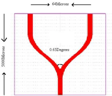
Fig.1 a schematic diagram of 1x2 Optical Power Splitter
The basic unit of the 1×2 Y-branch section optical splitter comprises of an initial straight waveguide, an S-bend waveguide. A pair of S-bend branching waveguides is considered in this case because of its
continuity in light propagation path with the S-bend waveguide, which results in a slight improvement in overall performance of the splitter. By symmetrically optical power splitter has been designed after considering silicon-on-insulator material parameters.
The BPM software tool has been used for the simulation work. The simulator is based on the unconditionally stable finite difference method algorithm of Crank and Nicolson. This method works with discrete values of the field, in the transverse direction (based on a numerical mesh) and the refractive index, along the direction of propagation (by steps of propagation). In this simulation, the number of points in mesh of 5000 and the propagation step of 1.55microns have been considered for the device dimension of 5000 µm (length) 64µm (width).
SIMULATION RESULTS AND DISCUSSION
The simulation has been done using BPM tool by considering the propagation of an optical signal of fundamental TE mode through the 1×2 optical splitter, where Figs 2, 3, 4 and 5 show the corresponding simulated results at 1550 nm, in terms of the variation of optical/electrical field and effective refractive index along the device length and across the device-width respectively. The simulated value of the average insertion loss of the splitter has been found to be 0.0813dB for TE-mode at this wavelength.
Fig.2 Simulation of the optical field along the Length
Fig.3 Simulation of field profile along its length
Fig.4 simulation of mode profile and refractive Index
Fig.5 simulation of prapagation along its length
TableI
Variation of Component width with Attenuation
Component Width (µm)
Transmitted Power(Watts)
IL (dB)
Attenuation (dB/m) 3 0.979 0.092 18.4 4 0.980 0.087 17.5 5 0.985 0.065 13.1
TableII
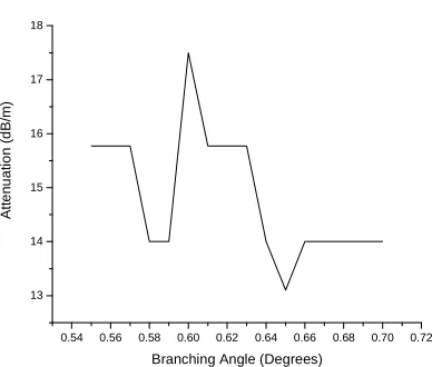
Variaton of Branching angle with Attenation
Branching angle(2θ) (Degrees)
Transmitted power
(Watts)
Power loss (dB)
Attenuation coefficient (dB)/m
0.55 0.982 0.078 15.77
0.56 0.982 0.078 15.77
0.57 0.982 0.078 15.77
0.58 0.984 0.070 14
0.59 0.984 0.070 14
0.60 0.980 0.087 17.5
0.61 0.982 0.078 15.77
0.62 0.982 0.078 15.77
0.63 0.982 0.078 15.77
0.64 0.984 0.070 14
0.65 0.985 0.065 13.1
0.66 0.984 0.070 14
0.67 0.984 0.070 14
0.68 0.984 0.070 14
0.69 0.984 0.070 14
0.70 0.984 0.070 14
Fig.6 Simulation of the index profile
(1)
Where in equation.1, r=h/H is the ratio of slab height to overall rib height, and W/H is the ratio of waveguide width to overall rib height (Fig. 6). Their analysis of the
waveguides was limited to shallow etched ribs (r> 0.5) and the waveguide dimensions were assumed to be larger than the operating wavelength. The analysis was based on the assumption that higher order vertical modes (i.e., modes other than the fundamental mode) confined under the rib, were coupled to the outer slab region during propagation, therefore yielding high propagation losses for the higher order modes. For a better understanding, we will also consider the etching depth (P) P=H (1-r) which directly gives the edge height of the rib waveguide1-6.
β = 2πneff/λ (2)
Where in equation.2, β is the propagation wave number with neff the effective index and λ the operating wavelength fixed at 1.55µm.
α = 10log10 (p1/p2) (3)
Where in equation.3, α is the Insertion loss of an optical splitter is usually measured in decibels. If an input power P1 (1 watts) results in an output power P2.
3.0 3.5 4.0 4.5 5.0
13 14 15 16 17 18 19
A
tt
e
n
u
a
ti
o
n
(d
B
/m
)
Component width ( microns)
0.54 0.56 0.58 0.60 0.62 0.64 0.66 0.68 0.70 0.72 13
14 15 16 17 18
A
tt
e
n
u
a
ti
o
n
(
d
B
/m
)
Branching Angle (Degrees)
Fig.8. Plot between Branching Angle with attenuation
CONCLUSION
The overall simulated performance of the proposed technology-compatible design of 1×2 optical splitter has been found to be comparable in terms of insertion loss (~ 0.01 dB higher) when compared to the results obtained from the best design; however, it should bring down the difference between the theoretical and experimental results with a better post-fabrication device performance. The splitting ratio of this
waveguide is almost symmetrical means 50/50. Width of waveguide is depend on splitter characteristics if the width is varied between 3-5µm and by fixing components (height, wavelength, refractive index difference) it is observed that the transmitted power increases, and also observed with the increase in width of the waveguide the transmitted power also increases. As well as it should vary with branching angle. It was found in fig 7, 8 and Table. II. The attenuation and Insertion loss depends on the width of the waveguide, Branching angle.
REFERENCES
1. R. A. Soref, IEEE J.Quantum Electron. 27 (1991).
2. U. Fischer, IEEE.8 (1996).
3. A. G. Rickman, Journal of Light wave Technology, 12( 1994).
4. A. G. Gickman, IEEE Proc-Optoelectro-nics,141(1994).
5. D.Dai, Appl.Opt, 43 (2004).